
Multilayer Graphene Grid and Nanowire Fabrication and Printing |
CONTENTS
29.2 Pattern Generation on HOPG
29.2.1 Preparation of a Micron-Scale Pattern
29.2.2 Preparation of a Nanoscale Pattern
29.3 Printing of the Patterned Graphene
29.3.1 Thermal Tape Method to Print onto Glass
29.3.2 Direct Printing of Graphene Nanowires onto PDMS
Molecular sensor development requires the fabrication of structures with nanometer precision. Recently, graphene or few-layer graphene (FLG) has been proposed as a material for making advanced electronic devices. The transport properties of graphene, a single-atom-thick layer of graphite (~0.35 nm) [1], are influenced by atomic-scale defects, and, more importantly from a sensor perspective, by adsorbates [2,3] and the local electronic environment. Highly oriented pyrolytic graphite (HOPG) is one of the best precursors for generating high-quality, crystalline graphene [1], which fortuitously is also an ideal substrate material for high-resolution atomic force microscope (AFM) studies [4]. Several approaches have been used to produce graphene for large-area electronics, including epitaxial growth [5, 6, 7 and 8], transfer-printing [9,10], electrostatic deposition [1,11], and solution-based deposition [12,13]. At the same time, efforts have been made to tailor graphene sheets into nanoscale features [9,14, 15, 16 and 17]. Keun et al. developed chemical vapor deposition (CVD) to grow a graphene layer on nickel films and transferred them to polydimethylsiloxane (PDMS) using an etching method [18,19]. However, the incompatibility between PDMS and the mechanical properties of graphene usually causes breaks during the fabrication process, especially during the etching step [20]. For large-scale production, CVD is a promising technique; however, the quality of the graphene layers (roughness) requires improvement. Novoselov et al. described a very simple sticky tape method [21]. First, press the adhesive tape onto a sample of graphite and pull. Then, repeatedly stick the carbon-covered tape against itself and peel away. Thereby, the first carbon flake breaks up further into thin, hundred-micron-wide fragments. Then, press this carbon-coated tape onto an Si surface and carefully remove the tape. Some single- or few-layer graphene will adhere to the Si substrate. However, one cannot mass-produce graphene with the sticky tape method. Liu et al. used a chemically modified silicon wafer to covalently attach graphene [22]. For graphene-based electronics, fabrication on chemically modified silicon will be difficult to control. To prepare a few hundred microns long graphene wires and to avoid the wet etching or chemical step, in this chapter, the authors demonstrate a different process for patterning HOPG, producing ordered features at the micron and ~100 nanometer scales. Two different methods are used to transfer the patterned graphene onto substrates for characterization, a thermal tape (T-tape) method to transfer onto glass and direct transfer onto a PDMS substrate, both performed without applying any electrostatic force [11].
29.2 PATTERN GENERATION ON HOPG
29.2.1 PREPARATION AF a MICRON-SCALE PATTERN
Ni transmission electron microscope (TEM) grids (SPI Inc., Mesh 2000 lines/inch, pitch 12.5 μm, bar width 5 μm, hole width 7.5 μm) were used as physical masks for the oxygen plasma lithography [21]. The TEM grids were placed on the HOPG (SPI Inc., ZYA grade) surface. Next, an O2 plasma was used to etch the graphite through the apertures in the TEM grid. A modified Harrick plasma etcher was used to produce the O2-based plasma employed for the 40 min periods with a pressure of 100 mTorr O2.
The scanning electron microscope (SEM) (JEOL 5310LV) imaging in the inset of Figure 29.1a (right upper corner) shows that the oxygen plasma lithography successfully replicates the TEM grid in the HOPG. The higher-resolution SEM image (Figure 29.1b) indicates that the grid pattern was uniformly etched. To determine the etching rate, an AFM topography analysis was performed for a 52 × 52 μm area (Figure 29.1c). The line profile analysis confirmed an average etch rate of 1.3 nm/min (Figure 29.1d). A Nano-R (Pacific Nanotechnology) AFM microscope was used to collect images of samples in noncontact mode using TM300-A (SensaProbes) AFM probes.
29.2.2 PREPARATION OF a NANOSCALE PATTERN
To produce patterns with finer features, we used phase-shift lithography [23], reducing the critical dimension in the product from 5 micron bars to ~100 nm wide (full width half maximum (FWHM)) lines. Freshly cleaved HOPG substrates were coated with 30% S1813 (MicroChem Corp.) photoresist (diluted with Thinner P from MicroChem Corp.), spun at 800 rpm for 10 s and 3000 rpm for 30 s, followed by a soft bake of 1 min at 116°C, exposed to UV for 30 s, and developed with 351 developer (Rohm and Haas) for 40 s. A PDMS mask was used for the phase mask [23]. After development, the features were etched into the resist patterned HOPG substrate using an O2-based plasma for 10 min at an etching rate of 1.3 nm/min (see above). Finally, the photoresist was removed by soaking/rinsing the HOPG substrate in acetone for 10 min.
Figure 29.2a presents the multilayer graphene (MLG) line pattern generated on the HOPG substrate after 10 min oxygen plasma etching. The topography line scan indicates Z = 10.2 nm, which is equivalent to ~29 graphene layers and ~100 nm width. The etching rate is consistent with the oxygen plasma etch rate indicated in Figure 29.1d. The 3D image of the high-resolution line pattern on HOPG is shown in Figure 29.2b. It indicates that the lines were continuous and were not interrupted by the graphene layers.
29.3 PRINTING OF THE PATTERNED GRAPHENE
29.3.1 THERMAL TAPE METHOD TO PRINT ONTO GLASS
T-tape from Nitto Denko Inc. was used to transfer the multilayer grid patterned graphene onto glass coverslips. First, T-tape was used to peel off thick MLG flakes, which contained the TEM grid pattern. Figure 29.3 shows a schematic illustration of this printing process. T-tape removes flakes that are thicker than the etched, patterned depth. Therefore, extra graphene layers were peeled off using scotch tape until the grid pattern was observable using optical microscopy. The T-tape with the MLG was placed side down on a plasma cleaned glass coverslip and thermal release of the MLG was accomplished by removing the tape after incubation at 120°C for 5 min.
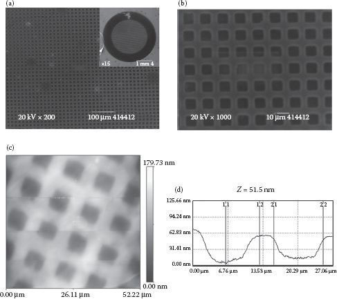
FIGURE 29.1 (a) SEM image of TEM grid pattern on HOPG produced using oxygen plasma lithography; inset (right upper corner) shows the replica of TEM grid on the HOPG substrate. (b) Higher-resolution SEM image of TEM grid pattern. ((a,b) Adapted from M. Rahman and M. Norton. Widefield optical and AFM analysis of few layer graphene nanowires functionalized with DNA, Extended abstract of a paper presented at Microscopy and Microanalysis, Nashville, Tennessee, August 7–11, 2011.) (c) AFM image of features produced. (d) Line profile analysis indicating Z = 51.5 nm/40 min etching rate. ((c,d) M. Rahman and M.L. Norton, 11th IEEE Conference on Nanotechnology (IEEE-NANO), Portland, OR, August 15–18, pp. 592–595. © (2011) IEEE. With permission.)
Figure 29.3 shows the schematic illustration of the process for transferring the patterned graphene onto glass slides using T-tape. During release, the T-tape also leaves some residue on the top of the patterned MLG. To remove this residue, we washed the transferred MLG with acetone for 5 min with sonication and finally rinsed with isopropanol and used N2 to blow the sample dry. Figure 29.4a shows a light microscopy (LM) image of the printed, patterned MLG on a glass coverslip. Darker regions mean that extra graphene layers, still remain. Although if we peel off more graphene layers using scotch tape, we could remove these extra graphene layers, this will also increase the loss of patterned graphene. AFM imaging was performed at the same printed region (Figure 29.4b). The arrow indicates a defect located in both the LM and AFM images. Line profile analysis (Figure 29.4c) confirmed that ~140 layers of graphene were printed onto the glass. The AFM result shows that some roughness remains and we believe that the automated process could not only decrease the roughness but also would provide more controllability of the number of graphene layers printed.
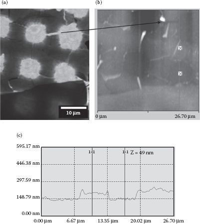
FIGURE 29.4 (a) Transmitted light microcopy image of MLG pattern on glass slide. (b) AFM image of the same region of the printed patterned MLG graphene on the glass slide. (c) Line profile indicating Z = 49 nm. (M. Rahman and M.L. Norton, 11th IEEE Conference on Nanotechnology (IEEE-NANO), Portland, OR, August 15–18, pp. 592–595. © (2011) IEEE. With permission.)
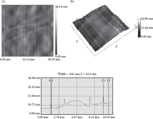
FIGURE 29.2 (a) AFM image of graphene ~100 nm FWHM line pattern on HOPG. (M. Rahman and M.L. Norton, 11th IEEE Conference on Nanotechnology (IEEE-NANO), Portland, OR, August 15–18, pp. 592–595. © (2011) IEEE. With permission.) (Adapted from M. Rahman and M. Norton. Widefield optical and AFM analysis of few layer graphene nanowires functionalized with DNA, Extended abstract of a paper presented at Microscopy and Microanalysis, Nashville, Tennessee, August 7–11, 2011.) (b) 3D image of high-resolution line pattern on HOPG.
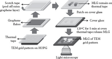
FIGURE 29.3 Schematic illustration of the process for printing the patterned graphene onto glass slides using thermal tape. (M. Rahman and M.L. Norton, 11th IEEE Conference on Nanotechnology (IEEE-NANO), Portland, OR, August 15–18, pp. 592–595. © (2011) IEEE. With permission.)
29.3.2 DIRECT PRINTING OF GRAPHENE NANOWIRES ONTO PDMS
Freshly prepared flat PDMS stamps (1 cm × 1 cm) were washed with toluene, then with ethanol, then oven dried for 2 h at 60°C, and finally plasma cleaned for 2 min before printing. The plasma cleaned PDMS stamps were then placed on the patterned HOPG surface. PDMS placement was started at one edge of the graphite sample and proceeded to the other edge with the application of gentle pressure using curved-style forceps. At the end of this process, the PDMS was securely attached to the HOPG. We then gently removed the printed FLG adhering to the PDMS from the HOPG surface, using an inverse peeling process. For optical microscopy analysis/imaging, the PDMS/FLG assembly was placed face down on a plasma cleaned glass coverslip.
The ~100 nm wide (FWHM) graphite nanowire was printed onto PDMS using soft lithography as illustrated in Figure 29.5. Figure 29.6a presents the LM image of the fourth print of FLG lines (or nanowires) onto PDMS. The graphene wire profile analysis result (Figure 29.6b) indicates that ~10 graphene layers were printed onto the PDMS. The profile was analyzed using ImageJ 1.43u NIH software and calibrated using the absorbance value provided by Nair et al. [26]. This result also indicates the transfer of patterned graphene nanowires along with additional graphene layers onto the PDMS substrate.
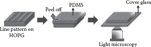
FIGURE 29.5 Schematic illustration of the method for printing graphene nanowires onto PDMS. (M. Rahman and M.L. Norton, 11th IEEE Conference on Nanotechnology (IEEE-NANO), Portland, OR, August 15–18, pp. 592–595. © (2011) IEEE. With permission.)
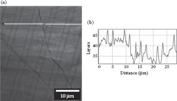
FIGURE 29.6 (a) Light microcopy image of FLG pattern on PDMS. (b) Plot profile of the printed graphene nanowires. (M. Rahman and M.L. Norton, 11th IEEE Conference on Nanotechnology (IEEE-NANO), Portland, OR, August 15–18, pp. 592–595. © (2011) IEEE. With permission.)
We have developed a method for printing graphene nanowires onto PDMS substrates without using any wet chemical processing. The potential for simplicity, speed, and reproducibility anticipated for lithographic patterning via contact printing on a transparent, biocompatible, and flexible surface makes this combination of methods and materials a strong candidate for nanofabrication of platforms supporting sensing nanoarchitectures. The process described in this report increases the potential of graphene as an improved substrate requiring simple chemical modification for the preparation of active sites for the potential localization of biomolecules such as DNA and for controlling the electrical conductivity of graphene wires.
The authors would like to express their sincere thanks to David Neff, Molecular and Biological Imaging Center, Marshall University, for the helpful discussion of ImageJ profile analysis. This work was supported financially by grants from NSF EPSCoR 0554328 and from the ARO G: W911NF-08-1-0109 and W911NF-11-1-0024.
1. A. N. Sidorov, M. M. Yazdanpanah, R. Jalilian, P. J. Ouseph, R. W. Cohn, and G. U. Sumanasekera, Electrostatic deposition of graphene, Nanotechnology, 18, 135301–135304, 2007.
2. F. Schedin, A. K. Geim, S. V. Morozov, E. W. Hill, P. Blake, M. I. Katsnelson, and K. S. Novoselov, Detection of individual gas molecules adsorbed on graphene, Nat Mater, 6, 652–655, 2007.
3. C. Berger, Z. Song, T. Li, X. Li, A. Y. Ogbazghi, R. Feng, Z. Dai et al., Ultrathin epitaxial graphite: 2D electron gas properties and a route toward graphene-based nanoelectronics, J Phys Chem B, 108, 9912–19916, 2004.
4. M. Rahman and M. L. Norton, Two-dimensional materials as substrates for the development of origamibased bionanosensors, IEEE Trans Nanotechnol, 9, 539–542, 2010.
5. C. Berger, Z. Song, X. Li, X. Wu, N. Brown, C. Naud, D. Mayou et al., Electronic confinement and coherence in patterned epitaxial graphene, Science, 312, 1191–1196, 26 2006.
6. S. Y. Zhou, G. H. Gweon, A. V. Fedorov, P. N. First, W. A. de Heer, D. H. Lee, F. Guinea, A. H. Castro Neto, and A. Lanzara, Substrate-induced bandgap opening in epitaxial graphene, Nat Mater, 6, 770–775, 2007.
7. J. Coraux, A. T. N’Diaye, C. Busse, and T. Michely, Structural coherency of graphene on Ir(111), Nano Lett, 8, 565–570, 2008.
8. L. Song, L. Ci, W. Gao, and P. M. Ajayan, Transfer printing of graphene using gold film, ACS Nano, 3, 1353–1356, 23 2009.
9. X. Liang, Z. Fu, and S. Y. Chou, Graphene transistors fabricated via transfer-printing in device activeareas on large wafer, Nano Lett, 7, 3840–3844, 2007.
10. J. H. Chen, M. Ishigami, C. Jang, D. R. Hines, M. S. Fuhrer, and E. D. Williams, printed graphene circuits, Adv Mater, 19, 3623–3627, 2007.
11. X. Liang, A. S. Chang, Y. Zhang, B. D. Harteneck, H. Choo, D. L. Olynick, and S. Cabrini, Electrostatic force assisted exfoliation of prepatterned few-layer graphenes into device sites, Nano Lett, 9, 467–472, 2009.
12. G. Eda, G. Fanchini, and M. Chhowalla, Large-area ultrathin films of reduced graphene oxide as a transparent and flexible electronic material, Nat Nanotechnol, 3, 270–274, 2008.
13. S. Stankovicha, D. A. Dikina, R. D. Pinera, K. A. Kohlhaasa, A. Kleinhammesc, Y. Jiac, Y. Wuc, S. T. Nguyenb, and R. S. Ruoff, Synthesis of graphene-based nanosheets via chemical reduction of exfoliated oxide, Carbon, 45, 1558–1565, 2007.
14. X. Wang, Y. Ouyang, X. Li, H. Wang, J. Guo, and H. Dai, Room-temperature all-semiconducting sub-10-nm graphene nanoribbon field-effect transistors, Phys Rev Lett, 100, 206803, 2008.
15. Y. Ouyang, Y. Yoon, J. K. Fodor, and J. Guo, Comparison of performance limits for carbon nanoribbon and carbon nanotube transistors, Appl Phys Lett, 89, 203107, 2006.
16. Y. Ouyang, Y. Yoon, and J. Guo, Scaling behaviors of graphene nanoribbon FETs: A three-dimensional quantum simulation study, IEEE Trans Electron Devices, 54, 2223–2231, 2007.
17. L. Tapaszto, G. Dobrik, P. Lambin, and L. P. Biro, Tailoring the atomic structure of graphene nanoribbons by scanning tunnelling microscope lithography, Nat Nanotechnol, 3, 397–401, 2008.
18. K. S. Kim, Y. Zhao, H. Jang, S. Y. Lee, J. M. Kim, J. H. Ahn, P. Kim, J. Y. Choi, and B. H. Hong, Large-scale pattern growth of graphene films for stretchable transparent electrodes, Nature, 457, 706–710, 5 2009.
19. S. Bae, H. Kim, Y. Lee, X. Xu, J. S. Park, Y. Zheng, J. Balakrishnan et al., Roll-to-roll production of 30-inch graphene films for transparent electrodes, Nat Nanotechnol, 5,574–578, 2010.
20. M. Rahman, H. A. Howells, and L. M. Norton, Patterning and transfer of graphene onto substrates for addressing biomolecules, in ACS 239th National Meeting, San Francisco, CA, 2010, p. COLL 20452.
21. K. S. Novoselov, A. K. Geim, S. V. Morozov, D. Jiang, Y. Zhang, S. V. Dubonos, I. V. Grigorieva, and A. A. Firsov, Electric field effect in atomically thin carbon films, Science, 306, 666–669, 2004.
22. L. H. Liu and M. Yan, Simple method for the covalent immobilization of graphene, Nano Lett, 9, 3375–3378, 2009.
23. M. Rahman and L. M. Norton, Hierarchical lithography for generating molecular testbeds, IEEE Sens J, 10, 498–502, 2010.
24. M. Rahman and M.L. Norton, 11th IEEE Conference on Nanotechnology (IEEE-NANO), 15–18 August 2011, pp. 592–595.
25. M. Rahman and M. Norton, Widefield optical and AFM analysis of few layer graphene nanowires functionalized with DNA, Extended abstract of a paper presented at Microscopy and Microanalysis, Nashville, Tennessee, August 7–11, 2011
26. R. R. Nair, P. Blake, A. N. Grigorenko, K. S. Novoselov, T. J. Booth, T. Stauber, N. M. R. Peres, and A. K. Geim, Fine structure constant defines visual transparency of graphene, Science, 320, 1308–1308, 2008.