
Integrating Low-Temperature Carbon Nanotubes as Vertical Interconnects in Si Technology |
CONTENTS
33.3.1 Surface Treatment of TiN
33.3.2 I–V Characterization of Top-Down Integrated CNT
33.3.3 Covering CNT for Bottom-Up
Since their discovery, many applications have been proposed for vertically aligned carbon nanotubes (CNT). Some potential areas for the use of CNT are supercapacitors [1], microelectromechanical systems (MEMS) [2], and displays [3]. For these applications, the unique high-aspect-ratio (HAR) features of CNT and their large surface area compared to their volume can be exploited. One promising application within microelectronics that has received a lot of attention is the use of aligned CNT as vertical interconnects [4].
CNT are attractive for interconnects as the currently used interconnect materials like Cu are approaching their physical limitations due to the continued downscaling in the semiconductor manufacturing process. In the roadmap for the semiconductor industry made by the International Technology Roadmap for Semiconductors (ITRS), it can be found that around 2015, for the highest-performance integrated circuits, the electrical current density in the interconnects surpasses the maximum current density of Cu, with no manufacturable known solutions available, as shown in Figure 33.1 [5]. CNT, on the other hand, have been demonstrated to be able to carry current densities up to 109 A/cm2 [6]. Besides that, CNT have been demonstrated to be able to transport heat very efficiently, with thermal conductivities up to 3500 W/mK being demonstrated at room temperature (in comparison, the thermal conductivity of Cu is about 343 W/mK) [7]. This could aid in decreasing the temperature of the interconnect stack, again aiding in improving reliability [8].
Besides the clear reliability advantage, several other issues exist within the interconnect technology. For local interconnects, which form the connections between logic blocks like adders, the interconnect sizes are being scaled with the same trend as the transistor size. Owing to this, the cross section of the interconnect has been pushed well into the nanometer regime. Due to grain boundary and surface scattering, the resistivity of Cu increases by 2–5 times the bulk value [9]. This effect becomes more severe when the interconnect size is further reduced. Owing to their onedimensional (1D) nature, CNT do not suffer from these scaling effects. However, this 1D nature does introduce a quantum resistance of 6.45 kΩ per single-walled nanotube (SWCNT), while the situation is slightly more complex for multiwalled nanotubes (MWCNT) [10]. This basically means that many parallel conducting tubes are required to achieve an electrical conductivity close to copper. Simulations have shown that dense, vertically aligned SWCNT bundles can indeed compete with Cu vias, while dense MWCNT bundles display a higher resistance [11,12]. Still, as via resistance is only a small part of the total interconnect resistance, a small increase can be acceptable if other properties like electrical reliability are superior to that of Cu.
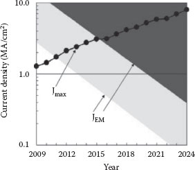
FIGURE 33.1 Progression of Jmax over the years according to the 2010 update of the ITRS roadmap. (From the International Technology Roadmap for Semiconductors, 2010, http://public.itrs.net/.)
For vertical interconnects (vias), a key requirement is thus selective growth of vertically aligned CNT directly on top of electrically conductive layers with high tube density. Without the direct growth on a conductive layer, difficult transfer techniques would be necessary to allow electrical contact to the CNT. For the best electrical performance, the CNT density should be high, as bundle resistance decreases if the number of tubes is increased as was mentioned before. Low-temperature deposition (preferably below 500°C, or 400°C for modern low-k dielectrics) is important to allow integration with already-fabricated devices (e.g., CMOS transistors). If growth temperature can be brought back down to 350°C, it will even allow growth on certain flexible substrates.
Two approaches can be defined to integrate interconnects: the traditional top-down approach and the bottom-up approach as presented by Li et al. [13]. Both methods are shown in Figure 33.2. In the top-down approach, a contact opening is etched using a plasma through the dielectric between the metal layers, followed by CNT growth inside the opening and subsequent metallization. In case CNT density is low and/or the CNT height is longer than the oxide thickness, planarization might be required. In case of the bottom-up approach, CNT bundles are first grown at the desired location, covered by a dielectric, planarized, and finally covered by the next metallization. The distinct advantage of the bottom-up method is that it allows the creation of HAR vias, without the need for the etching of, and metal deposition in, HAR openings. The bottom-up approach is also attractive for HAR MEMS [14].
Few publications exist that use mainstream silicon process technology to integrate low-temperature CNT growth, and combine this with electrical characterization of the as-grown CNT bundles. In this chapter, we demonstrate vertically aligned high-density growth of CNT on sputtered TiN layers at temperatures as low as 500°C. We found that specific processing steps used in silicon technology on an exposed TiN diffusion barrier can have a large impact on the CNT growth at low temperature. We will discuss the processing steps we found to be harmful to CNT growth, and a method to prevent damage. Using this, we demonstrate integrated top-down CNT via structures to measure the bundle resistance of the vertically aligned CNT grown at 500°C. Finally, we demonstrate that it is possible to use plasma-enhanced chemical vapor deposited (PECVD) silicon oxide and nitride to cover CNT for bottom-up integration.
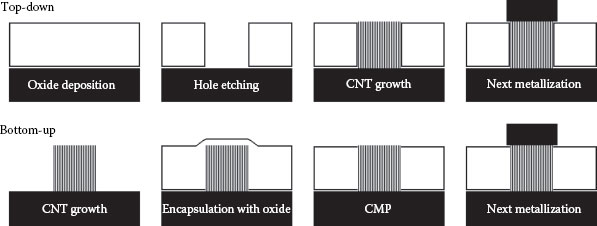
FIGURE 33.2 Graphical representation of top-down and bottom-up integration process.
In this section, we describe the process steps employed to create structures to electrically characterize the vertically grown CNT. Previously, we demonstrated that resist residues remaining after standard photolithography and wet etching of the catalyst during cleaning can negatively impact growth [15]. To prevent damage to the catalyst layer, we changed to a lift-off process using pure negative resist to pattern the Fe catalyst layer.
In case of a lift-off, a thin layer is deposited on top of a photoresist layer, and subsequently removed by dissolving the photoresist and “lifting off” the layer on top. This in contrast to general lithography, where a layer is removed by selective etching through a (photo-resist) mask. The minimum feature sizes obtained recently with this method are 0.8 μm holes and 0.5 μm lines, which is limited by our ASML PAS 5500/80 waferstepper. Another advantage of lift-off is that it allows the patterning of materials that are difficult to etch, like Pd, which we recently demonstrated to allow low-temperature, high-density vertically aligned growth [16].
CNTs are grown using a commercially available AIXTRON BlackMagic Pro 4″ chemical vapor deposition (CVD) reactor. We used 100 mm p-type Si wafers as substrates. For the measurement samples, we sputtered 500 nm of Ti and 50 nm of TiN on the Si wafers using an SPTS Sigma sputter coater. Then, 1.5 μm of tetraethyl orthosilicate (TEOS) is deposited using a Novellus Concept One PECVD reactor. After this, the wafer is coated with 1.5 μm AZ nLOF2020 negative resist, exposed, and developed. This is followed by dry etching of the oxide using an LAM Drytek 384T etcher with fluorine chemistry. The resist is not stripped but used to perform a lift-off, thus enabling automatic alignment. Before this, 5 nm of Fe is evaporated using a Solution CHA e-beam evaporator. Lift-off is performed with n-methyl-2-pyrrolidone (NMP) at 70°C. Normally, no ultrasonic treatment is required to completely remove the resist, making the method attractive for fabrication.
The catalyst layer is activated by annealing the sample inside the CNT reactor at 500°C with 700 sccm H2 flowing. During this step, the Fe layer is calcined and break up into a cluster of nanoparticles. From these nanoparticles, CNT can be grown using CVD. After 3 min, 50 sccm of C2H2 is added and CNT are grown for 5 min to reach the required height of 1.5 μm. During both steps, the pressure is regulated to 80 mbar. The CNT are covered by a second metallization of 100 nm of Ti and 3 μm of Al using sputtering. Finally, the Al and Ti layers are patterned using lithography and wet etching. In Figure 33.3, a scanning electron microscope (SEM) cross section of a CNT via can be found fabricated using this process with the different layer thicknesses indicated.
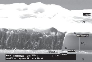
FIGURE 33.3 SEM cross section of CNT via fabrication using a described process with materials and thicknesses as indicated. Note that for this wafer 2 μm of TEOS was used.
To analyze the samples, we used an FEI/Philips XL50 SEM, Renishaw inVia Raman spectroscope with 633 nm laser, NT-MDT nTegra atomic force microscope (AFM), and an Agilent 4156C parameter analyzer in combination with a semiautomatic probe station. In case of Raman spectroscopy, three measurements are performed for each sample, which are averaged to increase accuracy.
In this section, we discuss the effect of different surface treatments on the TiN support layer and the resulting low- and high-temperature CNT growth on that layer. Afterward, using a sacrificial layer to protect the TiN, we employed the top-down approach to fabricate and subsequently electrically characterize the as-grown CNT bundles. Finally, we investigate the change in crystallinity of CNT bundles covered with PECVD oxide or nitride, which is required for bottom-up integration.
33.3.1 SURFACE TREATMENT OF TIN
We use TiN as a diffusion barrier for our electrical measurement structures, since it is not as sensitive to oxidation in air as Ti (and thus allows transfer of wafers between machines) and it is known to form a good electrical contact to CNT [17]. Besides that, TiN is a well-known diffusion barrier in semiconductor technology. It was found that certain common process steps used in semiconductor technology can induce microscopic changes in the TiN layer, preventing the low-temperature, self-aligned growth of CNT. We investigated the impact of chemical solutions and plasma treatment on the TiN and the subsequent low- and high-temperature CNT growth.
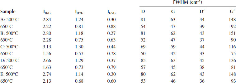
First, we investigate which treatments prevent low-temperature growth. For this, we created five different samples with the same TiN layer and exposed this layer to different conditions (see also Table 33.1): A: 10 min. 99.9% HNO3 (our standard metal clean); B: 1 min. 0.55% HF (used to etch SiO2 and Ti); C: 1 kW oxygen plasma (used for resist stripping); D: 100 W fluorine chemistry soft landing step used for oxide etching; E: pristine TiN. After this, we evaporated Fe and grew CNT at 500°C (low temperature) and 650°C (high temperature).
In Figure 33.4, the SEM images taken from the resulting CNT growth on the five different samples at low and high temperatures can be found. As can be directly observed, both plasma-treated samples display no self-aligned vertical growth at low temperature. The other three samples grow self-aligned CNT with a height of several microns. Interestingly, sample B displays the highest CNT (3.7 μm), followed by sample A (3.3 μm) and E (2.5 μm). We are unsure if this is caused by slight differences in the treated surface (HF might passivate the TiN surface) or due to small temperature differences in the reactor (as growth rate is highly temperature dependent). We approximate the tube density to be in the order of 1011 tubes/cm2 for all aligned samples, and using transmission electron microscopy, we determined the tube diameter to be in the range of 10–15 nm (not shown here).
TABLE 33.1
Overview of Surface Treatments Used on Different Samples
Sample |
Treatment |
A |
10 min HNO3 (99.9%) |
B |
1 min HF (0.55%) |
C |
5 min 1 kW oxygen plasma |
D |
1 min 100 W fluorine plasma |
E |
No treatment |
Source: S. Vollebregt et al., Integrating low temperature aligned carbon nanotubes as vertical interconnects in Si technology, 11th IEEE Conference on Nanotechnology, Portland, Oregon, August 15–19, pp. 985–990. © (2011) IEEE. With permission.
The high-temperature samples again display a difference between the samples A, B, E and C, D. Although self-aligned growth is now possible in all samples, the CNT height of sample C and D is approximately half of that of the other samples. Also, density and alignment suffer from plasma treatment. At high temperature, the length of samples A and B is found to be the same (31 μm), while E is slightly longer (35 μm), which is in contrast to the situation at low temperature.
Using Raman spectroscopy, we investigated if the treatment of the support layer influenced the crystal quality of the CNT growth. Raman spectroscopy is a nondestructive and fast method to investigate the crystallinity of CNT as several bands in the spectrum have been shown to be sensitive to defects [18]. Here, we investigated the D, D′, and G′ bands, and determined their intensity to the graphite reference G band. As is known from the literature, the ID/G and ID′/G ratios normally show a decline for increasing crystallinity, while IG′/G increases [18,19]. A decreasing band full width at half maximum (FWHM) is also associated with increasing crystallinity [18,20]. In Table 33.2, the intensity ratios and FWHM of the different Raman bands are listed.
Table 33.2 clearly shows that CNT grown at higher temperatures have higher crystallinity. The band ratios and widths of samples A, B, and E are close to each other, indicating that the chemical treatment of the TiN surface with either HNO3 or HF has no profound impact on CNT crystallinity. On the other hand, samples C and D display a different behavior. The ID/G ratio is significantly higher for the low-temperature C sample, and lower for the high-temperature C and D samples. This could indicate lower and higher crystallinity for the low- and high-temperature samples, respectively. On the other hand, the FWHM of the low-temperature growth on sample C suggests a higher crystallinity compared to samples A, B, D, and E. The changes in ID′/G and IG′/G are less profound. We can thus conclude that the plasma treatment appears to improve CNT crystallinity for the high-temperature samples, while for low temperature, the results are inconclusive.
To investigate the potential causes for the change in low- and high-temperature CNT growth on plasma-treated surfaces, we measured the sample surface after the treatment with AFM, which are shown in Figure 33.5. As can be seen, no significant difference exists between samples A and E (and B, which is not displayed here). Sample C, on the other hand, appears to have a more smooth surface (i.e., less sharp edges between the different TiN grains). The change in surface roughness is only minor and unlikely to be the cause for the change in growth. Sample D displays the largest change. It appears that the TiN layer was partly sputtered by the fluorine plasma, forming clusters of small particles. The surface morphology of sample D is changed extensively, which could account for the observed change in CNT growth on these samples.
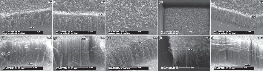
FIGURE 33.4 SEM images of CNT grown on differently treated TiN substrates at 500 and 650°C: (a)–(e) Samples A through E at 500°C; (f)–(j) Samples A through E at 650°C. See also Table 33.1 for an overview of treatment conditions for samples A through E. (S. Vollebregt et al., Integrating low temperature aligned carbon nanotubes as vertical interconnects in Si technology, 11th IEEE Conference on Nanotechnology, Portland, Oregon, August 15–19, pp. 985–990. © (2011) IEEE. With permission.)
TABLE 33.2
Raman Data Obtained from CNT Grown on Different Samples
Source: S. Vollebregt et al., Integrating low temperature aligned carbon nanotubes as vertical interconnects in Si technology, 11th IEEE Conference on Nanotechnology, Portland, Oregon, August 15–19, pp. 985–990. © (2011) IEEE. With permission.
To further examine the influence of the treatment on the TiN layer and subsequent CNT growth, we also performed AFM on samples on which the Fe catalyst was deposited and activated for CNT growth. The samples were placed in the CNT reactor after Fe evaporation, followed by 3 min of annealing at 500°C, while H2 was flowing. This is the default activation step for both low- and high-temperature CNT growth. After this, the samples were cooled down in a N2 environment. Figure 33.6 displays the AFM results. As can be seen, both samples A and E display small nanoparticles of similar size (the bigger bright spots on sample A are most likely particles deposited on the wafer during HNO3 treatment). The same holds for sample B (not shown here). On samples C and D, however, besides the small nanoparticles, a significant amount of larger nanoparticles can be found. This will result in CNT growth with large diameter distribution and, most likely, lower density. This can explain the absence of self-alignment at low growth temperatures for samples C and D. It can also explain the higher crystal quality observed by Raman spectroscopy on those samples. As found by Antunes et al. [20], CNT grown from larger nanoparticles at the same temperature show a lower ID/G, ID′/G, and FWHM, and a higher IG′/G. This, however, does not account for the large ID/G ratio observed for the low-temperature C sample. Sample D has low-temperature Raman data that match closer with that obtained from sample E. Indeed, the nanoparticle distribution of sample D is, with respect to sample C, more similar to that of sample E.
Increased surface roughness of sample D is most likely the cause of the observed broader particle deposition. For sample C, we believe that the oxidation of the TiN surface due to the oxygen plasma (in case of our Ti/TiN stack, sheet resistance increases from 1.158 Ω/sq to 1.165 Ω/sq) alters the surface properties in such a way that activation of the catalyst layer becomes more difficult.
33.3.2 I–V CHARACTERIZATION OF TOP-DOWN INTEGRATED CNT
We created four-point probe vertical interconnect measurement structures using a top-down approach as described in the experimental section and shown in the inset of Figure 33.8. To protect the TiN layer from damage during plasma etching, we sputtered an additional 100 nm of Ti on top of this layer before TEOS deposition. During the contact opening etch, we stop on this layer without completely removing it (the etch rate of Ti is low in our fluorine etcher). Before Fe evaporation, we remove the sacrificial Ti layer by a short 60 s etch in 0.55% HF. Using this method, we are able to grow perfectly aligned high-density bundles of CNT within the contact openings at 500°C; see also Figure 33.7a. As the CNT height was controlled to be the same as the depth of the opening, no planarization is required for the second metallization. As can be seen in Figure 33.7b, good contact is achieved, although some irregularities exist between the bulk metal and the metal on the CNT due to the small spacing between the oxide opening and the CNT bundle.
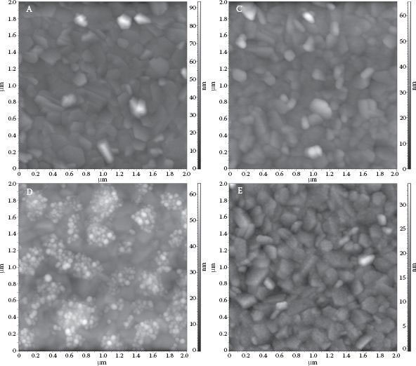
FIGURE 33.5 AFM images taken from samples A, C, D, and E displaying the effect of the surface treatments on the TiN surface. (S. Vollebregt et al., Integrating low temperature aligned carbon nanotubes as vertical interconnects in Si technology, 11th IEEE Conference on Nanotechnology, Portland, Oregon, August 15–19, pp. 985–990. © (2011) IEEE. With permission.)
We measured the resistivity of the square and round CNT bundles with different diameters. The resulting I–V characteristics of the square structures can be found in Figure 33.8. As can be seen, all structures display good linearity, indicating good metal–CNT contact without a significant Schottky barrier.
The resistivities of the structures can be found in Figure 33.9. For comparison, we also added values of several publications found in the literature [21, 23 and 24]. As can be seen, smaller structures suffer from an increase in resistivity, probably caused by a combination of a not-yet optimized lithographic process that slightly undersizes the smaller structures. A good match can be found between the square and round structures, indicating that for this size, there is no preferential morphology for creating CNT vertical interconnect bundles, as expected. We also measured the resistivity of structures consisting of four smaller bundles spaced by 3 μm with a total area of a larger bundle (e.g., 4 × 4 μm to get the same area as a single 8 μm bundle). As can be seen from Figure 33.9, the resistivity of a single large bundle is always lower than that of several smaller bundles.
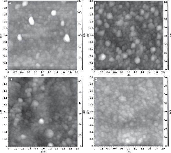
FIGURE 33.6 AFM images taken from samples A, C, D, and E displaying the catalyst nanoparticles after activation. (S. Vollebregt et al., Integrating low temperature aligned carbon nanotubes as vertical interconnects in Si technology, 11th IEEE Conference on Nanotechnology, Portland, Oregon, August 15–19, pp. 985–990. © (2011) IEEE. With permission.)
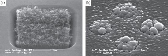
FIGURE 33.7 SEM images taken from CNT growth in contact openings (a) before and (b) after metallization. (S. Vollebregt et al., Integrating low temperature aligned carbon nanotubes as vertical interconnects in Si technology, 11th IEEE Conference on Nanotechnology, Portland, Oregon, August 15–19, pp. 985–990. © (2011) IEEE. With permission.)
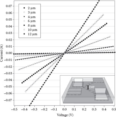
FIGURE 33.8 I–V measurements of structures with different bundle sizes. Inset: Four-point probe measurement structure.
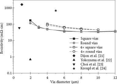
FIGURE 33.9 Extracted resistivity of structures with different diameter and morphology compared to other values found in the literature. (S. Vollebregt et al., Integrating low temperature aligned carbon nanotubes as vertical interconnects in Si technology, 11th IEEE Conference on Nanotechnology, Portland, Oregon, August 15–19, pp. 985–990. © (2011) IEEE. With permission.)
Compared to the other values found in the literature, our average resistivity of 35 mΩ-cm is between the lowest and highest found. It must be noted that the value from Yokoyama et al. [22] is achieved with structures fabricated with very specific equipment after a long optimization process, while our reported values are not yet optimized. Our growth temperature (500°C) is relatively low compared to the temperatures used by Dijon et al. (590°C, [21]), Choi et al. (600°C, [23]), and Kreupl et al. (700°C, [24]). We believe our resistivity can still be reduced by at least one order of magnitude by further optimizing our process.
As the CNT all have diameters between 10 and 15 nm, the grown CNT are multiwalled, which implies that they are all (semi)metallic [25]. This is confirmed by the Raman spectra (not shown here), which do not show any radial breathing modes, the fingerprints of SWCNT [26]. To accurately determine the average tube resistivity, we require the contact resistance, which is nonneglectable for CNT. In a recent publication, we investigated the CNT resistance versus length to determine the contact resistance, and found that this resistance is low compared to the CNT bundle resistance [27]. We attribute this to embedding of the CNT tips by the sputtered Ti layer used for the second metallization.
33.3.3 COVERING CNT FOR BOTTOM-UP
To allow low-temperature bottom-up integration, CNT have to be covered by a low-temperature dielectric, in contrast to the high-temperature LPCVD TEOS used by Li et al. [13]. For low-temperature dielectric deposition, PECVD is the preferred method in the semiconductor industry. However, it is likely that the plasma might damage the grown CNT by ion bombardment or oxidation. To investigate this, we grew freestanding bundles of CNT with a height of approximately 5 μm on TiN substrates (Figure 33.10a) and covered them with PECVD TEOS, silicon oxide, and nitride at temperatures of 400, and 350°C for the TEOS deposition.
Figure 33.10b shows an SEM image taken of an array of 5 × 5 2-μm-wide CNT bundles covered by 1 μm TEOS (deposited using TEOS and O2). As can be seen, good step coverage is achieved, although deposition on the sidewalls of the CNT is lower compared to the total thickness of the TEOS layer (approximately 600 nm). In Figure 33.10c, the same array is completely covered by 5 μm of PECVD oxide (deposited from SiH4 and N2O). Planarization will be necessary to remove the excess oxide. Finally, Figure 33.10d shows the array covered by 200 nm silicon nitride (from SiH4 and NH3). As can be seen, for unknown reasons, the deposition is significantly less smooth compared to the oxide depositions.
Using Raman spectroscopy, we investigated the CNT crystallinity before and after PECVD dielectric deposition of 1 μm of TEOS or oxide and 200 nm nitride. As can be seen in Figure 33.11, only minor changes to the crystallinity can be observed. The TEOS deposition appears to induce the least amount of damage, with only the width of the D band (around 1330 cm−1) increasing slightly. Oxide deposition from silane and nitrous oxide, on the other hand, display an increase of the D band, indicating less crystallinity. The width of the D band is similar to that of the D band after TEOS deposition. Finally, nitride deposition has a D band intensity in between that of CNT covered by TEOS and oxide. Again, the width of the D band is similar to that of the TEOS-covered CNT. In the second-order band region, changes are even smaller (not shown here). We can thus conclude that PECVD deposition does not induce a significant amount of defects in the CNT bundles, opening up the possibility to use this method for low-temperature, bottom-up integration. TEOS deposition appears to be an especially attractive candidate. In a recent publication, we measured CNT structures fabricated using this bottom-up approach and demonstrated that the resistivity is in the same order of magnitude as the results displayed here [28].
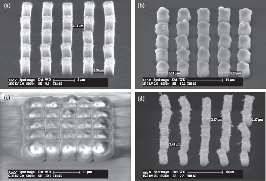
FIGURE 33.10 SEM images of (a) freestanding bundles grown on TiN, (b) bundles covered by 1 μm TEOS, (c) bundles covered by 5 μm SiO2, and (d) bundles covered by 200 nm Si3N4. (S. Vollebregt et al., Integrating low temperature aligned carbon nanotubes as vertical interconnects in Si technology, 11th IEEE Conference on Nanotechnology, Portland, Oregon, August 15–19, pp. 985–990. © (2011) IEEE. With permission.)
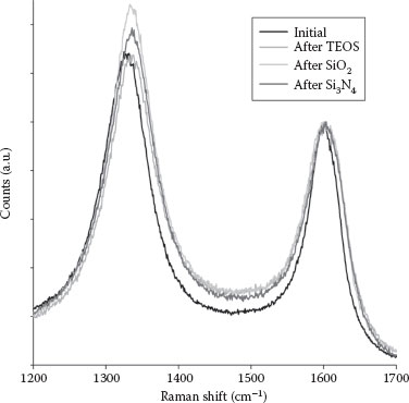
FIGURE 33.11 Raman spectra of CNT before and after covering with PECVD dielectrics. The intensity is normalized to the G-band at 1580 cm−1. (S. Vollebregt et al., Integrating low temperature aligned carbon nanotubes as vertical interconnects in Si technology, 11th IEEE Conference on Nanotechnology, Portland, Oregon, August 15–19, pp. 985–990. © (2011) IEEE. With permission.)
We demonstrated the high-density, low-temperature, vertically aligned growth of CNT on conductive TiN layers deposited on Si substrates. It was found that plasma bombardment can damage the TiN diffusion barrier, while wet chemical cleaning has no apparent impact. From the AFM measurements, it was observed that the plasma-treated samples display a broader distribution of catalyst nanoparticles after activation. This can account for the lack of self-aligned vertical growth at low temperature. With a sacrificial Ti layer, damage can be prevented.
Using this approach, we successfully created CNT via measurement structures, displaying a relative low resistivity of 35 mΩ-cm and linear I–V characteristics, indicating good ohmic contact between the metal contacts and CNT. Finally, we demonstrate that it is possible to use PECVD dielectrics to cover CNT without inducing significant damage to the CNT, which can be used for bottom-up processes. TEOS appears to be an especially attractive candidate, introducing hardly any change in CNT crystallinity.
Both methods are simple and effective to fully integrate CNT as vertical interconnects in silicon process technology. Although the resistivity is still high compared to that of Cu, further process and CNT growth optimization should be able to decrease its value.
The authors would like to thank M. R. Tajari Mofrad for assistance during the electrical measurements and the Dimes Technology Centre staff for all fabrication support. A part of the work has been performed in the project JEMSiP_3D, which is funded by the Public Authorities in France, Germany, Hungary, the Netherlands, Norway, and Sweden, as well as by the ENIAC Joint Undertaking.
1. D. N. Futaba, K. Hata, T. Yamada, T. Hiraoka, Y. Hayamizu, Y. Kakudate, O. Tanaike, H. Hatori, M. Yumura, and S. Iijima, Shape-engineerable and highly densely packed single-walled carbon nanotubes and their application as super-capacitor electrodes, Nature Materials, 5, 987–994, 2006.
2. Y. Hayamizu, T. Yamada, K. Mizuno, R. C. Davis, D. N. Futaba, M. Yumura, and K. Hata, Integrated three-dimensional microelectromechanical devices from processable carbon nanotube wafers, Nature Nanotechnology, 3, 289–294, 2008.
3. S. Fan, M. G. Chapline, N. R. Franklin, T. W. Tombler, A. M. Cassell, and H. Dai, Self-oriented regular arrays of carbon nanotubes and their field emission properties, Science, 283, 512–514, 1999.
4. J. Robertson, Growth of nanotubes for electronics, Materials Today, 10(1–2), 36–43, 2007.
5. International Technology Roadmap for Semiconductors, 2010, http://public.itrs.net/.
6. B. Q. Wei, R. Vajtai, and P. M. Ajayan, Reliability and current carrying capacity of carbon nanotubes, Applied Physics Letters, 79(8), 1172–1174, 2001.
7. E. Pop, D. Mann, Q. Wang, K. Goodson, and H. Dai, Thermal conductance of an individual single-wall carbon nanotube above room temperature, Nano Letters, 6(1), 96–100, 2006.
8. N. Srivastava, H. Li, F. Kreupl, and K. Banerjee, On the applicability of single-walled carbon nanotubes as VLSI interconnects, IEEE Transactions on Nanotechnology, 8(4), 542–559, 2009.
9. S. M. Rossnagel, R. Wisnieff, D. Edelstein, and T. S. Kuan, Interconnect issues post 45 nm, in International Electron Devices Meeting (IEDM), 2005, pp. 89–91.
10. A. Naeemi and J. D. Meindl, Carbon Nanotube Electronics, ser. Series on Integrated Circuits and Systems. Springer US, 2009, ch. Performance Modeling for Carbon Nanotube Interconnects, pp. 163–190.
11. H. Li, N. Srivastava, J.-F. Mao, W.-Y. Yin, and K. Banerjee, Carbon nanotube vias: A reality check, in International Electron Devices Meeting (IEDM), 2007, pp. 207–210.
12. H. Li, N. Srivastava, J.-F. Mao, W.-Y. Yin, and K. Banerjee, Carbon nanotube vias: Does ballistic electronphonon transport imply improved performance and reliability, IEEE Transactions on Nanotechnology, 58(8), 2689–2701, 2011.
13. J. Li, Q. Ye, A. Cassell, H. T. Ng, R. Stevens, J. Han, and M. Meyyappan, Bottom-up approach for carbon nanotube interconnects, Applied Physics Letters, 82(15), 2491–2493, 2003.
14. D. N. Hutchison, N. B. Morrill, Q. Aten, B. W. Turner, B. D. Jensen, L. L. Howell, R. R. Vanfleet, and R. C. Davis, Carbon nanotubes as a framework for high-aspect-ratio MEMS fabrication, Journal Of Microelectromechanical Systems, 19(1), 75–82, 2010.
15. S. Vollebregt, R. Ishihara, J. Derakhshandeh, W. H. A. Wien, J. van der Cingel, and C. I. M. Beenakker, Patterned growth of carbon nanotubes for vertical interconnect in 3D integrated circuits, in Proceedings of The Annual Workshop on Semiconductor Advances for Future Electronics and Sensors, 2010, pp. 184–187.
16. S. Vollebregt, J. Derakhshandeh, R. Ishihara, M. Y. Wu, and C. I. M. Beenakker, Growth of high-density self-aligned carbon nanotubes and nanofibers using palladium catalyst, Journal of Electronic Materials, 39(4), 371–375, 2010.
17. S. Sato, M. Nihei, A. Mimura, A. Kawabata, D. Kondo, H. Shioya, T. Iwai, M. Mishima, M. Ohfuti, and Y. Awano, Novel approach to fabricating carbon nanotube via interconnects using size-controlled catalyst nanoparticles, in IEEE International Interconnect Technology Conference, 2006, 230–232.
18. S. Vollebregt, R. Ishihara, F. D. Tichelaar, Y. Hou, and C. I. M. Beenakker, Influence of the growth temperature on the first and second-order raman band ratios and widths of carbon nanotubes and fibers, Carbon, 50, 3542–3554, 2012.
19. Y. -J. Lee, The second order raman spectroscopy in carbon crystallinity, Journal of Nuclear Materials, 325, 174–179, 2004.
20. E. F. Antunes, A. O. Lobo, E. J. Corat, and V. J. Trava-Airoldi, Influence of diameter in the Raman spectra of aligned multi-walled carbon nanotubes, Carbon, 45, 913–921, 2007.
21. J. Dijon, H. Okuno, M. Fayolle, T. Vo, J. Pontcharra, D. Acquaviva, D. Bouvet et al., Ultra-high density carbon nanotubes on Al-Cu for advanced vias, in International Electron Devices Meeting (IEDM), 2010, p. 33.4.1.
22. D. Yokoyama, T. Iwasaki, K. Ishimaru, S. Sato, T. Hyakushima, M. Nihei, Y. Awano, and H. Kawarada, Electrical properties of carbon nanotubes grown at a low temperature for use as interconnects, Japanese Journal of Applied Physics, 47(4), 1985–1990, 2008.
23. Y. -M. Choi, S. Lee, H. S. Yoon, M.-S. Lee, H. Kim, I. Han, Y. Son, I.-S. Yeo, U.-I. Chung, and J.-T. Moon, Integration and electrical properties of carbon nanotube array for interconnect applications, in Nanotechnology, 2006. IEEE-NANO 2006. Sixth IEEE Conference on, 2006, 262–265.
24. F. Kreupl, A. P. Graham, G. S. Duesberg, W. Steinhögl, M. Liebau, E. Unger, and W. Hönlein, Carbon nanotubes in interconnect applications, Microelectronic Engineering, 64, 399–408, 2002.
25. A. Naeemi and J. D. Meindl, Compact physical models for multiwall carbon-nanotube interconnects, IEEE Electron Device Letters, 27(5), 338–340, 2006.
26. M. S. Dresselhaus, G. Dresselhaus, R. Saito, and A. Jorio, Raman spectroscopy of carbon nanotubes, Physics Reports, 409, 47–99, 2005.
27. S. Vollebregt, R. Ishihara, F. D. Tichelaar, J. van der Cingel, and K. Beenakker, Electrical characterization of carbon nanotube vertical interconnects with different lengths and widths, in IEEE International Interconnect Technology Conference, 2012.
28. S. Vollebregt, R. Ishihara, J. van der Cingel, and K. Beenakker, Low-temperature bottom-up integration of carbon nanotubes for vertical interconnects in monolithic 3D integrated circuits, in Proceedings of the 3rd IEEE International 3D System Integration Conference, 2012, 1–4.
29. S. Vollebregt, R. Ishihara, J. Derakhshandeh, J. Cingel van der, H. Schellevis, and C. I. M. Beenakker, Integrating low temperature aligned carbon nanotubes as vertical interconnects in Si technology, 11th IEEE Conference on Nanotechnology, Portland, Oregon, August 15–19, 2011, pp. 985–990.