
Electrical Control of Synthesis Conditions for Locally Grown CNTs on a Polysilicon Microstructure |
CONTENTS
37.3 Characterization of CNT Growth Structure
37.3.1 Calculation and Simulation
37.3.2 Experimental Characterization
37.5 Outlook and Potential Industrial Implementation
The integration of carbon nanotubes (CNTs) with micro-electromechanical systems (MEMS) or nano-electromechanical systems (NEMS) has attracted increasing interest over the last decade [1, 2, 3, 4, 5, 6 and 7]. Recent semiconductor advancements further demonstrate the feasibility of using CNTs to construct nano-devices [3, 2, 3, 4, 5, 6 and 7]. The possibility of combining CNTs with on-chip integrated circuits (ICs) and MEMS enables many applications of CNTs in devices, including physical, chemical, and biological sensors, as well as nanotube-based transistors. Combining the three technologies on a single platform will allow for true integration of micro–nano systems. CNTs with their huge surface-to-volume ratio give ultra-sensitive sensors, ICs/CMOS provide signal processing capability, and MEMS give actuation opportunities as well as further sensor options.
To combine CNTs with MEMS and IC technologies, a desirable approach is to construct the on-chip microelectronics first using readily available foundry services and synthesize or assemble CNTs selectively at desired locations afterward. CNTs are normally synthesized in bulk volumes by arc discharge, laser ablation, or chemical vapor deposition at high temperatures, above 700°C, which is far higher than the acceptable post-processing temperatures for circuits from standard foundry services. Processed CMOS/MEMS devices should normally not be exposed to temperatures above 300–400°C, depending on the duration of high-temperature exposure. In situ manufacturing of CNTs on an IC (CMOS) device is therefore not compatible with these high-temperature CNT manufacturing techniques. Alternatively, CNTs can be synthesized separately and deposited on the microsystem, but it is difficult to control the deposition locations of CNTs, and to obtain a reliable and low-cost assembly process. A number of ways to integrate CNTs in microsystems and ICs have been proposed and demonstrated:
• Manual transfer of CNTs by micro-manipulators, and welding the terminals of the CNTs to MEMS structures using electron or ion-beam-induced metal deposition in an SEM and/or FIB [8]. Whereas this has indeed been successfully demonstrated on a research laboratory scale, the technique relies on a serial process occupying high-cost equipment, and is therefore not scalable to a low-cost industrial manufacturing process.
• Dielectrophoresis allows the alignment of CNTs between the given electrodes [9]. However, this process will also rely on a separate process for electrical connection of the CNTs to the microstructure, such as the above-mentioned electron-beam or ion-beam metal deposition. Similar to the above, this implies that the process is not compatible with manufacturing in an industrial setting.
• Processing from a solution of CNTs, low-temperature and low-cost deposition of CNTs is possible [10]. This technique will, however, result in random CNT networks not utilizing the properties of single CNTs as the CNT-to-CNT interconnects are likely to dominate the performance. Furthermore, additional patterning is needed to locate the CNT network in the desired area, which is normally performed through a photolithography process.
• CNTs grown on a separate wafer can be transferred to the active wafer [11]. The cited process requires a number of process steps, including Au evaporation on top of the CNTs, thermal release tape transfer of Au + CNT, and Au etching. Also, CNT patterning as well as metal connection deposition is needed in this case.
Heading for a low-cost CMOS-compatible process of CNT–microsystem integration, a local synthesis technique that uses local Joule heating has been studied and developed by Christensen et al. [1,2] on SOI structures, thus demonstrating the direct integration of CNTs on a Si microsystem at room temperature. Similar approaches have been addressed by other groups, using SOI [12], or metal [13,14] growth structures.
Selected properties of the methods described above are summarized in Table 37.1, focusing on the relevance for low-cost, industrially relevant processes for CNT–microsystem integration.
This study presents the local synthesis and direct integration of CNTs on polysilicon microstructures fabricated from a commercial process (PolyMUMPS), thus investigating the applicability for the CNT direct integration on a realistic device platform. Furthermore, we present a method to automatically control the entire growth process, in particular the important local synthesis temperature. This control method uses only the measurement of electrical resistance of the structure; therefore, it is more cost-effective and less time consuming than other methods that require additional optical equipment to determine optimum growth conditions. Importantly, it is scalable to wafer-level processing and well adapted to be implemented in an industrial setting.
To demonstrate the concept, we use a microstructure, shown in Figure 37.1, consisting of two suspended polysilicon microbridges, 5 μm wide and 160 μm long. The two microbridges are separated by 15 μm, and they are suspended 3.5 μm above the substrate. The suspended bridge structure is obtained through the etching of a 3.5 μm sacrificial layer in the PolyMUMPS process. A dual layer of 3 nm Fe and 2 nm Ni is evaporated to serve as the catalyst. Such thin layers do not result in a short-circuit over the microstructure. The catalyst film is not patterned, since the areas for CNT growth will be selected by the localized resistive heating. The synthesis is accomplished using resistive heating on the growth structure while a local electric field is established between the two bridges to guide the growth direction of CNTs [1,2]. The electrical arrangement is also illustrated in the figure. The synthesis is conducted in a room temperature chamber with a pressure of 0.4 bar, acetylene (C2H2) gas flow of 30 ccm (cubic centimeter per minute) after the growth structure is heated to the desired temperature (850–950°C). When CNTs grown connect the two microbridges, individual connections are detected electrically, with the current between the two microbridges increasing in steps every time a new CNT connection is made.
TABLE 37.1
Comparison of Different Processes for CNT–Microsystem Integration
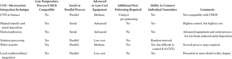
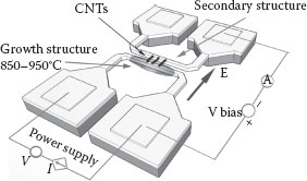
FIGURE 37.1 Polysilicon microstructures and electrical arrangement. The growth structure is heated by Joule heating. CNTs grow from the growth structure, and connect to the secondary structure under the assistance of an electric field.
To get high-quality CNTs, it is very important to control the synthesis temperature [15], which in this case is the temperature of the growth structure. A technique that analyzes the color of the emitted light has been applied in previous studies [1,2]. Although that technique can potentially be adapted to an industrial process, it requires additional optical equipment, as well as complex signal processing to enable automation. Here, we demonstrate a simpler technique not requiring any special or additional equipment. Furthermore, this technique makes the synthesis process easily automated, as it only needs the measurement of the electrical resistance of the growth structure during the heating process, in which the supplied power increases gradually with a step of 1 mW/100 ms.
37.3 CHARACTERIZATION OF CNT GROWTH STRUCTURE
37.3.1 CALCULATION AND SIMULATION
The technique referred to is to measure the resistance of the polysilicon microbridge to determine the temperature. Therefore, the relationship between the measured resistance and the temperature profile of the polysilicon microbridge needs to be understood and characterized.
Electrical conduction in polysilicon can be described in terms of three mechanisms: conduction within the grain, carrier transport across the grain boundary, and conduction in the regions between grains. Hence, the resistivity of the grain (ρg), the resistivity of the barrier (ρB), and the region between grains (ρgb) all contribute to the resulting resistivity, as formulated below [16].
(37.1) |
where L is the grain length, W is the width of the depletion region in the grain, and δ is the width of the region between grains (the amorphous grain boundary). Whereas the resistivity of the grain (ρg) (being equivalent to the resistivity of single crystalline silicon) is well known, the resistivities ρB and ρgb are higher than ρg, but the numerical values are less certain. The quantitative analysis below will therefore focus on the term containing ρg. In the limiting case where W ≪ L and δ ≪ L, Equation 37.1 indeed simplifies to ρ ≈ ρg.
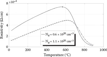
FIGURE 37.2 Calculated resistivity of silicon versus temperature, the two curves representing the upper and lower specification limits for the doping concentration of the PolyMUMPS process. The resistance of the polysilicon microbridge (Figure 37.1) would be proportional to these curves if the whole bridge could be at the same temperature. (Bao Quoc Ta et al., Electrical control of synthesis conditions for locally grown CNTs on polysilicon microstructure, 11th IEEE International Conference on Nanotechnology, August 15–18, 2011, Portland, Oregon, pp. 374–377. © (2011) IEEE. With permission.)
The individual grain resistivity, equivalent to the resistivity of single crystalline silicon, depends strongly on the temperature and the doping concentration [17, 18 and 19], as shown in Figure 37.2.
As the temperature increases, the resistivity increases due to the decrease in carrier mobility (thermal scattering), the density of charge carriers being fairly constant (equal to the doping density). However, when the temperature increases sufficiently, the number of charge carriers increases due to the thermal excitation of the electron–hole pairs. Above 550°C, the effect of increased conductivity due to these intrinsically excited charge carriers will dominate the effect of reduced mobility, causing a dramatic decrease in the resistivity as shown in Figure 37.2.
The temperature distribution of the microbridge when subject to resistive Joule heating, as obtained by a finite element method (FEM) simulation, is shown in Figure 37.3. The FEM model considers, as a simplification, only heat loss by conduction through the polysilicon microbridge to the substrate, neglecting other heat loss mechanisms (notably through convection). The doping level is assumed to be at the lower specified limit (cf. Figure 37.2). The parabolic-like distribution shows a temperature maximum (Tmax) near the center of the bridge, somewhat shifted away from the center due to the Thomson effect [20,21]. As CNTs are required to grow at the bridge center region, the highest temperature (Tmax) needs to be controlled.
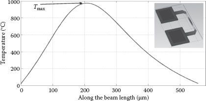
FIGURE 37.3 Simulation of temperature distribution of a polysilicon microbridge under Joule heating with Thomson effect. For a simplification, the simulation considers the heat loss only by conduction through the polysilicon microbridge to the anchors. (Bao Quoc Ta et al., Electrical control of synthesis conditions for locally grown CNTs on polysilicon microstructure, 11th IEEE International Conference on Nanotechnology, August 15–18, 2011, Portland, Oregon, pp. 374–377. © (2011) IEEE. With permission.)
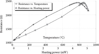
FIGURE 37.4 Total resistance of the bridge versus the highest temperature generated by Joule heating, and versus the heating power (COMSOL simulation). (Bao Quoc Ta et al., Electrical control of synthesis conditions for locally grown CNTs on polysilicon microstructure, 11th IEEE International Conference on Nanotechnology, August 15–18, 2011, Portland, Oregon, pp. 374–377. © (2011) IEEE. With permission.)
The resulting resistance of the microbridges under investigation was calculated by FEM (COMSOL). Figure 37.4 shows this resistance as a function of Tmax, and as a function of the corresponding heating power. The simulation considers only the ρg part in Equation 37.1, and takes into account the temperature-dependent resistivity (Figure 37.2) and the simulated temperature distribution caused by Joule heating (Figure 37.3).
37.3.2 EXPERIMENTAL CHARACTERIZATION
Figure 37.5 shows the measured resistance versus the applied heating power. The shape of the curve is qualitatively in accordance with the calculated curve in Figure 37.4. The higher power supply needed in the experiment, compared with the simulation, can be attributed to convection playing a role in the heat transfer from the microbridge. The relationship between resistance and temperature of the polysilicon structure is repeatable for every heating cycle after the first one. The first heating cycle serves as an annealing process that causes an increased grain size, reduced grain boundaries, and thus reduces and stabilizes the resistivity [21, 22 and 23]. Referring to Equation 37.1, this means that the system further approaches the limiting case where W ≪ L and δ ≪ L, where the simplification ρ ≈ ρg is valid. This implies that the released polysilicon bridges should be preheated to become predictable growth structures. The growth structure (center region of the microbridge) repeatedly reaches the desired temperature (850–950°C) when the overall resistance is about 1.5× the room temperature value (RT), whereas the maximum resistance value (1.63 × RT) occurs at a somewhat lower temperature. The temperature was determined experimentally, as a calibration, by using temperature-indicating paint (Tempilaq from Tempil, NJ, USA).
The desired synthesis temperature is at 900°C [1, 2 and 3]. This is in the range where the resistance decreases with increasing temperature (Figures 37.4 and 37.5). This causes challenges if the heating process is to be controlled using a voltage source, with stepwise increase in a controlled constant voltage. An increase of supplied voltage (V) would cause an additional increase in the Joule heating V2/R due to the simultaneous reduction of the resistance; hence, there is a positive feedback that eventually has been shown to destabilize the temperature.
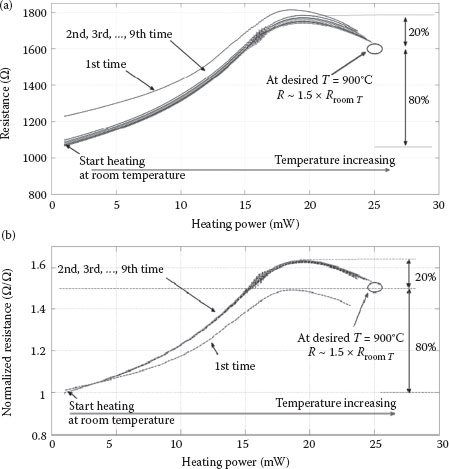
FIGURE 37.5 The total measured resistance (a) and normalized resistance (b) of the bridge versus the heating power. (Bao Quoc Ta et al., Electrical control of synthesis conditions for locally grown CNTs on polysilicon microstructure, 11th IEEE International Conference on Nanotechnology, August 15–18, 2011, Portland, Oregon, pp. 374–377. © (2011) IEEE. With permission.)
In this study, we controlled the heating process by supplied power instead of by supplied voltage. During the process, the measured resistance (R) is used to control the electric current (I) to keep the power (I2R), and thus the temperature at the desired value. This feedback control is done automatically using a LabView program. By using this method, we obtained stable temperature for the growth of CNTs. An artifact of this control method is shown in Figure 37.5: the resistance oscillation at the supplied heating power is ~16 mW. This is caused by a time delay in the heating power control, and the inherent strong increase in resistance at these temperatures. Since this artifact occurs at temperatures well below the desired growth temperature, it has no effect on the performance of our growth structure.
Figure 37.6 shows a scanning electron microscopy (SEM) image of a locally synthesized CNT connecting the two microbridges. CNTs grown appear straight across a gap of 15 μm, although the electric field in this study is 0.2 V/μm—about 10 times smaller than that discussed in Refs. [1,2].
We note that CNTs also grow in the opposite direction from the left side of the growth structure, shown in Figure 37.7, possibly influenced by the fringing electric field, as illustrated in Figure 37.8.
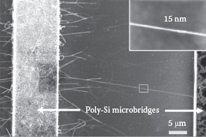
FIGURE 37.6 Locally synthesized CNT connecting two polysilicon microstructures. (Bao Quoc Ta et al., Electrical control of synthesis conditions for locally grown CNTs on polysilicon microstructure, 11th IEEE International Conference on Nanotechnology, August 15–18, 2011, Portland, Oregon, pp. 374–377. © (2011) IEEE. With permission.)
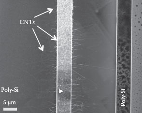
FIGURE 37.7 CNTs grown in the opposite direction, possibly due to the fringing electric field. (Bao Quoc Ta et al., Electrical control of synthesis conditions for locally grown CNTs on polysilicon microstructure, 11th IEEE International Conference on Nanotechnology, August 15–18, 2011, Portland, Oregon, pp. 374–377. © (2011) IEEE. With permission.)
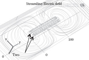
FIGURE 37.8 Simulation of the electric field between two microbridges (by COMSOL Multiphysics). (Bao Quoc Ta et al., Electrical control of synthesis conditions for locally grown CNTs on polysilicon microstructure, 11th IEEE International Conference on Nanotechnology, August 15–18, 2011, Portland, Oregon, pp. 374–377. © (2011) IEEE. With permission.)
On SEM inspection, Figures 37.9 and 37.10 show that the synthesized CNTs have a uniform and narrow distribution of CNT diameters (~80% in the range of 9–17 nm); and very high aspect ratios up to 1000:1 (length/diameter).
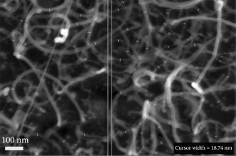
FIGURE 37.9 Measurement of the diameter of synthesized CNTs. (Bao Quoc Ta et al., Electrical control of synthesis conditions for locally grown CNTs on polysilicon microstructure, 11th IEEE International Conference on Nanotechnology, August 15–18, 2011, Portland, Oregon, pp. 374–377. © (2011) IEEE. With permission.)
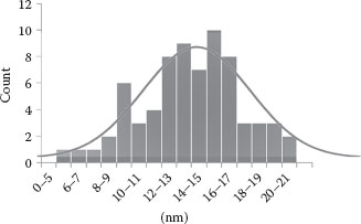
FIGURE 37.10 Distribution of the synthesized CNT diameters, for a random selection of CNTs. The solid line is a normal distribution of the same average and standard deviation. (Bao Quoc Ta et al., Electrical control of synthesis conditions for locally grown CNTs on polysilicon microstructure, 11th IEEE International Conference on Nanotechnology, August 15–18, 2011, Portland, Oregon, pp. 374–377. © (2011) IEEE. With permission.)
Current (I) −voltage (V) measurement is taken between the two microbridges. Figure 37.11 is the I −V curve of the sample in Figure 37.6 showing a fairly ohmic behavior, and an overall resistance of 400 kΩ. The present result is comparable with the previous results from refs. [1,2] (from 400 kΩ up to 6 MΩ).
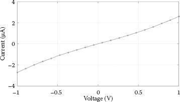
FIGURE 37.11 I −V curve of the bridging CNTs, shown in Figure 37.6, measured between two microbridges at room temperature, corresponding to an overall resistance of 400 kΩ. (Bao Quoc Ta et al., Electrical control of synthesis conditions for locally grown CNTs on polysilicon microstructure, 11th IEEE International Conference on Nanotechnology, August 15–18, 2011, Portland, Oregon, pp. 374–377. © (2011) IEEE. With permission.)
37.5 OUTLOOK AND POTENTIAL INDUSTRIAL IMPLEMENTATION
There is presently a very large interest in the integration of nanomaterials, and CNTs, in particular, in microsystems and microelectronics. This arises, on the one hand, from the unique properties of these nanomaterials:
• The nanoscale dimensions open up for miniaturization beyond what traditional microengineering can obtain, and beyond what is commonly regarded as physical limits for Si miniaturization.
• The huge surface-to-volume ratio of nanomaterials enables unsurpassed sensitivity in gas/chemical/biochemical sensing devices.
The other important reason for the importance of nanomaterial integration is that any device needs to interface with the macroscopic world. Microsystems and microelectronics can provide exactly this bridge between the nanomaterial and the macroscopic world, giving signal processing functionality, microfluid flow handling, actuation, and additional sensing capabilities on established manufacturing platforms.
Different methods for CNT integration in Si microsystems have been proposed and demonstrated, as outlined in the Introduction. The main benefits of the technique of direct integration by localized resistive heating is
• Localized CNT positions, integrating the CNTs where they are needed in active circuitry
• Low process temperature, being CMOS compatible
• Low cost
• Batch fabrication possibility
The goal will be to develop the process, so that it is fully compatible with the established industrial microengineering processes. As the industry heads toward heterogeneous integration, substantial effort is put into wafer-level integration of different technologies, in particular the integration of MEMS and CMOS technologies. Our demonstrated process may then be the last process step to add nano-functionality to the combined MEMS + CMOS wafers, potentially even including other types of technologies such as GaAs, SiC, and so on. We therefore regard this process as an important step toward realizing complete, integrated micro and nanosystems.
The main contributions from the work presented in this chapter are
• The demonstration of the direct integration process on a commercially available polysilicon platform (PolyMUMPS): This demonstrates that the process is compatible with standardized Si manufacturing processes, and that it does not rely on using more specialized and expensive technology platforms such as SOI.
• The technique of monitoring the temperature of the CNT growth structure through resistance measurements is important for the implementation in an industrial process. Previous techniques have involved analysis of the color of emitted light, requiring transparent windows in reactors and optical readouts that are not readily compatible with parallel batch manufacturing. The presently proposed technique using only electrical measurements is easily integrated in existing manufacturing platforms, allowing simultaneous monitoring of a large number of growth structures. It also opens up for easy automation of the process.
• The technique of controlling the temperature of the CNT growth structure through the temperature monitoring described above, and through the control of the supplied power, allows for a predictable and reliable control of the growth temperature, also in the temperature regions where the Si microbridge resistance decreases with the temperature. A reliable prediction and control of the synthesis temperature is essential for providing CNTs with the predictable properties and quality. Importantly, a temperature control based only on electrical measurements as outlined above is crucial for industrial implementation. Simultaneous control of the processing parameters for a large number of CNT growth structures can be realized without the need for expensive, dedicated equipment.
The work presented in this chapter therefore demonstrates the feasibility of the CNT direct integration process to be scaled up to an industrial compatible, wafer-level batch process at low cost, compatible with pre-processed wafers.
Our current work heads for an improved characterization and understanding of the growth process, where we aim at optimizing the process conditions for predictable and well-defined direct integration of CNTs in microsystems, as well as demonstration of sensor concepts.
We have demonstrated a process suitable for locally synthesizing and integrating CNTs on polysilicon structures at ambient temperature, thus showing compatibility with CMOS/MEMS technology. Our technique of monitoring the CNT synthesis temperature, which needs only the measurement of the growth structure electrical resistance, brings up a potential for an automated and mass production of CNT-integrated CMOS or MEMS devices. The method of controlling the synthesis temperature, by a feedback control to keep the supplied electrical power constant, tolerates the change in resistivity of polysilicon at elevated temperatures, thus keeping the synthesis process stable and well controlled. Our developments bring up the potential for the commercialization of synthesis and integration of CNTs into CMOS/MEMS devices.
The authors are grateful to Egil Erichsen and Bodil Holst, University of Bergen, Norway, for SEM imaging of samples.
1. D. Christensen, O. Englander, K. Jongbaeg, and L. Liwei, Room temperature local synthesis of carbon nanotubes, in Nanotechnology, 2003. IEEE-NANO 2003. 2003 Third IEEE Conference on, San Francisco, CA, August 12–14, 2003, vol. 2, pp. 581–584.
2. H. Chiamori, W. Xiaoming, G. Xishan, T. Bao Quoc, and L. Liwei, Annealing nano-to-micro contacts for improved contact resistance, in Nano/Micro Engineered and Molecular Systems (NEMS), 2010 5th IEEE International Conference on, Xiamen, China, January 20–23, 2010, pp. 666–670.
3. A. Jungen, C. Stampfer, J. Hoetzel, V. M. Bright, and C. Hierold, Process integration of carbon nanotubes into microelectromechanical systems, Sensors and Actuators A: Physical, 130–131, 588–594, 2006.
4. Z. Chen, J. Appenzeller, Y. -M. Lin, J. Sippel-Oakley, A. G. Rinzler, J. Tang, S. J. Wind, P. M. Solomon, and P. Avouris, An integrated logic circuit assembled on a single carbon nanotube, Science, 311, 1735, 2006.
5. R. F. Smith, T. Rueckes, S. Konsek, J. W. Ward, D. K. Brock, and B. M. Segal, Carbon nanotube based memory using CMOS production techniques, in Compound Semiconductor Integrated Circuit Symposium, 2006. CSIC 2006. IEEE, San Antonio, TX, November 12–15, 2006, pp. 47–50.
6. J. E. Jang, S. N. Cha, Y. Choi, G. A. J. Amaratunga, D. J. Kang, D. G. Hasko, J. E. Jung, and J. M. Kim, Nanoelectromechanical switches with vertically aligned carbon nanotubes, Applied Physics Letters, 87, 163114-3, 2005.
7. A. Star, K. Bradley, J.-C.P. Gabriel, and G. Gruner, Nano-electronic sensors: Chemical detection using carbon nanotubes, Polymeric Materials: Science & Engineering, 89, 204, 2003.
8. J. J. Brown, J. W. Suk, G. Singh, A. I. Baca, D. A. Dikin, R. S. Ruoff, and V. M. Bright, Microsystem for nanofiber electromechanical measurements, Sensors and Actuators A: Physical, 155, 1–7, 2009.
9. M. A. Cullinan and M. L. Culpepper, Design and fabrication of single chirality carbon nanotube-based sensors, in Nanotechnology (IEEE-NANO), 2011 11th IEEE Conference on, Portland, OR, August 15–19, 2011, pp. 26–29.
10. G. Qingqing, E. Albert, B. Fabel, A. Abdellah, P. Lugli, M. B. Chan-Park, and G. Scarpa, Solutionprocessable random carbon nanotube networks for thin-film transistors, in Nanotechnology (IEEE-NANO), 2011 11th IEEE Conference on, Portland, OR, August 15–19, 2011, pp. 378–381.
11. N. Patil, A. Lin, E. R. Myers, R. Koungmin, A. Badmaev, Z. Chongwu, H. S. P. Wong, and S. Mitra, Wafer-scale growth and transfer of aligned single-walled carbon nanotubes, Nanotechnology, IEEE Transactions on, 8, 498–504, 2009.
12. D. S. Engstrøm, N. L. Rupesinghe, K. B. K. Teo, W. I. Milne, and P. Bøgild, Vertically aligned CNT growth on a microfabricated silicon heater with integrated temperature control—Determination of the activation energy from a continuous thermal gradient, Journal of Micromechanics and Microengineering, 21, 015004, 2011.
13. S. Dittmer, S. Mudgal, O. A. Nerushev, and E. E. B. Campbell, Local heating method for growth of aligned carbon nanotubes at low ambient temperature, Low Temperature Physics, 34, 834–837, 2008.
14. S. Dittmer, O. A. Nerushev, and E. E. B. Campbell, Low ambient temperature CVD growth of carbon nanotubes, Applied Physics A: Materials Science & Processing, 84, 243–246, 2006.
15. F. Ding, K. Bolton, and A. Rosén, Nucleation and growth of single-walled carbon nanotubes: A molecular dynamics study, The Journal of Physical Chemistry B, 108, 17369–17377, 2004.
16. D. M. Kim, A. N. Khondker, S. S. Ahmed, and R. R. Shah, Theory of conduction in polysilicon: Driftdiffusion approach in crystalline-amorphous-crystalline semiconductor system. Part I: Small signal theory, Electron Devices, IEEE Transactions on, 31, 480–493, 1984.
17. G. W. Ludwig and R. L. Watters, Drift and conductivity mobility in silicon, Physical Review, 101, 1699–1701, 1956.
18. E. M. Conwell, Properties of silicon and germanium, Proceedings of the IRE, 40, 1327–1337, 1952.
19. J. E. Suarez, B. E. Johnson, and B. El-Kareh, Thermal stability of polysilicon resistors, Components, Hybrids, and Manufacturing Technology, IEEE Transactions on, 15, 386–392, 1992.
20. A. W. Van Herwaarden and P. M. Sarro, Thermal sensors based on the Seebeck effect, Sensors and Actuators, 10, 321–346, 1986.
21. G. R. Lahiji and K. D. Wise, A batch-fabricated silicon thermopile infrared detector, Electron Devices, IEEE Transactions on, 29, 14–22, 1982.
22. M. M. Mandurah, K. C. Saraswat, C. R. Helms, and T. I. Kamins, Dopant segregation in polycrystalline silicon, Journal of Applied Physics, 51, 5755–5763, 1980.
23. N. C. C. Lu, L. Gerzberg, and J. D. Meindl, A quantitative model of the effect of grain size on the resistivity of polycrystalline silicon resistors, Electron Device Letters, IEEE, 1, 38–41, 1980.
24. Bao Quoc Ta, N. Hoivik, E. Halvorsen, and K. E. Aasmundtveit, Electrical control of synthesis conditions for locally grown CNTs on polysilicon microstructure, 11th IEEE International Conference on Nanotechnology, August 15–18, 2011, Portland, Oregon, pp. 374–377.