
Solution-Processed Random Carbon Nanotube Networks Used in a Thin-Film Transistor |
CONTENTS
42.1 Carbon Nanotube Networks as Electronic Material
42.2 Random CNT Network Transistors
42.2.1 Fabrication of Random Network Transistors
42.2.2 Characterization of Random Network Transistors
42.2.3 Comparing Performance of Random Network Transistors
42.2.4 Simulating Nanotube Networks with a Percolation Model
42.1 CARBON NANOTUBE NETWORKS AS ELECTRONIC MATERIAL
The single-walled carbon nanotube (CNT) was discovered in 1993 [1], with a rolled graphene character [2]. Individual CNTs have a low density, high stiffness, and high axial strength [3]. CNT thin films exhibit superior visible and infrared optical transmittance comparable with the commercial indium tin oxide layer [4]. Depending on the chirality, single-walled CNTs can be either metallic or semiconducting [5]. As-grown CNTs contain both semiconducting and metallic species [6,7]. The metallic content can be eliminated by electrical breakdown [8] or by using density gradient sorting [9]. Semiconducting CNTs used in field-effect transistors exhibit near ballistic transport and high mobility [10,11]. The superior mechanical, optical, and electronic properties of CNTs make them attractive as emerging research material. In recent years, random CNT networks have been applied in high-frequency technique [12, 13 and 14], chemical and biosensing [15, 16 and 17], and in flexible and stretchable logic circuits [18, 19, 20, 21 and 22].
42.2 RANDOM CNT NETWORK TRANSISTORS
42.2.1 FABRICATION OF RANDOM NETWORK TRANSISTORS
Single-walled CNTs can be synthesized by arc-discharge, laser ablation, and chemical vapor deposition methods [23, 24 and 25]. Commercial CNTs are available in solid or liquid form from companies such as NanoIntegris and SWeNT. NanoIntegris CNTs are produced via arc-discharge and then purified with the density-gradient ultracentrifugation (DGU) method [9]. Separated CNTs with a semiconducting purity of up to 99% are available. The average tube diameter of NanoIntegris CNTs is ca.1.4 nm. The SWeNT CNTs are synthesized via an optimized chemical vapor deposition process, the CoMoCAT process, which provides CNTs with narrow chirality distribution peaked at (6,5) and (7,5) species [26]. As-grown nanotubes are purified by the DGU method with semiconducting content of around 90%. The average diameter of SWeNT CNTs is ca. 0.8 nm.
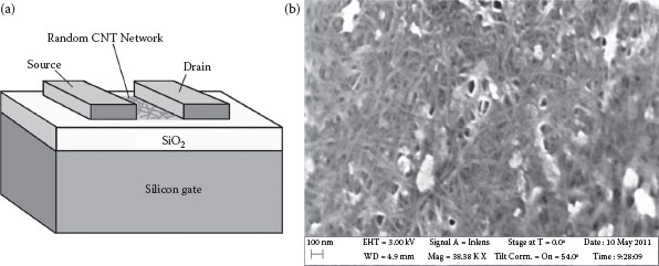
FIGURE 42.1 (a) SEM image of a CNT network deposited on a silicon substrate (SWeNT 90%-sc CNTs dissolved in NMP with a concentration of 10 μg/mL, scale bar: 100 nm). (b) Schematic diagram of a back-gated CNT network transistor. CNTs from the active channel between the source and drain contacts. The silicon substrate with an oxide layer serves as the back-gate. (From Q. Gong et al., 11th Proc. IEEE-Nano, Portland, pp. 378–381. Copyright 2011 IEEE, with permission.)
The solubility of single-walled CNTs in organic solvents is generally low. For instance, single-walled CNTs have room-temperature solubility of 10 μg/mL in N-methylpyrrolidinone (NMP) and 95 μg/mL in 1,2-dichlorobenzene (which is the highest solubility reported in Ref. [27]). Dispersion of single-walled CNTs in aqueous solution can be achieved with surfactants or biomolecules [28,29]. Surfactants can alter the electronic properties of CNTs, and therefore must be removed after deposition of nanotubes from solution to substrate. Commonly used surfactants include sodium dodecyl sulfate (SDS) and sodium cholate (SC) [9].
Random CNT networks can be deposited or transferred onto various substrates such as silicon wafer, quartz, glass, or flexible polymeric film. A monolayer such as 3-aminopropyltriethoxy-silane (APTES) can be applied to the substrate surface for improved adhesion and uniform distribution of the deposited nanotubes [30,31]. There are various coating techniques [32] for depositing CNTs from solution, such as dip coating [14], drop casting [33], spin coating [34], spray coating [35,36], inkjet printing [37], roll-to-roll printing [19], and transfer printing via polydimethysiloxane (PDMS) stamp or thermally activated adhesive tape [38,39]. Figure 42.1 shows an SEM image of a random CNT network drop-cast on an Si/SiO2 substrate.
When used as a conducting channel in thin-film transistors, the CNT networks must be effectively connected to the source and drain electrodes. For instance, conductive materials with similar composition, such as graphene [39] or metallic CNT films [19], have been reported for contacting semiconductor-enriched nanotube networks. Among metal contacts, palladium (Pd) is considered to be suitable due to its good wetting interaction combined with a high work function ΦPd = 5.1 eV [10,40]. A schematic diagram of a back-gated random network transistor is illustrated in Figure 42.1.
CNTs are distributed between and beneath the source/drain contacts. The silicon substrate with its thermal oxide layer serves as a global back gate. To achieve efficient gate control, a separate topgate needs to be built upon or under the network channel.
42.2.2 CHARACTERIZATION OF RANDOM NETWORK TRANSISTORS
Figure 42.2 shows the I–V characteristics of a back-gated random network transistor. The output characteristics ID–VDS were measured at VGS from −4 V to + 4 V in 2 V steps. The saturation of the drain currents at high drain voltage can be seen in the left subfigure. The drain conductance gD can be calculated from the output curves using Equation 42.1. The effective mobility μeff is determined by gD with Equation 42.2, where L is the channel length, W is the channel width, Vth is the threshold voltage, and Cox is the oxide capacitance [41].
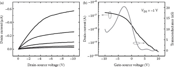
FIGURE 42.2 I–V characteristics of a back-gated random network transistor on a silicon wafer with 200 nm SiO2, contacted with 10 nm Pd/30 nm Au electrodes. The channel geometry is L = 100 μm, W = 1000 μm. NanoIntegris 98%-sc CNTs was dissolved in NMP with a concentration of 2.5 μg/mL). (a) Output characteristics ID – VDS, measured at VGS = −4 V to + 4 V in 2 V steps (from top to bottom). (b) Transfer characteristic ID – VGS and the transconductance gm, measured at fixed drain-source voltage VDS = −1 V.
Figure 42.2 also shows the drain current ID and transconductance gm as a function of the gate-source voltage VGS, measured at VDS = −1 V. From the transfer curve, the on- and off-currents are defined as the drain current at the on- and off-states of the transistor, and the on/off ratio is the ratio of these. For the random CNT network transistors, the maximum on/off ratio has been reported to exceed 105 [22], which is smaller than the ratio of transistors with individual CNTs as an active channel. The ratio of random network transistors depends on the channel material and on the channel length, and is limited by the presence of metallic tubes in the network, which results in a high off-current.
The transconductance gm is defined by Equation 42.3. Using Equation 42.4, the field-effect mobility μFE can be derived from gm [41,42]. The carrier mobility determines the carrier velocity, and hence the switching speed [11]. Generally, the field-effect mobility μFE is smaller than the effective mobility μeff for the same device, although μFE is commonly used [41]. The gate capacitance per unit area Cox can be derived from two models. The parallel plate model treats the active channel material as a uniform sheet and depends only on the dielectric material (oxide in this case) thickness tox, and the dielectric constant εox, as given in Equation 42.5. For SiO2, the oxide dielectric constant εox = 3.9, so that the gate capacitance of the 200 nm SiO2 layer is calculated to be Cox = 17.26 nF/cm2. Equation 42.6 is a modified array model, which includes the influence of the average spacing between nanotubes, defined as Λ0 [43]. The quantum capacitance of CNT is CQ = 4.0 × 10⁻¹⁰ F/m [21]. R is the mean radius of the CNTs. As the nanotube density increases, the modified array model approaches the parallel plate model. At sufficient high nanotube density, the difference between the two models is negligible.
(42.1) |
(42.2) |
(42.3) |
(42.4) |
(42.5) |
(42.6) |
42.2.3 COMPARING PERFORMANCE OF RANDOM NETWORK TRANSISTORS
In our previous study [33], we built various kinds of random CNT network transistors and studied the effect on performance metrics such as the on/off ratio and field-effect mobility of device parameters such as the network density, the band gap, and the degree of semiconductor enrichment. Single-walled CNTs were purchased from SWeNT (90%-sc, mean diameter 0.8 nm) and from NanoIntegris (98%-sc, mean diameter 1.4 nm). CNTs were dissolved in NMP without additional surfactants. Random nanotube networks were then constructed by drop-casting nanotube suspension on the Si/SiO2 substrate. The network density was controlled by varying the suspension concentration from 1.25 to 10 μg/mL, as well as by multiple casting of the 10 μg/mL suspension to achieve high network density.
Figure 42.3 summarizes the results of the performance comparison. Generally, the on/off ratio decreases with increasing network density due to the increase of metallic content in the nanotube network, which leads to a more rapid rise of the off-current than the on-current. The field-effect mobility increases with increasing network density, although this trend saturates above a certain density threshold, as shown in Figure 42.3. This is presumably due to the preferential charge transport through the metallic nanotube network at high density, which dilutes the contribution of the semiconducting network to the channel conductance, with a corresponding reduction in the transconductance of the channel and in the field-effect mobility.
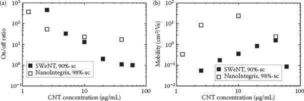
FIGURE 42.3 Performance (a) on/off ratio; (b) field-effect mobility (μFE) of the SWeNT (90%-sc) and NanoIntegris (98%-sc) CNTs-based field-effect transistors versus network density. The network density is parameterized by the concentration of the CNT/NMP suspension, from which the CNT networks were deposited. (From Q. Gong et al., 11th Proc. IEEE-Nano, Portland, pp. 378–381. Copyright 2011 IEEE, with permission.)
The band gap of semiconducting CNTs scales inversely with the tube diameter [44], so that the SWeNT CNTs have a larger band gap than the NanoIntegris nanotubes. The large band gap results in a lower conductivity of the semiconducting nanotubes and, consequently, a lower charge mobility, as shown in Figure 42.3. Owing to the much higher metallic content (10% metallic), the SWeNT nanotube-based network transistors have a substantially lower on/off ratio than the NanoIntegris (2% metallic) nanotube-based network transistors for the high network density devices. At a low network density, semiconducting nanotubes dominate the charge transport of both sets of devices. The higher on/off ratio of the low-density SWeNT devices than NanoIntegris devices is due to the larger band gap of the SWeNT nanotubes.
42.2.4 SIMULATING NANOTUBE NETWORKS WITH a PERCOLATION MODEL
To understand the correlation between the electrical characteristics and the geometrical properties of CNT networks, a Monte Carlo-based method can be applied to simulate the networks of randomly distributed single-walled CNT networks [45,46]. The generated thin films are confined to a 3D box of dimensions L × W × H, where L,W, and H are the length, width, and height. The CNTs within this volume are modeled as cylinders with length LCNT and diameter dCNT. The electrodes are represented by metallic tubes positioned in the two opposite defined regions of the 3D box (Figure 42.4).
The orientation of CNTs inside the defined volume is determined by two angles α ∈ [0, π], the angle between the nanotube axis and the plane of the active channel, and β ∈ [0, π], the angle between the nanotube axis and the direction of current flow. The length of each CNT as well as its diameter are sampled from a log-normal distribution [47, 48 and 49]. The CNTs are generated and placed randomly inside the given volume so that at least one end of each nanotube lies inside the 3D box. CNTs are randomly generated until a given total tube number or a desired density is reached. For each network, a finite range of chiral indices (n,m) can be specified for the generated CNTs. CNTs are either metallic or semiconducting, depending on the chiral indices. After network generation, redundant nanotubes which do not contribute to a percolation path (a continuous chain of nanotubes) between the electrodes are removed. Next, the tube–tube junctions are calculated. The junction points between two CNTs can be metallic–metallic (MM), semiconducting–semiconducting (SS), or metallic–semiconducting (MS). The resistance of conducting CNTs is about 6 kΩ/μm of nanotube length. The resistance of metallic nanotubes can be calculated using Equation 42.7 with a mean tube length LCNT = 1 μm [47].
(42.7) |
The resistances of intertube junctions are considered to follow a normal distribution. The homogeneous junctions (MM- or SS-type) have a resistance that ranges between a minimum value of 180 kΩ and a maximum value of 420 kΩ. The resistances of heterogeneous junctions (MS-type) are considered to be a hundred times larger than homogeneous junctions, between 18 and 42 MΩ, as reported in Ref. [48]. After generation of the nanotube network and determination of the junction resistances, the network is converted to a simulation program with integrated circuit emphasis (SPICE)-compatiable circuit file and the total current across the thin film is calculated with HSPICE.
Figure 42.4 shows the conductance of simulated nanotube networks as a function of network density. The channel length L was fixed and two channel widths, W = L and W = 2L, were modeled. The increase of the semiconducting content in the nanotube network from 70% (as-grown) to 90% (separated), with the same channel geometry, leads to a decreased off-current, indicated by the reduced conductance at VGS = 0 V. The conductance increases with increasing network density, as more nanotubes contribute to the formation of percolation paths between the electrodes. Decreasing the channel length significantly increases the probability of forming percolation paths between electrodes. For an optimum design, the channel length should be short enough to allow the formation of semiconducting percolating paths with a small amount of nanotubes in order to keep the metallic network sparse, while keeping a minimum length in order to minimize the influence of metallic paths.
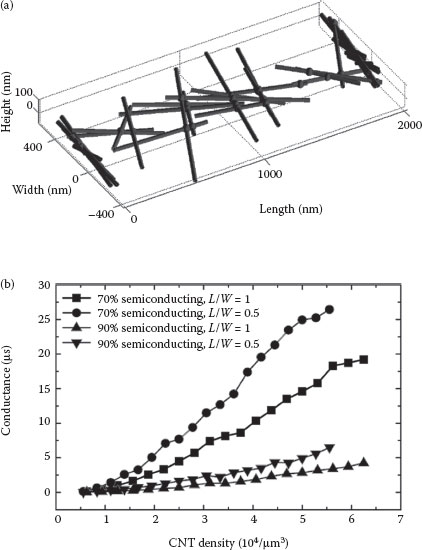
FIGURE 42.4 (a) An example of a randomly generated 3D CNT network. Metallic nanotubes were randomly placed with defined content in the nanotube network. (b) Comparison of conductance at different nanotube densities for random CNT networks with 70% and 90% semiconducting contents with channel geometries: L/W = 0.5 and 1. VDS = −5 V and VGS = 0 V. (From Q. Gong et al., 11th Proc. IEEE-Nano, Portland, pp. 378–381. Copyright 2011 IEEE, with permission.)
Single-walled CNTs are promising novel materials with superior electronic, mechanical, and optical properties. Solution-processable random CNT networks are easy to manipulate. They can be produced at ambient pressure and room temperature with a low cost and high yield. However, the performance of random CNT network transistors is so far not competitive with traditional siliconbased devices. The potential application of random carbon networks may first be realized in novel devices such as chemical biosensors, because the cylindrical nanometer scale structure of CNTs can be readily attached by molecules. The chemical inertia, the stability in the ambient environment, and the sensitivity of CNTs enable reliable and sensitive sensing processes. Another possibility may be in ultra-high-frequency applications due to the ballistic transport inside CNTs. Recently, random CNT network transistors have been integrated in flexible stretchable circuits, with potential applications in electronic textiles and artificial skin.
There are several challenges for future applications of CNT devices. Purer and more homogeneous nanotube samples with narrow chirality and diameter distributions, high purity of electronic type (semiconducting vs. metallic), and precise doping are needed. Scalable precision methods are needed for oriented nanotube network deposition with controlled density and alignment. Finally, efficient gate dielectric and gate metal, and low resistance contact are demanded for high-performance electronics.
This work was sponsored by the German Research Foundation (DFG) through the TUM International Graduate School of Science and Engineering (IGSSE) and the TUM Institute for Advanced Studies (IAS).
1. S. Iijima and T. Ichihashi, Single-shell carbon nanotubes of 1-nm diameter, Nature, 363, 603–605, 1993.
2. P. Avouris, Z. Chen, and V. Perebeinos, Carbon-based electronics, Nat. Nanotechnol., 2, 605–615, 2007.
3. M. Treacy, T. Ebbesen, and J. Gibson, Exceptionally high Young’s modulus observed for individual carbon nanotubes, Nature, 381, 678–680, 1996.
4. Z. Wu, Z. Chen, X. Du, J. Logan, J. Sippel, M. Nikolou, K. Kamaras, J. Reynolds, D. Tanner, A. Hebard, and A. Rinzler, Transparent, conductive carbon nanotube films, Science, 305, 1273–1276, 2004.
5. J. Wildöer, L. Venema, A. Rinzler, R. Smalley, and C. Dekker, Electronic structure of atomically resolved carbon nanotubes, Nature, 391, 59–62, 1998.
6. K. Yanagi, Y. Miyata, T. Tanaka, S. Fujii, D. Nishide, and H. Kataura, Colors of carbon nanotubes, Diam. Relat. Mater., 18, 935–939, 2009.
7. L. Huang, H. Zhang, B. Wu, Y. Liu, D. Wei, J. Chen, Y. Xue, G. Yu, H. Kajiura, and Y. Li, A generalized method for evaluating the metallic-to-semiconducting ratio of separated single-walled carbon nanotubes by UV-vis-NIR characterization, J. Phys. Chem. C., 114, 12095–12098, 2010.
8. P. Collins, M. Arnold, and P. Avouris, Engineering carbon nanotubes and nanotube circuits using electrical breakdown, Science, 292, 706–709, 2001.
9. M. Arnold, A. Green, J. Hulvat, S. Stupp, and M. Hersam, Sorting carbon nanotubes by electronic structure using density differentiation, Nat. Nanotechnol., 1, 60–65, 2006.
10. A. Javey, J. Guo, Q. Wang, M. Lundstrom, and H. Dai, Ballistic carbon nanotube field-effect transistors, Nature, 424, 654–657, 2003.
11. T. Dürkop, S. Getty, E. Cobas, and M. Fuhrer, Extraordinary mobility in semiconducting carbon nanotubes, Nano Lett., 4, 35–39, 2004.
12. C. Rutherglen, D. Jain, and P. Burke, Nanotube electronics for radiofrequency applications, Nat. Nanotechnol., 4, 811–819, 2009.
13. L. Nougaret, H. Happy, G. Dambrine, V. Derycke, J. Bourgoin, A. Green, and M. Hersam, 80 GHz field-effect transistors produced using high purity semiconducting single-walled carbon nanotubes, Appl. Phys. Lett., 94, 243505, 2009.
14. C. Wang, A. Badmaev, A. Jooyaie, M. Bao, K. Wang, K. Galatsis, and C. Zhou, Radio frequency and linearity performance of transistors using high-purity semiconducting carbon nanotubes, ACS Nano, 5, 4169–4176, 2011.
15. J. Novak, E. Snow, E. Houser, D. Park, J. Stepnouski, and R. McGill, Nerve agent detection using networks of single-walled carbon nanotubes, Appl. Phys. Lett., 83, 4026–4028, 2003.
16. J. Li, Y. Lu, Q. Ye, M. Cinke, J. Han, and M. Meyyappan, Carbon nanotube sensors for gas and organic vapor detection, Nano Lett., 3, 929–933, 2003.
17. G. Gruner, Carbon nanotube transistors for biosensing applications, Anal. Bioanal. Chem., 384, 322–335, 2006.
18. Q. Cao, H. Kim, N. Pimparkar, J. Kulkarni, C. Wang, M. Shim, K. Roy, M. Alam, and J. Rogers, Medium-scale carbon nanotube thin-film integrated circuits on flexible plastic substrates, Nature, 454, 495–500, 2008.
19. M. Jung, J. Kim, J. Noh, C. Lim, G. Lee, J. Kim, H. Kang et al., All-printed and roll-to-roll-printable 13.56-MHz-operated 1-bit RF tag on plastic foils, IEEE T. Electron. Dev., 57, 571–580, 2010.
20. S. Kim, S. Kim, J. Park, S. Ju, and S. Mohammadi, Fully transparent pixel circuits driven by random network carbon nanotube transistor circuitry, ACS Nano, 4, 2994–2998, 2010.
21. T. Takahashi, K. Takei, A. Gillies, R. Fearing, and A. Javey, Carbon nanotube active-matrix backplanes for conformal electronics and sensors, Nano Lett., 11, 5408–5413, 2011.
22. D. Sun, M. Timmermans, Y. Tian, A. Nasibulin, E. Kauppinen, S. Kishimoto, T. Mizutani, and Y. Ohno, Flexible high-performance carbon nanotube integrated circuits, Nat. Nanotechnol., 6, 156–161, 2011.
23. H. Dai, Nanotube growth and characterization, Topics Appl. Phys., 80, 29–53, 2001.
24. C. Journet, W. Maser, P. Bernier, A. Loiseau, M. de la Chapelle, S. Lefrant, P. Deniard, R. Lee, and J. Fisher, Large-scale production of single-walled carbon nanotubes by the electric-arc technique, Nature, 388, 756–758, 1997.
25. C. Scott, S. Arepalli, P. Nikolaev, and R. Smalley, Growth mechanisms for single-wall carbon nanotubes in a laser-ablation process, Appl. Phys. A, 72, 573–580, 2001.
26. S. Bachilo, L. Balzano, J. Herrera, F. Pompeo, D. Resasco, and R. Weisman, Narrow (n,m)-distribution of single-walled carbon nanotubes grown using a solid supported catalyst, J. Am. Chem. Soc., 125, 11186–11187, 2003.
27. J. Bahr, E. Mickelson, M. Bronikowski, R. Smalley, and J. Tour, Dissolution of small diameter single-wall carbon nanotubes in organic solvents, Chem. Commun., 2, 193–194, 2001.
28. R. Haggenmueller, S. Rahatekar, J. Fagan, J. Chun, M. Becker, R. Naik, T. Krauss et al., Comparison of the quality of aqueous dispersions of single wall carbon nanotubes using surfactants and biomolecules, Langmuir, 24, 5070–5078, 2008.
29. D. Jain, N. Rouhi, C. Rutherglen, C. Densmore, S. Doorn, and P. Burke, Effects of source, surfactant, and deposition process on electronic properties of nanotube arrays, J. Nanomater., 2011, 174268, 2010.
30. R. Krupke, S. Malik, H. Weber, O. Hampe, M. Kappes, and H. Löhneysen, Patterning and visualizing self-assembled monolayers with low-energy electrons, Nano Lett., 2, 1161–1164, 2002.
31. M. Vosgueritchian, M. LeMieux, D. Dodge, and Z. Bao, Effect of surface chemistry on electronic properties of carbon nanotube network thin film transistors, ACS Nano, 4, 6137–6145, 2010.
32. F. Krebs, Fabrication and processing of polymer solar cells: A review of printing and coating techniques, Sol. Energ. Mat. Sol. C., 93, 394–412, 2009.
33. Q. Gong, E. Albert, B. Fabel, A. Abdellah, M. Chan-Park, P. Lugli, and G. Scarpa, Solution-processable random carbon nanotube networks for thin-film transistors, in Proc. 11th IEEE-Nano, Portland, pp. 378–381, 2011.
34. M. Roberts, M. LeMieux, A. Sokolov, and Z. Bao, Self-sorted nanotube networks on polymer dielectrics for low-voltage thin-film transistors, Nano Lett., 9, 2526–2531, 2009.
35. E. Bekyarova, M. Itkis, N. Cabrera, B. Zhao, A. Yu, J. Gao, and R. Haddon, Electronic properties of single-walled carbon nanotube networks, J. Am. Chem. Soc., 127, 5990–5995, 2005.
36. W. Wong and A. Salleo, Flexible Electronics: Materials and Applications. New York, NY: Springer, 2009, Chapter 10.
37. P. Chen, Y. Fu, R. Aminirad, C. Wang, J. Zhang, K. Wang, K. Galatsis, and C. Zhou, Fully printed separated carbon nanotube thin film transistor circuits and its application in organic light emitting diode control, Nano Lett., 11, 5301–5308, 2011.
38. Y. Zhou, L. Hu, and G. Grüner, A method of printing carbon nanotube thin films, Appl. Phys. Lett., 88, 123109, 2006.
39. S. Jang, H. Jang, Y. Lee, D. Suh, S. Baik, B. Hong, and J. Ahn, Flexible, transparent single-walled carbon nanotube transistors with graphene electrodes, Nanotechnology, 21, 425201, 2010.
40. Z. Chen, J. Appenzeller, J. Knoch, Y. Lin, and P. Avouris, The role of metal-nanotube contact in the performance of carbon nanotube field-effect transistors, Nano Lett., 5, 1497–1502, 2005.
41. D. Schroder, Semiconductor Material and Device Characterization. New York, NY: John Wiley & Sons, 1998, Chapter 8.
42. F. Schwierz, Graphene transistors, Nat. Nanotechnol., 5, 487–496, 2010.
43. Q. Cao, M. Xia, C. Kocabas, M. Shim, and J. Rogers, Gate capacitance coupling of single-walled carbon nanotube thin-film transistors, Appl. Phys. Lett., 90, 023516, 2007.
44. M. O’Connell, Carbon Nanotubes: Properties and Applications. New York, NY: Taylor & Francis Group, 2006, Chapter 4.
45. A. Behnam and A. Ural, Computational study of geometry-dependent resistivity scaling in single-walled carbon nanotube films, Phys. Rev. B, 75, 125432, 2007.
46. J. Hicks, A. Behnam, and A. Ural, Resistivity in percolation networks of one dimensional elements with a length distribution, Phys. Rev. E, 79, 012102, 2009.
47. L. Hu, D. Hecht, and G. Gruener, Carbon nanotube thin films: Fabrication, properties, and applications, Chem. Rev., 110, 5790–5844, 2010.
48. D. Jack, C. Yeh, Z. Liang, S. Li, J. Park, and J. Fielding, Electrical conductivity modeling and experimental study of densely packed SWCNT networks, Nanotechnology, 21, 195703, 2010.
49. R. Tenent, T. Barnes, J. Bergeson, A. Ferguson, B. To, L. Gedvilas, M. Heben, and J. Blackburn, Ultrasmooth, large-Area, high-uniformity, conductive transparent single-walled-carbon-nanotube films for photovoltaics produced by ultrasonic spraying, Adv. Mater., 21, 3210–3216, 2009.