
CONTENTS
61.2 NML Components of the Full Adder
61.2.2 Programmability and Majority Gate
61.2.4 Shape Engineering: Asymmetric Nanomagnets
61.4 Fabrication and Characterization
61.5 Proposed Designs of Full Adder
The development and characterization of a nanomagnet full adder circuit are demonstrated in this chapter. To our knowledge, this is the most complex magnetic circuit attempted to date. The circuit comprises 53 magnets that perform as three majority gates plus internal interconnections, with only one internal error. The inputs of the gate can be set independently, allowing an exhaustive test of the magnetic operation. We introduce two other different designs of a full adder circuit built from nanomagnets. We use previously demonstrated and tested nanomagnet logic (NML) components, such as inverters, wires [1], programmable inputs [2], shape-engineered magnets [3], and fanouts [4], to realize a larger-scale circuit.
NML is a novel nanoscale computing paradigm where circuits are constructed from sub-100 nm, single-domain magnets. Logic signals are propagated in magnetic “wires” built from nanomagnets placed side by side. The emanating magnetic field of a magnet provides the interaction. NML technology is receiving increasing attention due to its special benefits, such as low power dissipation with high integration density of functional devices, operation over a wide range of temperatures, and nonvolatility [5].
The basic unit of NML is the nanomagnet, as shown in the schematic of Figure 61.1, as a rectangle. It is well known that a symmetrically shaped magnet has an energy barrier between two stable states, as shown in Figure 61.1, with the energy (E) versus magnetization (H) landscape as shown. Consider a symmetric magnet that is subjected to a strong hard-axis field (indicated by the thick blue arrow pointing from left to right in Figure 61.1). For a large hard-axis external field, referred to as the “clocking field,” the magnetization is pointing in the direction of the field, and favors neither the up nor the down direction, a condition referred to as “nulled.” When the field is removed, the nanomagnet relaxes into one of the two energetically equivalent ground states, that is, pointing either up or down. Even a small biasing field along the easy axis can influence which magnet ground state the magnetization will select. In Figure 61.1, the blue curve shows the potential landscape of the nanomagnet immediately after the removal of the nulling field. The presence of the energy barrier requires that an external field stronger than the nulling field is required to reevaluate the magnet, that is, set the magnet so that a new logic value, either up or down, can be written to it. It relaxes into a newly ordered state, in accordance with any present biasing field. The magnet retains its new state without an externally applied field, since the size of the magnet is assumed to be larger than the superparamagnetic limit.
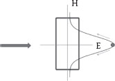
FIGURE 61.1 Energy landscape and clocking process of a symmetric, rectangular-shaped nanomagnet. The thick, horizontal, blue arrow indicates the strong hard-axis clocking field. As the field is removed, the symmetric nanomagnet relaxes into one of the two energetically equivalent ground states.
61.2 NML COMPONENTS OF THE FULL ADDER
All NML circuits are built from closely spaced nanomagnets, and are constructed in such a way that the magnets are located on a grid-based array, that is, they form horizontal and vertical lines in a plane. Various basic structures are necessary to build a complex NML circuit. NML devices are interconnected by magnetic “wires,” which in the case of NML refers to a line of nanomagnets along which the signal is propagated. The basic logic element of the currently existing NML library is the majority gate in which one magnet reflects the total magnetic forces of the surrounding magnets. Signal distribution, that is, fanout, is performed by splitting the input signal and passing on as three output signals. Above all, shape engineering helps to design programmable inputs as well as to reduce the overall footprint. All these components are described in the following sections.
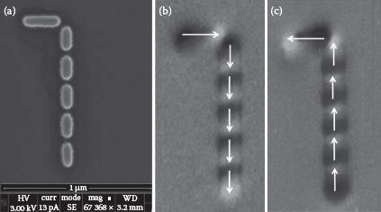
Nanomagnets comprising NML wires can be coupled in one of two ways. One of these is the vertically aligned wire with ferromagnetically coupled (FC) magnets, and the other is the horizontally aligned wire built from antiferromagnetically coupled (AFC) magnets. Figure 61.2a is a scanning electron micrograph (SEM) of a typical vertically aligned wire. The one horizontally aligned magnet on the top is the “driver” magnet; it initializes the entire wire through FC. Figures 61.2b and 61.2c are magnetic force microscope (MFM) images showing the magnetic state of all the magnets in the wire.
One horizontally aligned, five-magnet-long wire is shown in Figure 61.3a. Here, the information propagates from the horizontal driver magnet through the AFC magnets, that is, from left to right. Two MFM images (Figures 61.3b and 61.3c) show the magnetization of the same wire for two possible states of the driver magnet.
61.2.2 PROGRAMMABILITY AND MAJORITY GATE
Most NML designs use magnets with a rounded-edge rectangular shape, as shown in the previous figures. Magnets with different aspect ratios can enhance logic functionality, as summarized in Ref. [2]. The switching field required to reverse the magnetization coercivity along the long axis increases with its length. This phenomenon has been used in the programmable majority gates [3] shown in Figure 61.4. The majority gate is the basic logic structure of NML because influence by fixing one of the inputs, it can take on the roles of the AND and OR gates [1]. The three horizontal driver magnets have different aspect ratios, enabling programmability of the logic gate. Programmability is achieved using external fields with various strengths, such that the longest driver magnet is set at the highest field, and subsequent lower fields set shorter driver magnets. The driver magnets set the “input” magnets through FC. The center magnet is the “compute” magnet, which responds to the total magnetic force of all three input magnets in a majority fashion. The compute magnet influences the “output” magnet through AFC. All eight input combinations are shown in Figure 61.5 for the same gate.
FIGURE 61.2 (a) SEM image of a five-nanomagnet-long vertical wire with a horizontally aligned driver magnet. (b) MFM image of the same wire for one magnetization state of the driver magnet and (c) for the other. The information propagates from the driver magnet toward the bottom of the wire by ferromagnetic coupling.
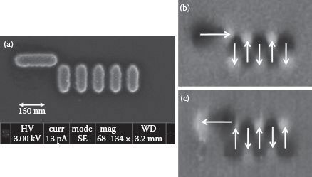
FIGURE 61.3 (a) SEM image of a five-nanomagnet-long horizontal wire with a horizontally aligned driver magnet. (b) MFM image of the same wire for one magnetization state of the driver magnet and (c) for the other. The horizontal driver magnet initializes the entire wire, thereby defining the magnetization state of all the magnets. The information propagates from left to right, that is, from the region of the strongest influence to the region of the weakest influence.
In addition to the NML structures discussed above, nanomagnet fanout is also necessary to construct large circuits such as an NML full adder. The aspect-ratio-dependent switching phenomenon has been exploited for the design of the fanout structures [4] as well to provide a stable input for magnetic circuits. A fanout structure is shown in Figure 61.6 with the schematic (Figure 61.6a) and the SEM image (Figure 61.6b). Two MFM images summarize the magnetization of the same structure shown in the SEM according to the two possible magnetization states of the vertical driver magnet.
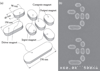
FIGURE 61.4 (a) Schematic of the majority gate with various shapes of the driver magnets providing signals to the input bits. (b) SEM of the fabricated permalloy structure.
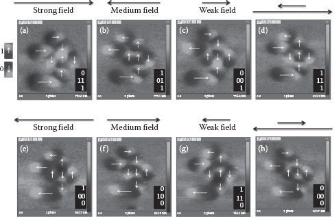
FIGURE 61.5 MFM images of the programmable majority gate for all input combinations. The black insets show the three input values along the output, majority value. Note that because the middle input is AFC to the compute magnet, its physical orientation results in the opposite logic value compared with the other two inputs, that is, down is logic “1.”
Elongation of the driver magnet allows it to be set at a higher external field while the rest of the fanout circuit is nulled at a lower field without causing the driver to change its state.
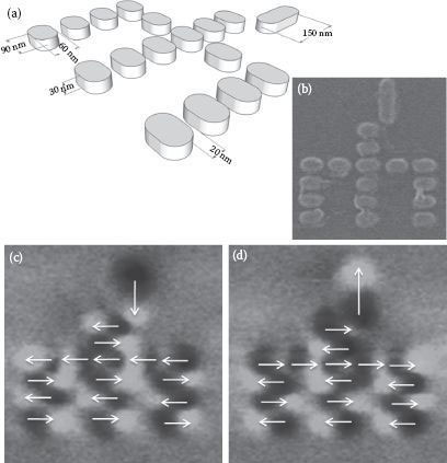
FIGURE 61.6 (a) Schematic, (b) SEM, and (c), (d) MFM images for both possible driver magnetization states of the fanout circuit.
61.2.4 SHAPE ENGINEERING: ASYMMETRIC NANOMAGNETS
Shapes other than oval have been investigated in Refs. [6,7], where the nanomagnets are asymmetric, having a slanted edge, as shown in Figure 61.7 on the left side. Simulations based on the single-domain model show that the asymmetry of the magnet shifts the entire energy landscape of the magnet, whereby the energy minima are shifted as well. The thin line along the diagonal of the magnet in Figure 61.8 corresponds to the effective easy axis. The energy maximum is perpendicular to this axis. The horizontally applied field is not precisely in the direction of the energy maximum, so the resulting energy of the magnet is to one side of the maximum and falls toward the appropriate ground state when the field is removed. As a result of the tilted easy axis, the nanomagnet takes on a preferred magnetization direction, as summarized in Figure 61.8.
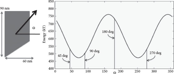
FIGURE 61.7 Schematic of the slant magnet (left) and simulation result based on the single-domain model for the slant nanomagnet energy landscape. The energy minima are shifted from the long geometrical axis, that is, from the 90° and 270° magnetization direction.
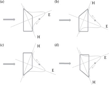
FIGURE 61.8 Energy curves of the slant magnets for different slant locations. The external magnetic field is applied from left to right shown by horizontal, thick, blue arrows. The thin line along the diagonal of the magnet corresponds to the effective easy axis. The energy maximum is perpendicular to this axis.
The schematic lists all possible slant orientations and the corresponding overlaid energy diagrams, energy (E) versus magnetization (H). The magnets in (a) and (d) relax into the downward pointing magnetization, and in (b) and (c) relax into the upward pointing direction. This specific shape can be exploited to reduce the device footprint as shown below.
The logic structures described above, as well as those previously published [8,9], have a relatively basic level of complexity; one structure had one basic function (AND/OR/majority). Prior to this study, the total number of inputs was a maximum of three with one single compute nanomagnet (majority gate), and the information was passed along a few-magnet-long magnetic wire, or fanned out with a few wires. The total number of magnets was low as well. In the case of the full adder, the basic, most simple circuit design would include multiple logic gates, such as the AND and OR gates. Since the fundamental building block of NML is the majority gate, upon which the AND and OR gates are based, it is not efficient to restrict the functionality to the AND/OR functions since considerable space is wasted with the extra inputs and associated magnets. Rather, it is better to find a circuit design constructed from majority gates from which it is straightforward to realize the full adder directly. Such a design of the full adder was proposed in Ref. [10] proving the operation using five three-input majority gates (Figure 61.9a). A smaller design was introduced later in Refs. [11,12] where the circuit is composed of only three three-input majority gates (Figure 61.9b).
More complicated designs were published that required one three-input majority gate and one five-input majority gate [13]. Since the three-input nanomagnet majority gate was tested successfully in Refs. [1,5], we chose them to construct the full adder of Figure 61.9b instead of the one with five inputs. Figure 61.10 shows a possible nanomagnet-based layout with three three-input majority gates (the cross point of the horizontal and the vertical nanomagnet wires) built in [14]. Each input is applied at multiple positions in the circuits of Figure 61.10, making it possible to implement the layout without wire crossings.
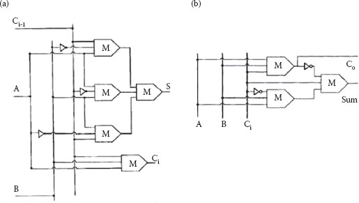
FIGURE 61.9 (a) An early full adder design constructed from five majority gates (E. Varga et al., Experimental demonstration of non-majority, nanomagnet logic gates, IEEE DRC (Device Research Conference) Technical Digest, pp. 87–88, © (2010) IEEE. With permission.) and (b) the smaller full adder design proposed in several publications (W. Wang, K. Walus and G. A. Jullien, Quantum-dot cellular automata adders, 3rd IEEE Conference on Nanotechnology, 1–2, 461–464, © (2003) IEEE. H. Cho and E. E. Swartzlander, Adder designs and analyses for quantum-dot cellular automata, IEEE Transactions on Nanotechnology, 6(3), 374–383, © (2007) IEEE. With permission.). Only three majority voting gates are necessary for the full adder implementation. Since the AFC wire comprises a series of inverters, depending on the total length being an even or odd number of magnets, the inverter function is included in the wire length.
The long magnets on the left side of the circuit in Figure 61.10 are the programmable drivers providing the data for testing the adder. A particular Bext applied field can switch only magnets with a switching field (coercivity) Bsw < Bext. Higher aspect ratios yield higher switching fields. Therefore, a globally applied magnetic field can switch only magnets smaller than a certain length. Figure 61.11 shows the calculated [15] switching field of several different-sized magnets. The thicknesses of the magnets are 20 and 30 nm, their width is fixed at 60 nm, and the coercivity is plotted as the function of their length. The field is applied at a 45° angle to the long axis of the magnets. Exploiting the aspect ratio as a design variable, the driver magnets can be set separately, resulting in a programmable circuit. The relation between the switching field and shape has already been experimentally demonstrated [5].
61.4 FABRICATION AND CHARACTERIZATION
The magnetic structure of Figure 61.10 was fabricated with electron-beam lithography, evaporation, and a lift-off of Supermalloy. The smaller magnets are 90 nm and the drivers are 220, 340, and 440 nm long with 60 nm width. The thickness of the Supermalloy magnets is 30 nm. An SEM of a fabricated structure is shown in Figure 61.12a. The device was tested by MFM (Figure 61.12b) after the application of external fields.
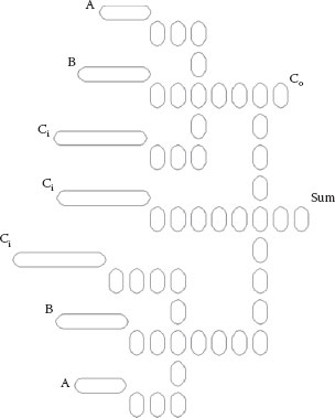
FIGURE 61.10 Schematic of the full adder including three three-input majority gates, and several high-aspect-ratio magnets to act as drivers providing the input data for the circuit. The majority gates are the intersections of horizontal and vertical wires at which the center magnet is influenced by three input magnets (top, left, and bottom neighbors) and influences an output magnet (right neighbor). (E. Varga et al., Implementation of a nanomagnetic full adder circuit, 11th International Conference on Nanotechnology (IEEE Nano), August 15–19, pp. 1244–1247, © (2011) IEEE. With permission.)
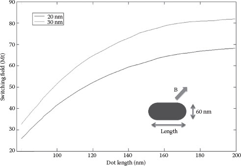
FIGURE 61.11 Simulated switching field versus dot (magnet) length. The thickness and width of nanomagnets are fixed. The monotonically increasing curvature suggests that the aspect ratio change can be exploited to design separately programmable inputs for the NML circuit.
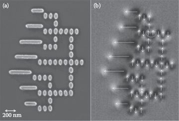
FIGURE 61.12 (a) SEM and (b) MFM images of a full adder constructed from 53 nanomagnets. Nearly perfect nanomagnet ordering is shown. Of the 53 magnets, only a single coupling failed (circled). (E. Varga et al., Implementation of a Nanomagnetic Full Adder Circuit, IEEE International Conference on Nanotechnology, Portland, OR, August 15–19, pp. 1244–1247, © (2011) IEEE. With permission.)
A homogeneous 200 mT field was applied first to set all the drivers pointing in the same direction, as shown in Figure 61.12b. Here, we do not magnetize the drivers separately; our goal is to test the operation of the entire structure for one set of input bits. The 200 mT magnetization was followed by a rotating field continuously decaying from 40 to 0 mT; this field demagnetizes the magnets to their computational ground state. More details about the choice of these field values are given in Ref. [4]. The MFM image (Figure 61.12b) shows a nearly perfect ordering of the nanomagnets, according to their neighbors, as required to correctly perform the logic operation. Of the 53 magnets, only a single coupling failed during the testing (at the output of the topmost majority gate—circled). This result is encouraging, as 52 of the 53 magnets fabricated in this complex geometry are correctly coupled to their neighbors, and all three majority gates functioned correctly. To the best of our knowledge, this circuit is the most complex NML circuit fabricated so far, and the first one that includes several logic gates. The error occurred at the circled position for three independent demagnetization events, suggesting that this error is most likely due to a design or fabrication error (an odd-shaped or pinned magnet). To achieve a truly error-free operation, the design and the fabrication parameters need to be optimized. There are several ways to design more compact NML full adders, as discussed below.
61.5 PROPOSED DESIGNS OF FULL ADDER
The tested full adder structure has a relatively high number of magnets, which increases the probability of errors during the switching process. One potential optimization process is to reduce the footprint of the structure and the number of magnets, as shown in Figure 61.13a. Here, there are 6 driver magnets and 25 small magnets. This design is already much smaller (altogether 31 magnets) than the previously tested one with 53 magnets (Figure 61.8).
The reduced footprint structures were fabricated successfully, as shown in Figure 61.13b. However, in this structure, the relatively long vertical and horizontal lines reveal a design flaw: the horizontal and vertical magnetic wires relax to their ground state at different external fields. This is due to the fact that for a horizontal applied field, the ferromagnetic coupling superposes to the applied field, so the horizontal (AFC) wires relax later than the vertical (FC) wires. This is why the magnet denoted with a star in Figure 61.11b fails to work correctly in 75% of the cases. An example is shown in Figure 61.14. The MFM image clearly displays two errors; the top one is the most common error for this layout.
OOMMF [16] simulations were performed to better understand the error formation mechanism. The results are summarized in Figure 61.15.
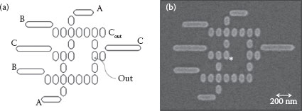
FIGURE 61.13 The reduced footprint NML full adder design. (a) Schematic and (b) SEM image of the Permalloy structure. The (*) symbol is explained in the text. (E. Varga et al., Implementation of a Nanomagnetic Full Adder Circuit, IEEE International Conference on Nanotechnology, Portland, OR, August 15–19, pp. 1244–1247, © (2011) IEEE. With permission.)
As the external field is decreased from the maximum value, the long horizontal wires start to switch to their antiferromagnetically ordered ground state at around the 60 mT field, while the vertical wires start to order at around 200 mT. This is a significant difference, and may cause the information to flow in the wrong direction. If a long horizontal wire precedes a long vertical wire segment in the signal flow, then the magnets of the vertical segment may fall into a random state before the effect of the drivers can reach them.
To avoid the above-mentioned issues coming from the different behaviors of the horizontal and vertical wires, we propose a new design (Figure 61.16). This design has a smaller footprint than any previous designs. The horizontal and vertical wires have decreased lengths, and the lengths of the driver magnets have been adjusted according to the simulation results shown in Figure 61.11.
The footprint can be reduced further by using asymmetric, slant magnets as inputs to the adder. The behavior of this magnet is summarized in Figure 61.8. As discussed above, the energy is not the highest when a device is magnetized along the horizontal direction, as is the case for the symmetric magnets (Figure 61.1). The design constructed from the slant and regular oval-shaped magnets is shown in Figure 61.17. The inputs are provided by the seven slant magnets, and the number of the rounded-edge magnets is only 14 (21 magnets altogether). The full adder has four different designs (Figures 61.17a through 61.17d) for testing all possible input combinations. Our goal is to demonstrate the correct operation of the gate for all logic cases. This can be completed by using fixed inputs, as shown in Figure 61.17 with slant input magnets.
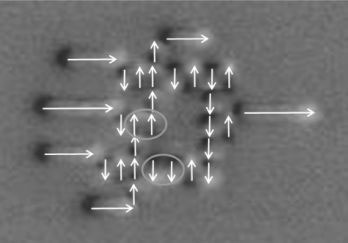
FIGURE 61.14 MFM image of the second full adder design (shown in Figure 61.13). Two errors (circled) are presented here; the top one is common and appears in 75% of the gates. (E. Varga et al., Implementation of a nanomagnetic full adder circuit, 11th International Conference on Nanotechnology (IEEE Nano), pp. 1244–1247, © (2011) IEEE. With permission.)
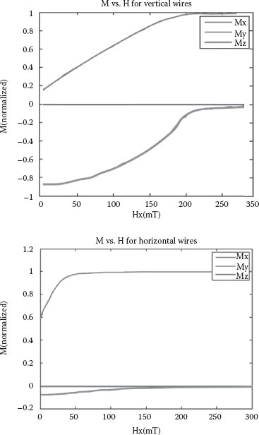
FIGURE 61.15 Simulation results for vertical (top) and horizontal (bottom) magnetic wires. The M versus H graph shows smooth switching behavior for the vertical line, though not for the horizontal one. Since the field is reduced from high to low values, the horizontal wire switches after the vertical wire. This difference has to be taken into account during the design of any NML structure. (E. Varga et al., Implementation of a nanomagnetic full adder circuit, 11th International Conference on Nanotechnology (IEEE Nano), pp. 1244–1247, © (2011) IEEE. With permission.)
In this chapter, we have presented the realization of complex NML circuits. A full adder design containing 53 magnets has been fabricated and tested with only one coupling error throughout the entire circuit. We concluded that these errors were most likely due to the fabrication and suboptimal design. It is challenging to design and fabricate high-yield NML circuits of such complexity. The low number of errors and the position of their occurrences suggest that improvement to no errors is possible.
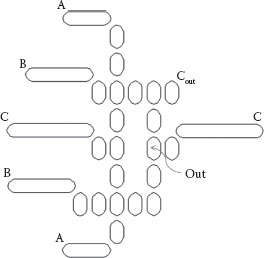
FIGURE 61.16 The proposed, new full adder design with decreased length of the magnetic wires.
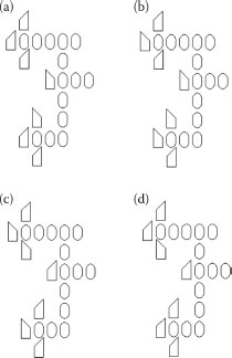
FIGURE 61.17 A reduced footprint design of the full adder. The inputs are provided by the slant magnets. Four different designs are shown (a through d) for testing all possible input combinations.
To realize complex functions in NML, one does not necessarily need to achieve a perfect ordering of large nanomagnet arrays. Large circuits can be split into smaller, individually clocked units, which then order and compute sequentially [17]. However, using large units significantly reduces the overhead of the clocking circuitry. With careful design and optimized technology, the realization of complex NML circuit units seems feasible.
1. A. Imre, G. Csaba, L. Ji, A. Orlov, G. H. Bernstein, and W. Porod, Majority logic gate for magnetic quantum-dot cellular automata, Science, 311(5758), 205–208, 2006.
2. E. Varga, M. T. Niemier, G. H. Bernstein, W. Porod, and X. S. Hu, Programmable nanomagnet-logic majority gate, IEEE Device Research Conference (DRC), Notre Dame, IN, Technical Digest, pp. 85–86, 2010.
3. E. Varga, M. T. Niemier, G.H. Bernstein, X. S. Hu, and W. Porod, Programmable nanomagnet-logic majority gate, IEEE DRC (Device Research Conference) Technical Digest, pp. 85–86, 2010.
4. E. Varga, A. Orlov, M. T. Niemier, X. S. Hu, G. H. Bernstein, and W. Porod, Experimental demonstration of fanout for nanomagnet logic, IEEE Transactions on Nanotechnology, 9(6), 668–670, 2010.
5. G. Csaba, W. Porod, and A. I. Csurgay, A computing architecture composed of field-coupled single domain nanomagnets clocked by magnetic field, International Journal of Circuit Theory and Applications, 31, 67–82, 2003.
6. M. Niemier, E. Varga, G. H. Bernstein, W. Porod, M. T. Alam, A. Dingler, A. Orlov, and X. Sharon Hu, Shape engineering for controlled switching with nanomagnet logic, IEEE Transactions on Nanotechnology, 11(2), 220–230, 2012.
7. E. Varga, S. Kurtz, M. T. Niemier, W. Porod, G. H. Bernstein, and X. S. Hu, Two input, non-majority magnetic logic gates: experimental demonstration and future prospects, Journal of Physics: Condensed Matter, 23(5), 053202, 2011.
8. E. Varga, M. Siddiq, M. T. Niemier, M. T. Alam, G. H. Bernstein, W. Porod, X. S. Hu, and A. Orlov, Experimental demonstration of non-majority, nanomagnet logic gates, IEEE DRC (Device Research Conference) Technical Digest, pp. 87–88, 2010.
9. E. Varga, M. T. Niemier, G. H. Bernstein, W. Porod, and X. S. Hu, Non-volatile and reprogrammable MQCA-based majority gates, IEEE DRC (Device Research Conference) Tech. Digest, pp 1–2, 2009.
10. P. D. Tougaw and C. S. Lent, Logical devices implemented using quantum cellular-automata, Journal of Applied Physics, 75(3), 1818–1825, 1994.
11. W. Wang, K. Walus, and G. A. Jullien, Quantum-dot cellular automata adders, 3rd IEEE Conference on Nanotechnology, 1–2, 461–464, 2003.
12. H. Cho and E. E. Swartzlander, Adder designs and analyses for quantum-dot cellular automata, IEEE Transactions on Nanotechnology, 6(3), 374–383, 2007.
13. K. Navi, S. Sayedsalehi, R. Farazkish, and M. R. Azghadi, Five-input majority gate, a new device for quantum-dot cellular automata, Journal of Computational and Theoretical Nanoscience, 7(8), 1546–1553, 2010.
14. E. Varga, G. Csaba, G. H. Bernstein, and W. Porod, Implementation of a nanomagnetic full adder circuit, 11th International Conference on Nanotechnology (IEEE Nano), August 15–19, pp. 1244–1247, 2011.
15. G. Csaba, M. Becherer, and W. Porod, Development of CAD tools for nanomagnetic logic devices, International Journal of Circuit Theory and Applications, Published online in Wiley Online Library (http://wileyonlinelibrary.com). DOI: 10.1002/cta.1811, 2012.
16. M. Donahue and D. Porter, OOMMF User’s Guide, Version 1.0, Interagency Report NISTIR 6367, http://math.nist.gov/oommf.
17. M. T. Alam, M. J. Siddiq, G. H. Bernstein, M. T. Niemier, W. Porod, and X. S. Hu, On-chip clocking for nanomagnet logic devices, IEEE Transactions on Nanotechnology, 9, 348–351, 2010.