0%
38Chapters
0-1Hours read
0kTotal Words
Book Description
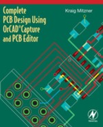
This book provides instruction on how to use the OrCAD design suite to design and manufacture printed circuit boards. The primary goal is to show the reader how to design a PCB using OrCAD Capture and OrCAD Editor. Capture is used to build the schematic diagram of the circuit, and Editor is used to design the circuit board so that it can be manufactured.
The book is written for both students and practicing engineers who need in-depth instruction on how to use the software, and who need background knowledge of the PCB design process.
- Beginning to end coverage of the printed circuit board design process. Information is presented in the exact order a circuit and PCB are designed
- Over 400 full color illustrations, including extensive use of screen shots from the software, allow readers to learn features of the product in the most realistic manner possible
- Straightforward, realistic examples present the how and why the designs work, providing a comprehensive toolset for understanding the OrCAD software
- Introduces and follows IEEE, IPC, and JEDEC industry standards for PCB design.
- Unique chapter on Design for Manufacture covers padstack and footprint design, and component placement, for the design of manufacturable PCB's
- FREE CD containing the OrCAD demo version and design files
Table of Contents
- Cover Image
- Table of Contents
- Copyright Page
- Introduction
- Acknowledgments
- Chapter 1. Introduction to PCB Design and CAD
- Chapter 2. Introduction to the PCB Design Flow by Example
- Chapter 3. Project Structures and the PCB Editor Tool Set
- Chapter 4. Introduction to Industry Standards
- Chapter 5. Introduction to Design for Manufacturing
- Chapter 6. PCB Design for Signal Integrity
- Chapter 7. Making and Editing Capture Parts
- Chapter 8. Making and Editing Footprints
- Chapter 9. PCB Design Examples
- Example 1. Dual Power Supply, Analog Design
- Example 2. Mixed Analog/Digital Design Using Split Power, Ground Planes
- Example 3. Multipage, Multipower, and Multiground Mixed A/D PCB Design With PSpice
- Example 4. High-speed Digital Design
- Chapter 10. Artwork Development and Board Fabrication
- Appendix A. List of Design Standards
- Appendix B. Partial List of Packages and Footprints and Some of the Footprints Included in OrCAD Layout
- Appendix C. Rise and Fall Times for Various Logic Families
- Appendix D. Drill and Screw Dimensions
- Appendix E. References by Subject
- Index
