Chapter 2. Introduction to the PCB Design Flow by Example
Now that we have covered the construction of a PCB and know PCB Editor’s role in it, we go through a simple design example so that you get a feel for the overall design process. This simple example sets the stage for Chapter 3, in which we dig deeper into the details of the process and learn more about PCB Editor itself and the PCB Design Examples.
Overview of the Design Flow
This section illustrates the basic procedure for generating a schematic in Capture and converting the schematic to a board design in PCB Editor. The basic procedure is as follows:
1. Start Capture and set up a PCB project using the PC Board wizard.
2. Make a circuit schematic using OrCAD Capture.
3. Use Capture to generate a PCB Editor netlist and automatically start PCB Editor and open the project as a .brd file.
4. Make a board outline.
5. Position the parts within the board outline.
6. Route the board.
7. Generate manufacturing data files.
Creating a Circuit Design with Capture
If you do not have a full version of OrCAD, you can go to the OrCAD Web site and download the latest demo. If you are using an older version of PCB Editor, most of the following information in this book still applies, but some of the dialog boxes and menu items may be different.
STARTING A NEW PROJECT
Before you make a PCB layout, you need to have a circuit to lay out. You use Capture to make the schematic, so the first step is to start the Capture application by clicking the Windows
Start button on your task bar and navigate to
All Programs→
OrCAD 16.0 Demo→
 . Once Capture is running, you should have a blank Capture session frame and a session log. Go to the
File dropdown menu and navigate to
File→
New and click
Project as shown in Figure 2-1.
. Once Capture is running, you should have a blank Capture session frame and a session log. Go to the
File dropdown menu and navigate to
File→
New and click
Project as shown in Figure 2-1.
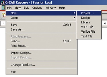 |
| Figure 2-1 Starting a new project in Capture. |
The
New Project dialog box in Figure 2-2 will pop up. Type a name for your project, then select the
PC Board Wizard radio button. If you feel comfortable selecting your own location to save the project, you can do that (use the
Browse… button), or you can use the default location for now (just remember where it is). Click
OK.
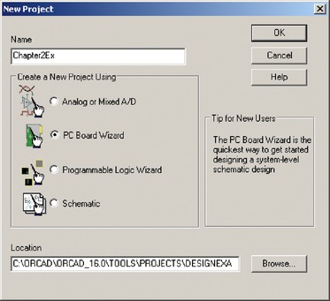 |
| Figure 2-2 New Project dialog box. |
After you click
OK, the PCB
Project Wizard dialog box shown in Figure 2-3 (left) will pop up. For now, circuit simulation will not be performed, so leave the
Enable project simulation box unchecked (we look at circuit simulation in the PCB Design Examples). Click
Next.
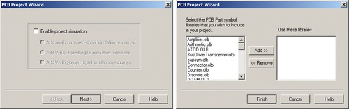 |
| Figure 2-3 PCB
Project Wizard dialog boxes: (left) simulation selection, (right) parts library selection. |
After you click
Next, the PCB
Project Wizard dialog box shown in Figure 2-3 (right) will pop up. This box allows you to add specific libraries to your project. Scroll down until you find the
Discrete.olb library, highlight it by clicking on it, then click the
Add>> button; then click
Finish. This completes the project setup.
You should have a
Project Manager window in the left side of the Capture session frame, as shown in Figure 2-4.
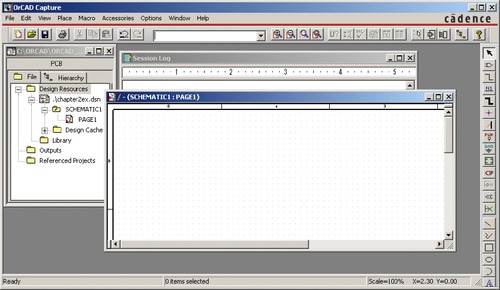 |
| Figure 2-4 Example view of a new project. |
You may also have a
Schematic window in the work space. If the schematic is not open, expand the
projectname.dsn directory by clicking the “ + ” box to the left of the
projectname.dsn icon (where
projectname is the name you gave your project while using the project setup wizard). Click the
+ box next to the
Schematics folder, then double click the file called
Page1. The Schematic page should open. If you do not see the dots, that means your grid is turned off.
The grid must be turned on to properly place and connect parts. To turn the grid on, click the Toggle Grid button,
 . If the grid is on, the grid dots are visible and the grid button is gray instead of red.
| Toggle Grid Button
|
Note: The menu bar at the top of the Capture session frame changes depending on whether you are working with the
Project Manager window or the
SchematicPage window. If you need to access options or tools for the Project Manager (or Schematic Page), you must have that window active. To make the desired window active, click on its title bar or select the desired window from the
Window menu. When inactive, it is gray; and when active, it is blue (or whatever colors you set up in
Windows). Also, for projects that have PSpice simulation capabilities, an additional toolbar is displayed, which is not shown in Figure 2-4.
PLACING PARTS
To add parts to your schematic, make the Schematic page active and select
Place from the
Part dropdown menu, or press the
Place Part tool button
 , or press
P on your keyboard. The
Place Part dialog box shown in Figure 2-5 will pop up. In the
Libraries selection box in the bottom left of the dialog box, click
DISCRETE. Then, in the
Part List box, click
R (for resistor). You should see its symbol in the preview window on the lower right. Click
OK. In the
Libraries window, you may have libraries different from that shown in Figure 2-5. At the very least, you should have the
DISCRETE library, since you had the wizard include it. If, for some reason, you do not see any parts or the
DISCRETE library is not there, you can follow along for now to get an overview of the process or you can find and add the library to your project.
, or press
P on your keyboard. The
Place Part dialog box shown in Figure 2-5 will pop up. In the
Libraries selection box in the bottom left of the dialog box, click
DISCRETE. Then, in the
Part List box, click
R (for resistor). You should see its symbol in the preview window on the lower right. Click
OK. In the
Libraries window, you may have libraries different from that shown in Figure 2-5. At the very least, you should have the
DISCRETE library, since you had the wizard include it. If, for some reason, you do not see any parts or the
DISCRETE library is not there, you can follow along for now to get an overview of the process or you can find and add the library to your project.
| Place Part tool button
|
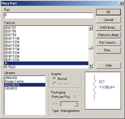 |
| Figure 2-5 Place Part dialog box. |
To add a part library to the project, select
Place from the
Part dropdown menu as described previously. In the
Place Part dialog box shown in Figure 2-5, press the
Add Library… button to bring up the
Browse File dialog box shown in Figure 2-6.
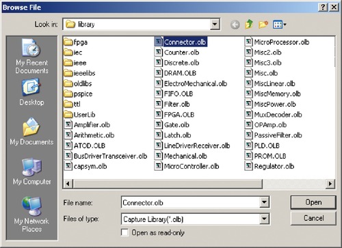 |
| Figure 2-6 Add a library using the
Browse File dialog box. |
Find and select the desired library and click
Open. You can also find a resistor in the
pspice library folder. To add it, double click the
pspice folder, select the
Analog.olb library, and click
Open. You should now be back to the
Place Part dialog box, and the library you just added should be shown in the
Libraries list box. Find and select
R from the
Part List selection box and click
OK.
After you click
OK, you should immediately return to the Schematic page and have a resistor tagging along with your mouse pointer. Left click on the schematic page to place the part as shown in Figure 2-7.
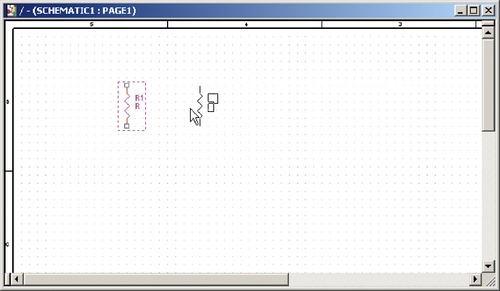 |
| Figure 2-7 Placing the parts. |
Place one resistor on the page; then hit the
ESC key or right click the mouse and select
End Mode from the pop-up menu. Before placing more parts, we assign a footprint to the existing part and make copies of it.
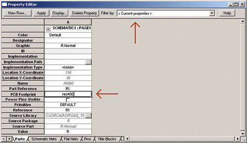
To assign a footprint to apart, double click the part to display the
Property Editor spreadsheet (see Figure 2-8). The cells may be shown vertically or horizontally. Find the
PCB Footprint cell and enter
res400. This is a basic through-hole, axial lead resistor footprint. Finding and selecting footprints is described in greater detail in Chapter 8. If the PCB Footprint variable is not shown, make sure that the
<Current properties> option is selected in the
Filter by: list. Once the footprint has been assigned, close the spreadsheet.
 |
| Figure 2-8 Assigning a footprint to a part with the Property Editor. |
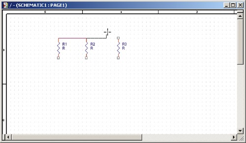
Next, duplicate the resistor. To do so, left click the resistor to select it and use standard Windows copy and paste procedures (
Ctrl + C and then
Ctrl + V, or
Edit → Copy and then
Edit → Paste from the menu) to place several copies of the resistor onto the schematic page.
WIRING (CONNECTING) THE PARTS
Next, connect the parts with wires.
To place wires, hit the
W key, select
Place → Wire from the
Place dropdown menu, or press the
Place Wire tool button,
 . The cursor will turn into a crosshair. Place the cursor on a box at the end of one of the resistor’s leads and left click to start a wire (see Figure 2-9).
| Place Wire tool button
|
 |
| Figure 2-9 Connecting the parts with wires. |
Click on the end of another resistor lead to complete that wire. The crosshair will persist, so you can continue placing wires. Finish connecting wires to the resistors however you wish. Once you have finished connecting the circuit, press the
ESC key or right click and select
End Wire to stop the place wire cursor and get the pointer back. If you inadvertently click near a lead but not on it, the wire may appear to be connected but may not be (that is why it is important to have the grid enabled). If the connections are not made properly, you will have problems when attempting to generate a netlist. You will be able to tell if a connection you made to a component was completed properly because the box at the end of the lead will disappear. At this point do not worry about power supplies or ground connections; this is just a “big picture” exercise to demonstrate the design flow process.
CREATING THE PCB EDITOR NETLIST IN CAPTURE
Once all the connections are complete, the next step is to create a netlist (a set of files that describes the circuit). Several types of netlists are possible, but you want
to generate a PCB Editor netlist. Begin by making the
Project Manager window active (instead of the
Schematic Page window) and select the
.dsn icon by left clicking it once. If the Schematic page is active, the
Tools menu will not be available. Minimize the Schematic page if necessary to get to the Project Manager. As shown in Figure 2-10, select
Tools → Create Netlist from the
Tools menu. The
Create Netlist dialog box will pop up as shown in Figure 2-10.
 |
| Figure 2-10 Creating a netlist for PCB Editor. |
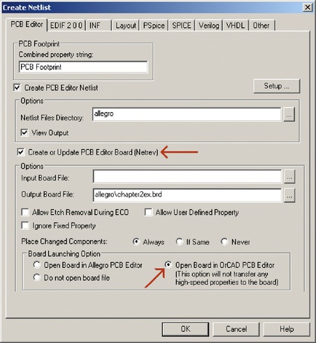
From the
Create Netlist dialog box, select the
PCB Editor tab. Select the
Create or Update PCB Editor Board (Netrev) option. For the time being, use the default output board file name and path. Select the
Create Open Board in OrCAD PCB Editor... option to automatically launch the PCB Editor applicaton. Click
OK to start the process.
Capture will display a warning text box stating
‘Directory “C:...projectnameallegro’ specified as Netlist directory does not exist. Do you want to create it? Click
Yes. Capture will display a warning text box stating
Design Path/projectname.dsn will be saved prior to netlisting. Click
OK.
You should then see the progress box shown in Figure 2-11 as the netlist is generated. Capture will then generate the netlist files, report the results in the Session log, and launch PCB Editor. If you had the
View Output option checked, the three netlist files will also be displayed in Capture. Leave Capture open so that it and PCB Editor can communicate with each other if necessary. This will allow you to go back and review the circuit if you need to when you are working in PCB Editor.
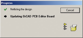 |
| Figure 2-11 The netlist
Progress dialog box. |
Designing the PCB with PCB Editor
The PCB Editor Window
Once the PCB Editor application is running, you should end up in the board layout environment shown in Figure 2-12.
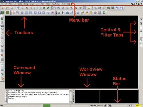 |
| Figure 2-12 The PCB Editor environment and initial view. |
Figure 2-12 shows six areas of the work environment. These areas are discussed in detail in Chapter 3 and only briefly introduced here. The design window is where you work on your board. With the design window and the various tools controlled by the control panel, menus, and toolbars, you can control various aspects of components, traces, and planes. Examples of controllable aspects include whether items are visible or not, whether they are fixed or movable, component location and orientation, and trace and board characteristics, to name just a few. The command window displays messages and prompts and allows you to enter commands. The worldview window gives you a bird’s-eye view of the location and size of the design widow relative to the actual PCB. The status window lets you know if the program is busy or idle and shows the coordinates of the crosshairs. The
P and
A buttons are related to the display and coordinates but are described later.
PCB editor begins with nothing in the design window and parts are not visible until they are placed, so we need to draw a board outline and place the parts.
CONTROLLING THE VIEW
The initial size of the design window is about 33 in. wide by 22 in. tall. To make a realistic board size for this simple example you want to zoom in. There are a couple of ways to do that. The zoom tools,
 , are Zoom to Points, Fit, In, Out, Previous, Selection, and Redraw, respectively. Click the Zoom to Points button,
 place the cursor at about coordinate position 4600, 3600 (units in mils, i.e., thousanths of an inch) then left click and release. Move the cursor down and to the left until it is less than or close to coordinates 0, 0. As the mouse is moved, a rectangular box with crossbars will become visible. Left click and release again to finish the Zoom to Points command. The design window covers a work area that is a little more than 4 in. by 3 in., which is plenty large for the few components in this example.
| Zoom tools
|
| Zoom to Points button
|
Drawing the Board Outline
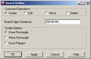
To draw the board outline, select
Setup → Outlines → Board Outline from the menu. The
Board Outline dialog box will be displayed, as shown in Figure 2-13. With the dialog box still displayed, move your mouse over to the design area and left mouse click at point 0, 0 (or close to it). While watching the cursor coordinates on the status bar (lower right side of the design window), move the mouse up about 4 in. (4000 mils) and to the right about 3 in. (3000 mils) and left click. A dashed outline will be displayed, and the
Board Outline dialog box changes to
Edit mode. The
Board Edge Clearance: determines how far from the edges of the board the place keep-in and route keep-in boundaries will be. The default value is 400 mils. For this design example, enter 200 mils in the text box and click
OK.
 |
| Figure 2-13 New
Board Outline dialog box. |
When you click
OK, another rectangle is automatically drawn inside the board outline. Actually there are two rectangles, one directly on top of the other. The two outlines are the route keep-in and package keep-in outlines. The route keep-in outline defines the edge of any plane layer and the boundary within which traces must stay. The package outline defines the area within which all components must reside.
If you hover your mouse over the inner rectangle, the data tips box will tell you which outline it is. You can turn that layer off to view the other rectangle. If the data tip says
Package/Keepin (or
Route Keepin), move your mouse over to the
Options tab (see Figure 2-14) to display the pane, and select
Package Keepin class from the list. Left click the colored box next to the
All subclass. The box will turn black and the place keep-in outline will disappear. You should then see the other outline, and the data tip should tell you it is the
Route Keepin/All outline (or the
Package Keepin). You can turn this one off by selecting
Route Keepin class from the
Options tab as described previously.
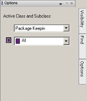 |
| Figure 2-14 The
Options pane. |
You can select and view the different boundaries by selecting them from the class list in the
Options pane or the
Visibility pane in the control panel area at the right of the design window (see Figure 2-14). The class and subclass for each outline so far is
Board Geometry & Outline,
Route Keepin and
All, and
Package Keepin and
All, respectively. Classes and subclasses are discussed in greater detail in Chapters 3 and 8 and the PCB Design Examples.
Placing Parts
Parts can be placed manually or automatically. Multiple automatic placement modes are available, but we wait until the PCB Design Examples to use them.
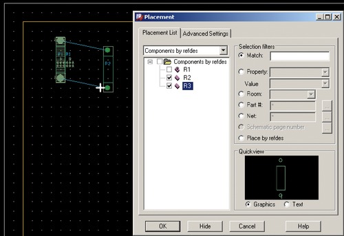
To place parts manually, select
Place → Manually… from the menu; click the
Manual Place button,
 , on the toolbar; or select
Place→
Manually… from the menu bar. The
Placement dialog box will be displayed, as shown in Figure 2-15. Select the
Placement List tab if it is not already selected. Click the
Components by refdes box; this will automatically select all the components. Leave the
Placement dialog box displayed (i.e., do not dismiss it by clicking the
OK or
Cancel button). Move the mouse cursor over to the design window; a component will be attached to it. Left click in the design window to place the part. The next part in the list will automatically be attached to the mouse cursor. The box next to the part that was just placed will be unchecked (it is no longer in the queue). Once all the parts are placed, dismiss the
Placement dialog box by clicking
OK
, on the toolbar; or select
Place→
Manually… from the menu bar. The
Placement dialog box will be displayed, as shown in Figure 2-15. Select the
Placement List tab if it is not already selected. Click the
Components by refdes box; this will automatically select all the components. Leave the
Placement dialog box displayed (i.e., do not dismiss it by clicking the
OK or
Cancel button). Move the mouse cursor over to the design window; a component will be attached to it. Left click in the design window to place the part. The next part in the list will automatically be attached to the mouse cursor. The box next to the part that was just placed will be unchecked (it is no longer in the queue). Once all the parts are placed, dismiss the
Placement dialog box by clicking
OK
.
| Manual Place button
|
 |
| Figure 2-15 Manually placing components. |
Moving and Rotating Parts
To move parts, select the
Move button,
 , click and release the left mouse button to select a part. Move the part to the desired location then click and release the left mouse button to place the part. You can continue moving other parts or right click and select
Done from the pop-up menu to deactivate the move tool.
To rotate a part, use the move tool as just described to select the part, then right click and select
Rotate from the pop-up menu. The component will pivot around pin 1 as you move the mouse around. Left click to stop rotating and left click again to place it, then right click and select
Done from the pop-up menu.
, click and release the left mouse button to select a part. Move the part to the desired location then click and release the left mouse button to place the part. You can continue moving other parts or right click and select
Done from the pop-up menu to deactivate the move tool.
To rotate a part, use the move tool as just described to select the part, then right click and select
Rotate from the pop-up menu. The component will pivot around pin 1 as you move the mouse around. Left click to stop rotating and left click again to place it, then right click and select
Done from the pop-up menu.
| Move button
|
Figure 2-16 shows the component footprints as well as the silk screen and assembly details. The parts of the footprint are
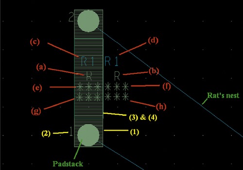 |
| Figure 2-16 Parts of a component footprint. |
Text:
a. Assembly top (Comp Value)
b. Silkscreen top (Comp Value)
c Assembly Top (Ref Des)
d. Silkscreen top (Ref Des)
e. Assembly top (Tolerance)
f. Silkscreen top (Tolerance)
g. Assembly top (User Part)
h. Silkscreen top (User Part)
Objects:
1. Place_Bound_Top (Package Geometry)
2. Pin_Number (Package Geometry)
3. Assembly_Top (Package Geometry)
4. Silkscreen_Top (Package Geometry)
You can change the visibility of the various parts of the footprint (and PCB as a whole) using the
Color and Visibility dialog box. Click the
Color button,
 , or select
Display → Color/Visibility from the menu.
To control the visibility of text objects, select
Components from the
Group list, as shown in Figure 2-17.
To control the visibility of package objects, select
Package Geometry from the
Group list as shown in Figure 2-18.
To control the visibility of padstacks, select
Stackup from the
Group list. You control the visibility of the various parts by checking or unchecking the boxes then clicking
Apply. You can customize the color of any text, etch, or detail object by selecting a color from the palate then clicking the color square of the item you want to customize. More will be said about footprint composition and construction in Chapter 8.
, or select
Display → Color/Visibility from the menu.
To control the visibility of text objects, select
Components from the
Group list, as shown in Figure 2-17.
To control the visibility of package objects, select
Package Geometry from the
Group list as shown in Figure 2-18.
To control the visibility of padstacks, select
Stackup from the
Group list. You control the visibility of the various parts by checking or unchecking the boxes then clicking
Apply. You can customize the color of any text, etch, or detail object by selecting a color from the palate then clicking the color square of the item you want to customize. More will be said about footprint composition and construction in Chapter 8.
| Color button
|
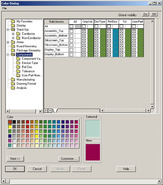 |
| Figure 2-17 Controlling the color and visibility of components objects. |
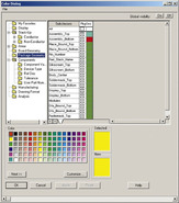 |
| Figure 2-18 Controlling the color and visibility of geometry objects. |
Routing the Board
USING THE AUTOROUTER
The next step is to route the board.
To route the board using the autorouter, select
Route → Route Automatic… from the menu; the
Automatic Router dialog box shown in Figure 2-19 will be displayed. The autorouter can be run in three modes. The different options will be demonstrated in the PCB Design Examples. For the time being, leave everything as is and click the
Route button.
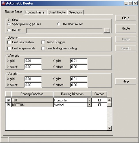 |
| Figure 2-19 Starting the autorouter. |
The autorouter will begin routing the board and a status box will be displayed (Figure 2-20). When the routing is complete the status box will be dismissed. Figure 2-21 shows how the board might look after routing.
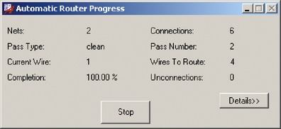 |
| Figure 2-20 Automatic Router Progress dialog box. |
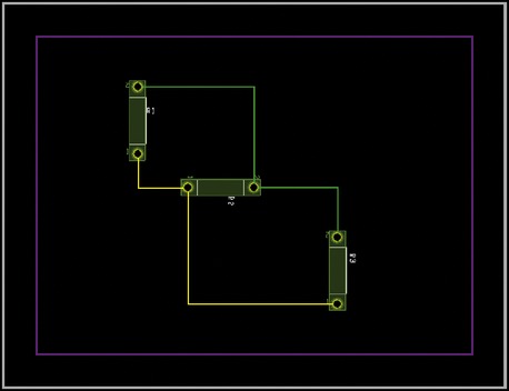 |
| Figure 2-21 Example of a routed board. |
In complex designs, you need to know how to use the manual routing tools to preroute critical traces and clean up after the autorouter. The manual routing tools are described next.
MANUAL ROUTING
In Chapter 3 and the PCB Design Examples, we take an extensive look at manually routing traces, so the manual routing is only briefly introduced here. First, unroute (rip up) the traces routed by the autorouter.
To rip up a trace, select the
Delete button,
 , and left click the trace you want to rip up. The trace will be highlighted. To complete the rip-up, click the trace again, select another trace, or right click and select
Done from the pop-up menu. Ripping up multiple (or all) traces from a list is demonstrated in the PCB Design Examples.
, and left click the trace you want to rip up. The trace will be highlighted. To complete the rip-up, click the trace again, select another trace, or right click and select
Done from the pop-up menu. Ripping up multiple (or all) traces from a list is demonstrated in the PCB Design Examples.
| Delete button
|
To begin manual routing, click the
Add Connect button,
 , on the toolbar. Left click a rat’s nest to begin routing. Left click again to place a vertex. Clicking on a pin ends the route, or you can right click and select
Finish to end the route. To stop routing, right click and select
Done from the pop-up menu.
, on the toolbar. Left click a rat’s nest to begin routing. Left click again to place a vertex. Clicking on a pin ends the route, or you can right click and select
Finish to end the route. To stop routing, right click and select
Done from the pop-up menu.
| Add Connect button
|
Note: If the route tool does not seem to be working, display the
Find pane and make sure that
Ratsnest box is checked.
To add a via, select a net with the
Add Connect tool, place a vertex, right click, and select
Add Via from the pop-up menu. A via will be placed at the vertex and routing continues on the alternate layer listed in the
Options pane.
If you want
to push (move) a trace without rerouting it, use the
Slide button,
 . Left click the trace, move your mouse pointer to the desired location, and left click again to place the trace.
| Slide button
|
By using the control panel’s
Options pane, you can change routing properties, such as the active layer (
Act), alternate layer (
Alt), the trace width, and line type.
To select a different routing layer, use the
Act dropdown list to select the desired layer. When you are finished routing, right click and select
Done from the pop-up menu.
These are just a few of the basic tools you need to know about. In the PCB Design Examples, you will see how to use more of the tools and control routing properties, such as setting minimum and maximum trace widths and setting up plane layers.
PERFORMING A DESIGN RULE CHECK
After you have completed routing your board, you should check for errors.
To check for errors, run the design rule checker (DRC) by selecting
Tools → UpdateDRC from the menu. A message will be displayed in the console window (at the bottom of the screen) as to whether there were errors. If there are errors, the message in the console window does not go into detail about what they are, just that they exist. If you want to see a description of the errors, run a DRC report.
To run a DRC report, select
Tools → Quick Reports → Design Rules Check Report from the menu. An example of a DRC Report is shown in Figure 2-22. The report shows what would be reported if R2 and R3 were too close to each other (not the circuit in Figure 2-21).
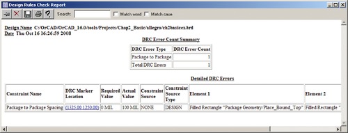 |
| Figure 2-22 An example DRC report. |
Creating Artwork for Manufacturing
At this stage, PCB Editor has generated a design file that fully describes your board. This file is optimized for viewing, editing, and saving on your computer, but it is not in the format that many PCB manufacturers use for fabricating boards. The most common type of file system used in PCB manufacturing is the Gerber file system. PCB Editor has the capability of translating its .brd file to Gerber files. In PCB Editor, this is called
manufacturing the design. PCB Editor allows considerable control over the manufacturing. As a result, several steps are required to generate all of the manufacturing files, especially with more complicated designs. Setting up the manufacturing process and generating the Gerber files is described in detail in Chapter 10. A quick overview is given here.
To create artwork for your design, select
Manufacture → Artwork… from the menu or click the
Artwork button,
 , on the toolbar. The
Artwork Control Form shown in Figure 2-23 is used to create the artwork. Artwork files and NC drill and router file creation are described in detail in Chapter 10.
, on the toolbar. The
Artwork Control Form shown in Figure 2-23 is used to create the artwork. Artwork files and NC drill and router file creation are described in detail in Chapter 10.
| Artwork button
|
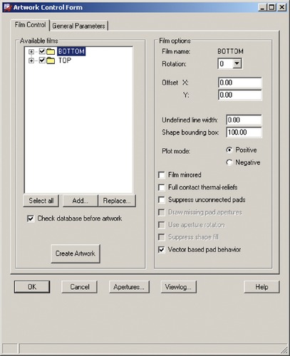 |
| Figure 2-23 Artwork Control Form dialog box. |
Congratulations, you have routed your first PCB using OrCAD PCB Editor! The objectives of this chapter were to demonstrate the basic steps of designing a circuit schematic and using PCB Editor to design a PCB. The following is a summary of the process:
1. Start Capture and set up a PCB project using the PC Board wizard.
2. Make a circuit schematic using OrCAD Capture.
3. Use Capture to generate a PCB Editor netlist and automatically start PCB Editor.
4. Make a board outline.
5. Position the parts within the board outline.
6. Route the board.
7. Generate manufacturing artwork.
In the next chapter, we cover the design flow in greater detail and learn more about the PCB Editor tool set; and in Chapters 8 and 9 and the PCB Design Examples, we learn more about footprint design, PCB layer design, and the steps to manufacturing the board design.
..................Content has been hidden....................
You can't read the all page of ebook, please click here login for view all page.