This example shows how to design a circuit with a mixture of analog and digital parts, multiple power planes, and a single Ground plane split into analog and digital sections that have a common reference point.
Mixed-Signal Circuit Design in Capture
Figure 9-90
shows the circuit design example. The circuit consists of a mixture of analog and digital parts, multiple power sources, and separate analog/digital Ground planes. It has an off-board connector, an analog signal conditioning circuit (the op amp U1), an analog-to-digital converter (U2), a digital microcontroller (U3), and a digital serial-to-parallel shift register (U4). Note that the bypass capacitors have been omitted to accommodate the part count limitations of the demo version of the software.
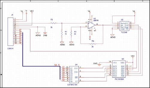 |
| Figure 9-90 Mixed-signal schematic design in Capture. |
The circuit has five global power nets, which include analog power (V+, V−) and analog ground (AGND) for U1 and U2, and 5-V digital power (VCC) and digital ground (GND) for U3 and U4. Analog and digital grounds are often kept separate to help prevent digital switching noise from affecting the analog ground. But, for the circuit to work (especially when using analog-to-digital and digital-to-analog converters), the two grounds must have a common reference point. The two grounds are tied together through a low-impedance, single-point connection at the connector.
The procedures and tools described in the first example are used to start a new project; place the parts onto the schematic page, connect the parts, and assign footprints.
Table 9-4
lists the parts used and the footprint assignments. The conn14 footprint symbol is a modified version of the one included with the software (it is not included with the demo version); a copy of the modified symbol is included on the Web site that accompanies this book.
There are a couple of significant differences between this and the last example. The differences include
1. All analog parts and some digital parts have explicit connections to power and ground nets, while the shift register is connected to the digital power and ground globally, as described later.
2. Two different ground symbols (CAPSYMs) are connected to one net.
3. Some of the connections are made with a bus rather than wires.
POWER AND GROUND CONNECTIONS TO DIGITAL AND ANALOG PARTS
Digital gates from the Capture libraries have nonvisible (invisible) power and ground pins. Their power pins are named
VCC and their ground pins are named
GND. Connecting a wire to an invisible power pin does nothing. Connections from nets to invisible power pins can be made only through global net names (made global by CAPSYM power, ground symbols, or off-page connectors). So the power pin VCC on U4 (CD74HC164) is connected to the schematic’s VCC symbol by the name
VCC and the ground pin is connected to the digital ground symbol by the name
GND.
To connect a digital gate’s ground pin to a ground net in your schematic, you have to either name the digital ground net
GND or change the name of the digital gate’s ground pin to match the name you assigned to the digital ground net (e.g.,
DGND instead of
GND)—this is required for all digital gates. It is easiest to use the default
GND name for the digital ground.
Most other Capture parts use either visible power pins or input or passive pins for power and ground. And instead of using
VCC and
GND as names of the power pins, they often use
V+ and
V− or
VDD and
VSS. When parts use visible power and ground pins, you can either take advantage of their global nature (and simply use their names to make connections to global nets) or make direct connections to the pins with wires. When parts use input or passive pins for power and ground, you have to make explicit connections (using wires) between the pins and the power or ground nets. Said another way, you cannot make connections to invisible power pins, and you have to make connections to pins that are not power pins; but visible power pins may have either wired or global connections to them. When you make an explicit connection to a visible power pin with a wire, the pin becomes connected to that net (the name of the wire) regardless of the name of the pin.
CONNECTING SEPARATE ANALOG AND DIGITAL GROUNDS TO A SPLIT PLANE
The CAPSYM power and ground symbols are global in nature and share characteristics of nonvisible power pins (i.e., connections to nets can be made by name or by physical connections).
Figure 9-91
shows how the analog and digital grounds are named and displayed. Two CAPSYM symbols are used with distinct names to differentiate the two ground systems. The analog parts of the circuit are referenced to the analog ground (AGND) symbol and the digital components are referenced to the digital ground (GND) symbol. At some point the two grounds need to be connected together for the analog-to-digital converter to work correctly (particularly with single-ended inputs). At the connector the two grounds may leave the board separately and be connected at the power supply, or they may be connected at a pin (or pins) and leave the board together as one common ground. In this example the two grounds are connected at pin 5.
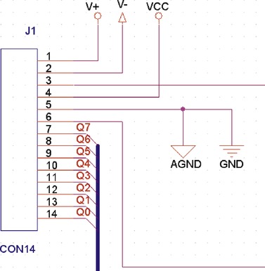 |
| Figure 9-91 Connection of the analog and digital grounds and bus connections. |
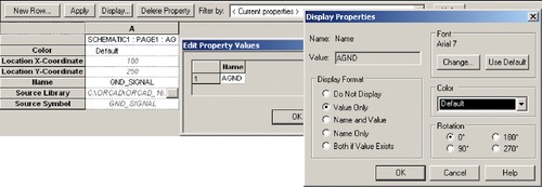
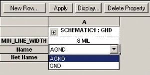
To place the analog and digital ground symbols, use the Place Ground tool,
 , and select the desired ground symbols. To change the symbol’s name, select the ground symbol (for example, from
GND_SIGNAL to AGND), select the symbol on the schematic page to highlight it, right click, and select
Properties from the pop-up menu to display the
Properties spreadsheet (see
Figure 9-92
). Select the
Name row, right click, and select
Edit from the pop-up menu to display the
Edit Property Values dialog box. Enter the new name of the ground symbol and click
OK. To display the name of the symbol on the schematic page, click the
Display button on the top of the spreadsheet and select the appropriate radio button on the
Display Properties dialog box (
Figure 9-92
).
, and select the desired ground symbols. To change the symbol’s name, select the ground symbol (for example, from
GND_SIGNAL to AGND), select the symbol on the schematic page to highlight it, right click, and select
Properties from the pop-up menu to display the
Properties spreadsheet (see
Figure 9-92
). Select the
Name row, right click, and select
Edit from the pop-up menu to display the
Edit Property Values dialog box. Enter the new name of the ground symbol and click
OK. To display the name of the symbol on the schematic page, click the
Display button on the top of the spreadsheet and select the appropriate radio button on the
Display Properties dialog box (
Figure 9-92
).
| Place Ground tool
|
 |
| Figure 9-92 Changing a ground/power symbol’s name and displaying it. |
Place the second ground symbol and rename it (if applicable). Use the Wire tool to connect the two ground symbols together then to the connector pin. The two ground symbols were distinct global nets until they were connected by the wire (net). Nets typically have names such as N04432 unless they are connected to a global net or symbol, then they take on the global name. A net can have only one name, and since the net just placed is connected to two global symbols with different names, it has to pick one of them (it decides alphabetically).
To select the name of a global net, double click the net (or select the net and right click and select
Properties) to display the
Schematic Net Properties spreadsheet (
Figure 9-93
), select the
Name row, right click, and select
Edit to display the
Edit Property Values dialog box. Use the dropdown selection list to choose which name the net should go by. Click
OK and then close the spreadsheet.
 |
| Figure 9-93 Selecting the ground net name. |
It appears on the schematic that the analog and digital grounds are separate ground systems, connected only at J1. As far as Capture is concerned, they are actually the same net—the name of which was decided in the dropdown list in
Figure 9-93
. Once we get to PCB Editor, we will separate the ground systems using a split plane.
USING BUSES FOR DIGITAL NETS
Digital circuits often have multiple, related input/output wires. The serial-to-parallel shift register in
Figure 9-90
is an example, in which Q0 through Q7 are data lines that represent the analog voltage sampled by the analog-to-digital converter as an 8-bit word. Rather than draw all eight lines throughout your schematic, you can group the eight members of the word into a single bus (the blue line in
Figure 9-90
and
Figure 9-91
).
A bus is a solid line that represents a group of wires or signals. Buses are not used to make connections to pins, but buses contain the signals connected to pins. Signal lines are added to a bus through aliases. Nets that are contained in buses are named, for example, A0, A1, A2, and A3, and the bus that contains them is named A[0..3].
Buses are placed on the schematic using the Place Bus tool,
 [
Bus_Button]. After you have placed the bus, you define (name) it with an alias using the Place Net Alias tool,
[
Bus_Button]. After you have placed the bus, you define (name) it with an alias using the Place Net Alias tool,
 . Buses are named by a specific convention,
busname[n..m], in which
busname is the alias (a name you give it) and [
n..m] is a member list made up of integers. The integer
n in
busname[n..m] is the first member of the list and integer
m is the last member of the bus list. The integers within the list can be separated with two periods,
[n..m]; a colon,
[n:m]; or a dash,
[n–m]. The nets (wires) that make up the members are placed on the schematic using the Place Wire tool,
. Buses are named by a specific convention,
busname[n..m], in which
busname is the alias (a name you give it) and [
n..m] is a member list made up of integers. The integer
n in
busname[n..m] is the first member of the list and integer
m is the last member of the bus list. The integers within the list can be separated with two periods,
[n..m]; a colon,
[n:m]; or a dash,
[n–m]. The nets (wires) that make up the members are placed on the schematic using the Place Wire tool,
 . The bus members are placed on the schematic as you would place any other wire, but they are added to the bus by giving the wire a name (a member alias) that associates it with the bus. The members are named as
busnamen through
busnamem with the Place Net Alias tool. So in this example, the bus alias is named
Q[0..7], and the member aliases are named
Q0,
Q1, to
Q7. The short, slanted lines that are used to connect the wires to the bus are placed on the schematic using the Place Bus Entry tool,
. The bus members are placed on the schematic as you would place any other wire, but they are added to the bus by giving the wire a name (a member alias) that associates it with the bus. The members are named as
busnamen through
busnamem with the Place Net Alias tool. So in this example, the bus alias is named
Q[0..7], and the member aliases are named
Q0,
Q1, to
Q7. The short, slanted lines that are used to connect the wires to the bus are placed on the schematic using the Place Bus Entry tool,
 . Or you can
add slanted lines yourself: Select the Place Wire tool, hold down the
Shift key on your keyboard, left click to start the wire, release the
Shift key, and left click to end the wire.
. Or you can
add slanted lines yourself: Select the Place Wire tool, hold down the
Shift key on your keyboard, left click to start the wire, release the
Shift key, and left click to end the wire.
| Bus_Button tool
|
| Net Alias tool
|
| Place Wire tool
|
| Place Bus Entry tool
|
The microcontroller (U3) has a couple of unused pins. To indicate that the pin is a “no-connect,” place a no-connect symbol on the pins by selecting the
Place no connect button,
 , from the toolbar and place no-connect symbols on the unused pins.
| Place No Connect button
|
Note: Any pin in a schematic used to make a PCB can have a no-connect symbol, but when PSpice simulations are performed, some pins are not allowed to “float” and the no-connect symbol cannot be used. In that case enter
RtoGND in the
FLOAT property in the
Properties spreadsheet. For more information see the
Capture User Guide, cap_ug.pdf, and search for RtoGND.
Once the design is completed, it is a good idea to do some housecleaning and design checking before making the netlist. Such tasks (as described in the previous example) include
1. Perform an annotation to clean up part numbering.
2. Make sure that global power/ground nets are properly named.
3. Make sure all parts have the correct footprints assigned to them (use the BOM to assist).
4. Perform a DRC to verify that the circuit design has no issues.
5. Correct any errors and reperform the DRC as needed.
Once the design has been second-checked and is free of errors, create the PCB Editor netlist as described in the first example (from the Project Manager go to
Tools → Create Netlist and select the PCB Editor tab).
..................Content has been hidden....................
You can't read the all page of ebook, please click here login for view all page.