23
Delta sigma ADC bridge measurement techniques
Introduction
Sensors for pressure, load, temperature, acceleration and many other physical quantities often take the form of a Wheatstone bridge. These sensors can be extremely linear and stable over time and temperature. However, most things in nature are only linear if you don’t bend them too much. In the case of a load cell, Hooke’s law states that the strain in a material is proportional to the applied stress—as long as the stress is nowhere near the material’s yield point (the “point of no return” where the material is permanently deformed). The consequence is that a load cell based on a resistance strain gauge will have a very small electrical output—often only a few millivolts. In spite of this, instruments with 100,000 counts of resolution and more are possible. This Application Note presents some new approaches to high resolution measurement made possible by Linear Technology’s family of 20- and 24-bit delta-sigma analog-to-digital converters.
Often the biggest hurdle in implementing a 20- or 24-bit bridge measurement circuit is moving beyond the conventional signal conditioning circuitry required for 12- to 16-bit ADCs. Simply substituting a 24-bit ADC in a circuit designed for a 12-bit ADC does not guarantee a 4096 fold increase in resolution. While performance may be improved, the 24-bit ADC may simply reveal the limitations of the analog front-end, and the full benefit of the 24-bit ADC will not be realized.
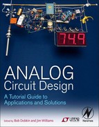
In a typical 12-bit measurement system, the signal conditioning amplifier requires a very high gain in order to make use of the full ADC input range. A sensor with a 10mV full-scale output requires a gain of 500 to use the full input range of a typical 5V input ADC. A filter may be required to reduce noise at the expense of settling time. Additional difficulties arise when dealing with the large common mode voltage typical of a bridge sensor. Most instrumentation amplifiers have a large discrepancy between the typical CMRR and guaranteed minimum, which may require an additional trim.
Linear Technology’s differential input delta sigma ADCs address these concerns and make it possible to extract maximum resolution from a variety of bridge measurement devices. The outstanding resolution of these ADCs eliminates the need for amplification in many applications. Even in extreme cases where amplification is required, high resolution ADCs such as the LTC®2440 allow very modest amplifier gains. A fully differential amplifier topology eliminates the differential-to-single-ended stage of a typical
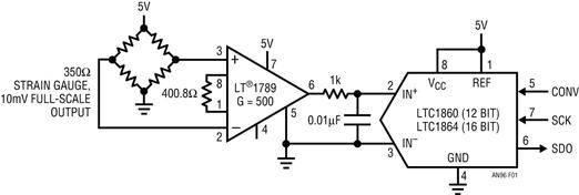
Figure 23.1 Typical 12-Bit to 16-Bit System
3-amplifier instrumentation amplifier along with the CMRR limitations of this stage.
Linear Technology’s delta sigma ADCs also simplify noise filtering. The internal SINC4 FIR digital filter results in a very small noise bandwidth (6Hz at 7.5 samples/second) without the long settling time associated with an analog filter of equivalent bandwidth. Thus no filter is required to prevent an amplifier’s noise from reducing resolution, or to reject 50Hz-60Hz line pickup.
The 120dB minimum CMRR of the ADC itself eliminates concern about the mid-supply common mode voltage of a typical bridge sensor. The ADC also lends itself readily to floating measurements with little additional circuitry. See Design Note 341.
Understanding the capability of the sensor is a critical aspect of measurement circuit design. Often a requirement is stated as a number of “bits of resolution” without taking into account the sensor’s limitations, or even the sensor’s output voltage. Lack of familiarity with the sensor can result in an improperly designed circuit (bad for product performance) or an overdesigned circuit (bad for financial performance). The applications that follow are developed starting at the sensor and considering its performance in terms of physical units; i.e., kgs, PSI, etc., disregarding the number of “bits” as a figure of merit until the conclusion.
Low cost, precision altimeter uses direct digitization
The availability of small, low cost, piezoresistive barometric pressure sensors has led to a plethora of portable devices with barometer and altimeter functions. The LTC2411 is a perfect companion to these sensors, as it is capable of outstanding resolution with no analog signal conditioning at all.
The NPP301-100 absolute pressure sensor from G.E. Lucas Novasensor is a piezoresistive device in an SO-8 package. Full-scale output is 20mV per volt of excitation voltage at one atmosphere (the sensor’s full-scale input). Temperature coefficient of span is nominally −0.2%/°C (typical of piezoresistive sensors) and the temperature coefficient of offset is ±0.04%/°C.
The formula for altitude vs pressure, based on the 1976 U.S. standard atmosphere is:
where P is the pressure at a given altitude and P0 is the pressure at sea level.
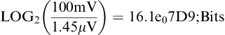
The input resolution of the LTC2411 is 1.45μVRMS (independent of reference voltage), providing a pressure resolution of:
![]()
(0.00043 inches of mercury)
when the bridge is excited with 5V. 0.0145mB corresponds to an altitude resolution of 5 inches at sea level, everything else being perfect.
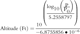
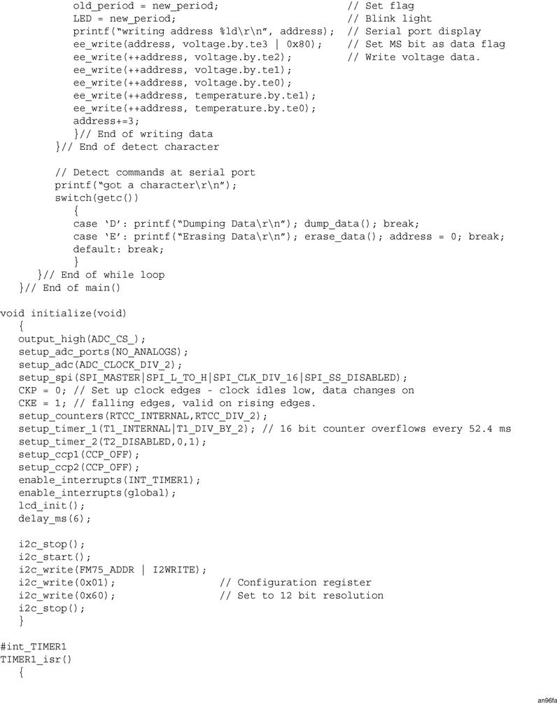
The circuit shown in Figure 23.2 records pressure and temperature data once every 15 seconds to a 32k EEPROM. An FM75 pre-calibrated temperature sensor measures temperature. Each data point contains the entire 32-bit output word from the LTC2411 and temperature to the nearest 1/16°C. Three AA cells provide both power and a quiet reference voltage. The ratiometric bridge measurement cancels the effect of long-term drift of the battery voltage. The overall accuracy of the measurement is not affected by reduced battery voltage, however the noise floor increases proportionally.
Figure 23.2 Logging Altimeter
Figure 23.3 shows altitude data from a steep hike to the top of Mission Peak (summit at 767m (2517ft) in Fremont, CA) on a cold evening. The raw altitude data clearly shows the barometric sensor’s temperature sensitivity—the indicated altitude at the summit is more than 152m (500ft) too low due to the drop in temperature. Correcting for temperature effects based on the nominal −1900ppm/°C bridge temperature coefficient brings the maximum altitude to 780m (2560ft), much closer to the true value of 767m (2517ft). More accurate results are possible with further calibration.

Figure 23.3 Example Altitude Data
How Many Bits?
The effective number of bits based on the ADC resolution and 100mV output of the sensor is
The Marketing department will raise their eyebrows and devote whole ad campaigns around the extra 0.1 bit and five inch resolution. A skydiver or mountaineer, though, is more concerned with the overall absolute accuracy in a wide range of conditions than the impressive sounding number of bits.
Increasing Resolution with Amplifiers
Linear Technology’s delta sigma ADCs eliminate the need for instrumentation amplifiers in many instances. However, if the ADC by itself is not adequate, a properly designed amplifier can increase the overall resolution.
Figure 23.4 shows a differential amplifier with an input resolution of 375nVRMS over the bandwidth of the LTC2431. The LTC2051 is an autozero amplifier with an input offset of 3μV and an offset drift of 30nV/°C, ideal for applications in which long-term drift and accuracy are critical.

Figure 23.4 Low Noise Differential Amplifier
How Much Gain?
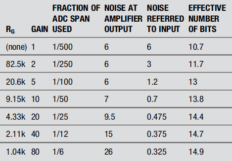
With high resolution ADCs, it is often unnecessary (and sometimes detrimental) to match the amplifier’s output range to the input range of the ADC. Instead, limit the gain to a value such that that the overall resolution is limited by the amplifier’s input noise.
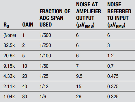
Table 23.1 shows the effects of various gains on the performance of the circuit in Figure 23.4. At a gain of 1, the 5.6μVRMS input noise of the LTC2431 ADC dominates. At a gain of 2, the noise of the ADC still dominates, but the input resolution is doubled. Around a gain of 30, the amplifier’s input noise starts to dominate. Increasing gain to more than 40 only provides an incremental improvement in resolution. Increasing the gain further increases the measurement errors due to the LTC2051’s bias current and finite open-loop gain. Even at a gain of 80, less than 20% of the ADC’s input range is used if the input is a standard 10mV output strain gauge. Don’t be tempted to bump the gain to 250 to use the whole ±2.5V input range; the overall resolution will not be improved.
Table 23.1
ADC Response to Amplifier Noise
When properly designed, the resolution of this circuit is limited almost entirely by the amplifier’s input noise. This is the case whenever the amplifier’s input noise is lower than the ADC’s input noise (there is no point in using an amplifier that is noisier than the ADC). So how does one determine the total noise from the ADC and amplifier data sheets?
This is an easy exercise with low resolution sampling converters. The ADC inputs typically have a flat frequency response out to the full-power bandwidth given in the data sheet (which may be significantly higher than 1/2 of the ADC’s maximum sample rate). The bandwidth of the amplifier-ADC combination is limited by either the amplifier’s bandwidth or the ADC’s full-power bandwidth. As long as the total noise that gets through this system (calculated from the amplifier’s wideband noise and the square root of the smaller of the amplifier bandwidth or the ADC bandwidth) is a small fraction of an LSB, the problem is solved. Common noise reduction techniques are simple RC filters directly in front of the ADC or a 2nd order Sallen-Key filter.
Once again, Linear Technology’s delta sigma ADCs change the approach to noise reduction. The full-power bandwidth of these devices is approximately 3Hz when operating in the 50Hz or 60Hz rejection mode (7.5sps or 6.25sps) and the response to wideband noise is equivalent to a 6Hz brickwall filter. It is exceedingly difficult to build an analog filter that will improve upon this without degrading some other parameter.
The 6Hz bandwidth figure predicts total noise fairly accurately for autozero amplifiers that have flat noise power densities from DC to some frequency higher than 6Hz. (Note that this bandwidth must be scaled appropriately if the conversion rate is changed by applying an external conversion clock. For instance, applying a 300.7kHz conversion clock to an LTC2411 will result in a 12Hz noise bandwidth.)
For most amplifiers, a good first estimate of the ΔΣ ADC’s response to amplifier noise is the 0.1Hz to 10Hz peak-to-peak noise specification divided by a crest factor of six. 1It is only fair to calculate noise from 10 seconds worth of ADC data for non-autozero amplifiers; longer sets of data contain 1/f noise components below 0.1Hz as well as thermal drift components.
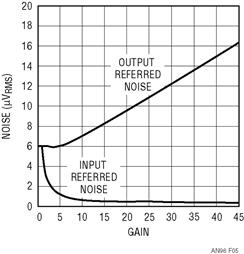
Figure 23.5 Noise vs Gain
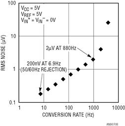
Figure 23.6 LTC2440 Speed vs RMS Noise
The 0.1Hz to 10Hz noise for the LTC2051HV is 1.5μVP-P or 1.5μV/6 = 250nVRMS. Since two amplifiers are used, the total noise is 250nVRMS • ![]() = 353nVRMS, very close to the measured value. (This rule has proved fairly accurate in a large number of experiments with both autozero and low-noise bipolar amplifiers.)
= 353nVRMS, very close to the measured value. (This rule has proved fairly accurate in a large number of experiments with both autozero and low-noise bipolar amplifiers.)
How Many Bits?
Table 23.2 extends Table 23.1 with another column for the effective number of bits based on the input-referred noise and a 10mV full-scale input signal at 7.5 sample/sec.
Table 23.2
Faster or More Resolution with the LTC2440
The LTC2440 has an input noise of 200nVRMS at the base data output rate of 6.8sps—seven times lower than the LTC2411. Also, the variable oversample ratio allows speed and resolution to be optimized for a given application.
Decreasing the oversample ratio by a factor of 2 increases the data rate and effective bandwidth by a factor of 2, the total noise increases by a factor of ![]() , and the effective number of bits is reduced by 1/2 bit. (Increasing data rate by 4 reduces ENOB by 1 bit.) This relationship holds for data output rates from 6.8Hz to 880Hz. The highest two output rates include additional quantization noise, but the linearity, offset, and full-scale error do not change.
, and the effective number of bits is reduced by 1/2 bit. (Increasing data rate by 4 reduces ENOB by 1 bit.) This relationship holds for data output rates from 6.8Hz to 880Hz. The highest two output rates include additional quantization noise, but the linearity, offset, and full-scale error do not change.
This increase in performance does not come entirely for free. The LTC2411 family devices are relatively easy to drive. Source impedances of up to 10k do not degrade performance if parasitic capacitance at the inputs is kept to a minimum, and the effective input impedance is on the order of 3MΩ to 5MΩ. On the other hand, the LTC2440 samples the inputs at 1.8Msps, or 11.5 times faster than the LTC2411. This means that any disturbance at the inputs must settle more than 11.5 times faster and the effective input impedance is approximately 110kΩ. There are two ways to meet the settling time requirement: lower the source impedance or keep any sampling disturbance from happening at all. Resistive sources located very close to the LTC2440 can meet these criteria; current shunts and 350Ω strain gauges may not require any signal conditioning at all. Most signals, though, require buffering of some sort. The LTC2440 data sheet contains a further discussion of these effects.
Sampling glitches from the LTC2440 contain very high frequency components (>250MHz). Loading the inputs to the LTC2440 with large (1μF) capacitors reduces the sampling glitches to an insignificant level. Of course, most amplifiers do not behave very well when driving this sort of load, so additional compensation is required.
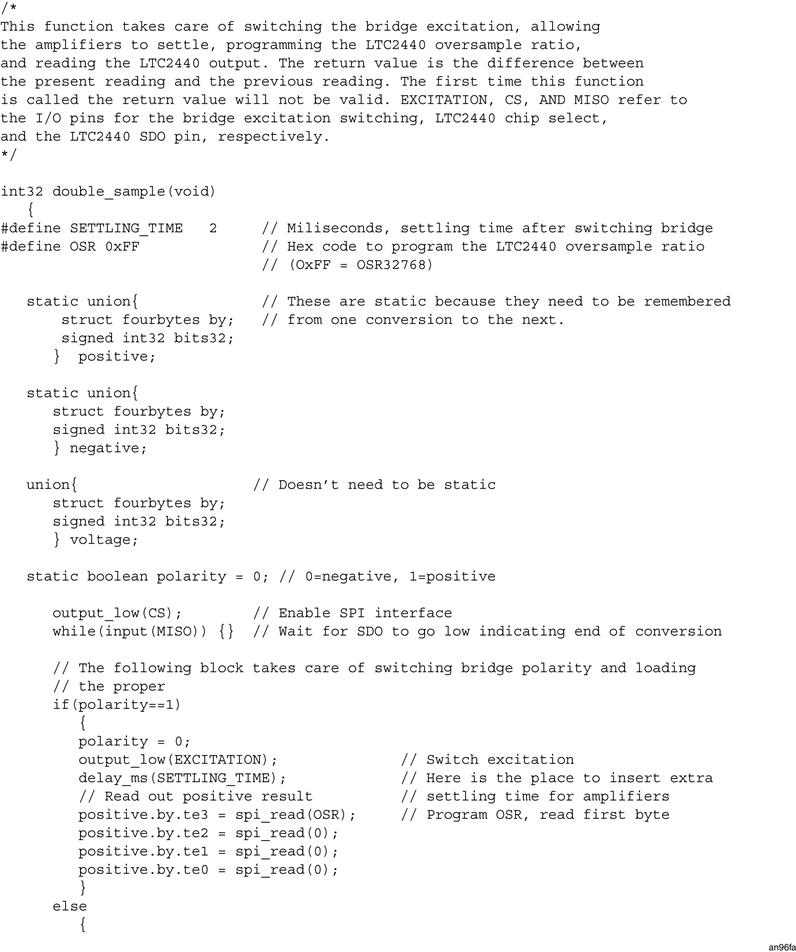
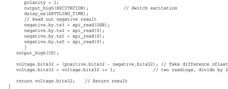
Figure 23.7 shows a basic high impedance buffer for applications that require DC accuracy. During a conversion, the disturbances emanating from the ADC’s inputs are attenuated by the ratio of CSAMPLE/1μF, or ∼100dB for the LTC2440, and the amplifier simply supplies the average sampling current.
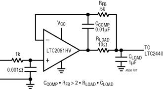
Figure 23.7 Basic Buffer for the LTC2440
The input noise of two LTC2051s is approximately equal to the input noise of the LTC2440 by itself, which means that the overall resolution is reduced by a factor of 2 (one effective bit) when both inputs are buffered.
Low noise bipolar amplifiers can be orders of magnitude quieter than chopper or autozero amplifiers at frequencies above the amplifier’s 1/f corner. Low frequency noise and drift are not a problem for AC applications, but may require canceling for high accuracy DC measurements. AC excitation cancels any DC error sources and allows for extremely high-resolution bridge measurements.
The circuit in Figure 23.8 uses the LT1678 low noise amplifier and correlated double sampling to achieve a single reading resolution of 14nVRMS. The amplifiers are compensated to drive 1μF capacitors at the inputs to the LTC2440. The 200nV input noise of the LTC2440 allows for a conservative gain of 21, thus reducing errors associated with finite amplifier gain and large output swings. Even rail-to-rail amplifiers tend to perform better when their outputs are far away from the rails; this circuit only produces a 210mV differential output for a full scale 10mV input, keeping both outputs happily close to mid-supply. This is in contrast to circuits that use an instrumentation amplifier with a gain of 500 in order to fill the entire input range of a lower resolution ADC—another major advantage of the LTC2440.

Figure 23.8 Single 5V Supply Circuit Resolves 1 Part in 200,000 Over a 10mV Strain Gauge Output Span
Reversing the excitation to the bridge produces several benefits. First of all, autozero amplifiers are not required to maintain DC accuracy, since all offsets are cancelled. Parasitic thermocouples are cancelled as well since these voltages appear in series with the amplifier offsets. If the signal wires from the sensor are of even slightly different composition, a thermocouple pair will result. Consider the case of two “identical” copper wires that have a thermoelectric potential of 0.2μV/°C. A “temperature noise” of 1°CRMS translates directly to 200nVRMS measurement noise (Linear Technology Application Note 86, Appendix J).
Bridge excitation switching is accomplished by brute force with two Si9801DY FET half bridges. While this may seem less elegant than driving the excitation with force/sense amplifiers, it eliminates the need for supply voltages outside of 0V and 5V and the errors introduced are far less than those of most very high quality sensors. The total RDS(ON) of 0.13Ω translates to a mere 0.037% full-scale error and the 5000ppm/°C temperature coefficient of RDS(ON) only causes −2ppm/°C drift when used with a 350Ω bridge. These errors will be almost three times less with a 1000Ω bridge.
Figure 23.9 shows the inputs to the LTC2440 and the state of BUSY pin, indicating when sampling is taking place.
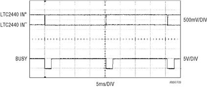
Figure 23.9 Amplifier Waveforms
How Many Bits?
A full-scale input of 10mV and an input noise of 14nVRMS gives 19.4 bits, noteworthy to the Marketing department. With this level of precision, the bridge itself is the dominant error source. Consider the Omega LC1001 series calibrated, temperature compensated load cells. This device has a full-scale error of 0.25%, a zero offset of 1% of full scale and a linearity of 0.05% of full scale. Temperature coefficient of both zero and span are 20ppm/°C. All of these errors can be calibrated out, including thermal drift if the temperature of the cell is measured. However, mechanical hysteresis and non-repeatability affect the maximum resolution that can be achieved under all conditions. The hysteresis specification for this load cell is 0.03% of full scale, or 1 part in 3333. This does not necessarily mean that this will be an “11.7-bit” system—it depends on the application. If this load cell is used in a parts counting scale, then it will be zeroed frequently and the load will be quickly applied and measured. Long term creep effects that lead to hysteresis will be negligible.
To illustrate the real resolution of the circuit in Figure 23.8, half a penny was dropped onto a Tedea model 1240 load cell with a 200kg full-scale range, equivalent to adding 1 part in 200,000. As Figure 23.10 shows, the additional weight is clearly registered.
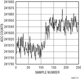
Figure 23.10 1 Gram Step

Figure 23.11 Correlated Double Sampling Frequency Response
Appendix A
Frequency response of an AC excited bridge
The AC excitation technique described in the last application circuit is actually a simple finite impulse response (FIR) filter. Any signal not caused by the excitation voltage (which includes all offsets and amplifier input noise) sees a 2-tap FIR filter with coefficients of (0.5, −0.5). This produces a null at DC, fS, 2fS, etc., and a gain of 1 (0dB) at fS/2, 3fS/2, 5fS/2, etc., and the frequency response is 0.5 −0.5 • COS(2π • f/fS).
Noise at 3.4Hz is not attenuated, but it actually isn’t quite so bad. The ADC’s own internal filter is down 3dB at the sampling frequency so the net gain is −3dB at 3.4Hz. Although 3.4Hz is below the amplifier’s 13Hz 1/f corner, it is still faster than any expected thermal effects.
The autozeroing process also affects the response of the input signal. Since the excitation reversal is calculated out in software, the result is a 2-tap FIR filter with coefficients of (0.5, 0.5). This produces a gain of 1 at DC, fS, 2fS, etc., and a null at fS/2, 3fS/2, 5fS/2, etc., and the frequency response is 0.5–0.5 • COS(2π • f/fS). This also reduces the bandwidth by a factor of 2, which reduces the noise by a factor of 2.
Since the LTC2440 input noise is Gaussian, averaging more samples further reduces the noise. (Noise is reduced by a factor of the square root of the number of readings averaged.) The optimum number of samples to average depends on the application—where the cost for additional noise reduction is increased settling time.
Appendix B
Measuring resolution, RMS vs peak-to-peak noise and psychological factors
When testing signal conditioning circuits, it is important to isolate error sources and be familiar with the limitations of the sensor. In the case of the circuit in Figure 23.8, the first test is to short the differential amplifier inputs together and bias them to mid-supply. This emulates a perfect load cell with zero offset and zero output impedance. In this configuration, the only output is the noise and offset of the circuit itself. Another test is to connect the inputs to a mid-supply bias through two 350Ω resistors, adding the effects of amplifier bias current and current noise.
The last test, before actually connecting the load cell, is to connect a DJ Instruments model DJ-101ST strain gauge bridge simulator. This instrument is a precision resistor bridge that simulates a strain gauge. Full-scale outputs of 1, 2, 3, 5, 10 and 15mV/V are provided, and for a given range the output can be adjusted from 0% to 120% of full scale in 10% steps. The objective is to emulate all of the properties of a strain gauge except measuring strain. This device verifies that Figure 23.8 maintains 19nVRMS resolution across its entire input range. The LT1461 was selected based on its low drift and high output current—there are more quiet references available, but this test shows that its noise performance is adequate. Applying a full-scale input will determine if the reference voltage is sufficiently quiet —a noisy reference will elevate ADC noise when the input is close to full scale. (The output code of an ADC is VIN/VREF. Thus noise in the output data that is due to reference noise is directly proportional to the input voltage, assuming the reference noise is small compared to VREF.)
The last test is to actually connect a load cell. This circuit will detect 1 gram on a Tedea model 1240 load cell with a 200kg capacity, and it will detect one sheet of copier paper dropped on a stack of 20 reams (10,000 sheets). The importance of testing the circuit with a bridge simulator becomes clear when the air conditioner turns on—a single sheet of paper gets buried in noise. This exposes a very real limitation on high resolution weigh scales; a large tare weight turns the scale into a very sensitive seismograph. Other limitations include mechanical hysteresis, creep and linearity of the load cell.
RMS vs Peak-to-Peak Noise
Another topic that often surfaces in high resolution applications is whether to use RMS noise or peak-to-peak noise. Some would eschew RMS noise as useless, asserting that peak-to-peak noise is the true measure of performance. However RMS noise has a distinct advantage—it is standardized and easy to calculate by taking the standard deviation of a set of ADC readings. This is only valid if the output noise is Gaussian, which is the case for all of Linear Technology’s delta sigma ADCs.
Consider a high resolution ADC that has 1μVRMS input noise and zero offset. With the inputs shorted together, it will produce a distribution of output values, 68.27% of which will be within 1μV of zero. Of course this implies that 31.73% of the readings are more than 1μV away from zero. It would be nice to know the true “peak-to-peak” noise of an ADC; some bound on the error for any given data point. But electrical noise does not work this way; there is always a nonzero probability that any one reading can have a value very far from the average. Fortunately there is a systematic way to relate the performance requirements of an application to the RMS noise level, but it does require a small dose of realism.
Say a weigh scale application requires 10,000 “counts” of resolution. If the load cell has a 10mV full-scale output, this implies a voltage resolution of 1μV. The LTC2440 has 200nVRMS input noise in its highest resolution mode, so it should work. But one common rule says that the ratio of peak-to-peak to RMS (also called crest factor) is 6 for Gaussian noise, so the peak-to-peak noise is 1.2μV— greater than the 1μV spec. The piece of information missing is the probability that a reading will be outside of the acceptable limit. If the noise at the ADC inputs is Gaussian, then the answer should lie in the normal error integral table found in the back of any statistics textbook.
Figure 23.12 shows 10,000 readings from an LTC2440 in the lowest noise mode (6.8 samples per second), and Figure 23.13 is a histogram of these readings that appears Gaussian at first glance.
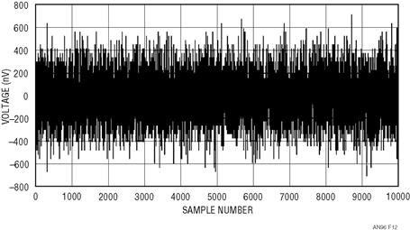
Figure 23.12
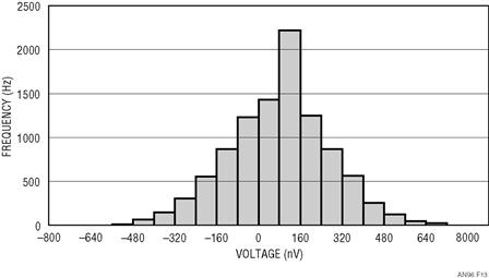
Figure 23.13
The RMS noise of this particular LTC2440 is 194nV, slightly better than the 200nV typical spec. Table 23.3 compares the textbook probability that a reading will be within a certain crest factor to the actual measured values.
Table 23.3
| CREST FACTOR | TEXTBOOKPROBABILITY (%) | MEASUREDPROBABILITY (%) |
| 2 | 68.27 | 70.95 |
| 3 | 86.64 | 85.12 |
| 4 | 95.45 | 95.66 |
| 5 | 98.76 | 98.83 |
| 6 | 99.73 | 99.76 |
| 7 | 99.95 | 99.98 |
This shows that the noise at the input of the LTC2440 is indeed very close to Gaussian. It also shows that only one reading in 100 will be outside of a ±0.5μV range. If the display shows 10,000 counts, one would have to stare at it for almost 15 seconds to see more than one count of noise. If this is acceptable, then assuming a crest factor of 5 is adequate and there is no need for additional signal conditioning. If it is not acceptable, follow the design procedure in the section on increasing resolution with amplifiers.
Psychological Factors
Linear Technology’s 20- and 24-bit ADCs have an LSB size that is smaller than the noise voltage (this is typical of any high resolution ADC). As a result, these devices will have a number of bits that do not hold steady for a constant input voltage. It is almost impossible to estimate ADC noise by looking at the binary data output. Looking at a decimal representation of the output data is not much better. In fact, the only way to get an objective opinion on the RMS noise level of a given circuit is to collect a set of data points and take the standard deviation.
This is a good lead-in to one last hint for designing circuits with Linear Technology’s delta sigma ADCs. Always provide an easy way to get data points into a PC. Even in a handheld application that will never be attached to a computer in real life, the ability to analyze data will save an incredible amount of troubleshooting time. A convenient way to do this is to send data to the PC’s serial port using the circuit shown in Figure 23.14.
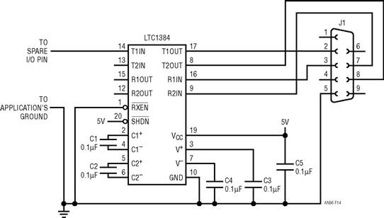
Figure 23.14 Serial Debug Circuit
Use a spare I/O pin to send the serial data and write a small test program that only takes data from the ADC and sends it to the PC. If all of the processor’s I/O pins are used up, pick one that can be safely used for this purpose in a “test mode,” such as a pin that normally reads the state of a pushbutton. It is not even necessary to use a hardware UART to generate the serial data; a simple “bit-bang” routine at 1200 baud will work just fine. Most compilers provide a printf or sprintf function to format data as ASCII decimal characters. If these are not available, then sending ADC data as eight ASCII hexadecimal characters will work as most spreadsheets provide a “HEX2DEC” function to convert hexadecimal to decimal data. Most operating systems have a terminal program included that is suitable for capturing data to a text file that can then be imported into a spreadsheet.
Appendix C
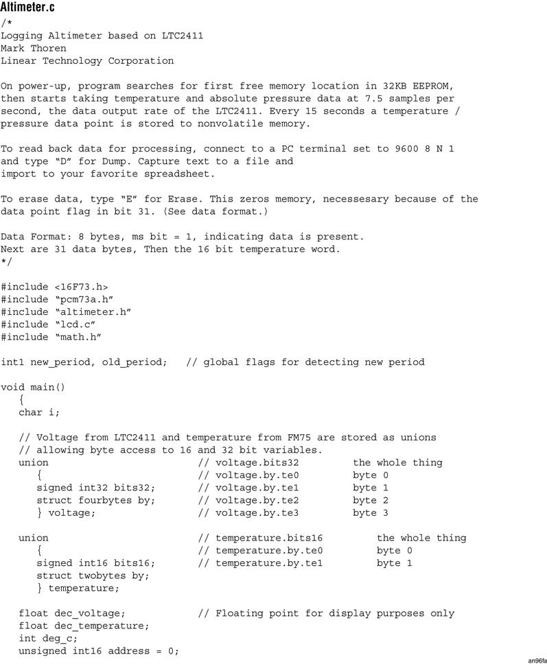
Altimeter code


Appendix D
Correlated double sampling driver code
Note 1Based on a 99.97% probability.