31
Take the mystery out of the switched-capacitor filter
The system designer’s filter compendium
Introduction
Overview
This chapter presents guidelines for circuits utilizing Linear Technology’s switched-capacitor filter family. Although the switched-capacitor filter has been designed into “telecom” circuits for over 20 years, the newer devices are faster, quieter and lower in distortion. These filters now achieve total harmonic distortion (THD) below −76dB (LTC®1064-2), wideband noise below 55μVRMS (LTC1064-3), high frequency of operation (LTC1064-2, LTC1064-3 and LTC1064-4 to 100kHz) and steep roll-offs from passband to stopband (LTC1064-1: −72dB at 1.5× fCUTOFF). These specifications make the new generation of switched-capacitor filters from LTC candidates to replace all but the most esoteric of active RC filter designs.
Chapter 40 takes the mystery from the design of high performance active filters using switched-capacitor filter integrated circuits. To help the designer get the highest performance available, this chapter covers most of the problems prevalent in system level switched-capacitor filter design. The chapter covers both tutorial filter material and direct operating criteria for LTC’s filter parts. Special attention is given to proper breadboarding techniques, proper power supply selection and design, filter response selection, aliasing, and optimization of dynamic range, noise and THD. These issues are presented after a short introduction to the switched-capacitor filter
The switched-capacitor filter
Why use switched-capacitor filters? One reason is that sampled data techniques economically and accurately imitate continuous time functions. Switched-capacitor filters can be made to model their active RC counterparts in the continuous time domain. The advantages of the switched-capacitor approach lie in the fact that a MOS integrated capacitor with a few switches replaces the resistor in the active RC biquad filter allowing full filter implementation on a chip. The building block for most filter designs, the integrator, appears in Figure 31.1. When implemented with resistors, capacitors and op amps it is expensive and sensitive to component tolerances. The switched-capacitor integrator, as seen in Figure 31.2, eliminates the resistors and replaces them with switched capacitors. The dependency on component tolerances is virtually eliminated because the switched-capacitor filter integrator depends on capacitor value ratios, and not on absolute values. This provides very good accuracy in setting center frequencies and Q values. Additionally, this implementation allows the effective resistor value to be varied by the clock operating the switches. This allows the resistors (and therefore the filter center frequencies) to be varied over a wide range (typically 10,000:1 or more). Since existing integrated circuit technology can implement capacitor ratios much more accurately than resistor ratios (see Figure 31.2), the switched-capacitor filter can provide filters with inherent accuracy and repeatability. Active RC configurations are limited by resistor and capacitor tolerances (and to a secondary extent, the accuracy and bandwidth of the op amps) and usually require trimming. Switched-capacitor filters do have disadvantages compared to their active RC competitors. These include somewhat more noise in some circuit configurations and a phenomenon called clock feedthru. Clock feedthru is circuit clock artifacts feeding through to the filter output. It is present in virtually all sampled data systems to some degree. LTC has greatly improved this parameter over the past few years to the point where clock feedthru in the LTC1064 series is rarely a problem.

Figure 31.1 Active RC Inverting Integrator

Figure 31.2 Inverting Switched-Capacitor Integrator
Present day switched-capacitor filters include one to four 2nd order sections per packaged integrated circuit. Not long ago the switched-capacitor filter was only considered for low frequency work where signal-to-noise ratio was non-critical. This has changed for the better in recent years. Recent switched-capacitor filter designs allow up to 8th order switched-capacitor filters to be implemented that compete successfully with the typical multiple operational amplifier designs in critical areas, including signal-to-noise ratios, stopband attenuation and maximum cutoff frequencies.1
Circuit board layout considerations
The most critical aspect of the testing and evaluation of any switched-capacitor filter is a proper circuit board layout. Switched capacitor filters are a peculiar mix of analog and digital circuitry that require the user to take time to lay out the circuit board, be it a breadboard or a board for the space station. All this hoopla is standard “do as I say, not as I do” in most data sheets. To give this issue its proper credibility, two breadboards were built of the same circuit. The first was built on a “protoboard.” No bypass capacitors were used to isolate the power supply from the circuitry and, of course, there was no ground plane. The clock line consisted of flying wires as opposed to the coax used on the second or “recommended” breadboard. Additionally, when tests were run on the first breadboard, in most cases, no buffer operational amplifier at the filter output was used. A photograph of the first protoboard breadboard is shown as Figure 31.3. It should be emphasized here that the protoboard is a very good board for some types of breadboarding scenarios; it is just not very useful for the type of layout a switched-capacitor filter circuit requires.

Figure 31.3 Improperly Constructed “Poor” Switched-Capacitor Filter Breadboard
Figure 31.5 shows a photograph of a properly constructed switched-capacitor filter breadboard. The circuit is built on a copper clad board which acts as a ground plane. The switched-capacitor filter and buffer operational amplifier are well bypassed. All leads are kept as short as possible and the switched-capacitor filter clock input is through a shielded cable. The second breadboard uses a single point ground in the form of the whole board. (Figure 31.4 shows the schematic for both breadboards.) Single point grounding techniques become more and more critical as switched-capacitor filter parts are incorporated into large boards containing many analog and digital devices. In these large boards, and in larger multi-board systems, lots of design time should be spent on single point grounding techniques and noise abatement.2–6 It will be worthwhile in the long run.

Figure 31.4 Schematic of LTC1064-1 Breadboards

Figure 31.5 Properly Constructed “Good” Switched-Capacitor Filter Breadboard
Test results comparing the same circuit built on each breadboard are very interesting. Figure 31.6 shows the passband response of an 8th order Elliptic lowpass filter, the LTC1064-1. The figure clearly illustrates the ripple in the passband that can be attributed not to the filter, but to the breadboarding technique. The good breadboard is a factor of 5 to 10 times better than the inadequate breadboard.

Figure 31.6 Passband Response—8th Order Elliptic Lowpass Filter (LTC1064-1). Top Trace: Improperly Constructed Breadboard, No Buffer. Bottom Trace: Good Breadboard, with Buffer. Both: fCLK = 2MHz, fCUTOFF = 20kHz, VS = ±8V. Note: Top Trace Was Offset to Increase Clarity
Figure 31.7 shows the two breadboard circuits measured in the filter stopband. The top trace is the inadequate breadboard while the bottom is the well constructed model. Note the loss of between 10dB and 20dB of attenuation. Also notice the notch, almost 80dB down from the input signal, which is clearly shown when using a good breadboard and which cannot be seen using the poorly constructed breadboard.

Figure 31.7 Stopband Response—8th Order Elliptic Lowpass Filter (LTC1064-1). Top Trace: Improperly Constructed Breadboard, No Buffer. Bottom Trace: Good Breadboard, with Buffer. Both: fCLK = 2MHz, fCUTOFF = 20kHz, VS = ±8V
Figures 31.8 and 31.9 show the noise for the two different breadboards. Two plots were necessary as the noise was more than an order of magnitude greater when the poor breadboard was used. These tests were run using the identical switched-capacitor filter part (LTC1064-1CN) which was moved from one breadboard to the next to ensure exactly the same measurement conditions, except for the breadboards themselves.

Figure 31.8 Wideband Noise Measurement—8th Order Elliptic Lowpass Filter (LTC1064-1) Using Improper Breadboarding Techniques. fCLK = 2MHz, fCUTOFF = 20kHz, VS = ±8V, Buffered with LT1007

Figure 31.9 Wideband Noise Measurement—8th Order Elliptic Lowpass Filter (LTC1064-1) Using Good Breadboarding Techniques. fCLK = 2MHz, fCUTOFF = 20kHz, VS = ±8V, Buffered with LT1007
Not shown graphically, but measured, was the offset voltage of the switched-capacitor filter part in each breadboard. In the poorly constructed board the offset was a whopping 266mV, while in the other circuit board it was 40.7mV, almost a factor of seven times less.
Carefully note that all measurements in this Application Note (with a few noted exceptions) were performed with a good 10×, low capacitance, scope probe (i.e., Tektronix P6133) at the output of the buffer operational amplifier. The probe ground lead length was kept below 1″ in length.
Moral of this section: Beware the breadboard that sits on your bench. It may not suffice to resurrect your old 741 breadboard to test today’s switched-capacitor filters. They require fast clocks, buffering and good breadboarding techniques to deliver their optimum specifications.
Power supplies
Power supplies, proper bypassing of these supplies, and supply noise are usually given little attention in the board spectrum of chaos called system design. Beware! Sampled data devices such as switched-capacitor filters, A-to-D and D-to-A converters, chopper-stabilized operational amplifiers and sampled data comparators require careful power supply design. Poorly chosen or poorly designed power supplies may induce noise into the system. Similarly, improper bypassing may impair even the most ideal of power supplies. Common complaints range from noise in the passband of a switched-capacitor filter to spurious A-to-D outputs due to high frequency noise being aliased back into the signal bandwidth of interest. These effects are, at best, difficult to find and, at worst, worth a call to the local goblin extermination crew (LTC’s Application Group!).
Figure 31.10 shows an example of how a switcher can cause problems. The figure was generated by using the breadboard in Figure 31.3. An industry standard 5V to ±15V switcher module was used to power the board. The switcher was unbypassed to better illustrate the potential problems.

Figure 31.10 Stopband Response—8th Order Elliptic Lowpass Filter (LTC1064-1). Power Supply is Unbypassed Industry Standard Modular 5V to ±15V Switcher. The Improperly Constructed Breadboard Was Used for This Test. fCLK = 2MHz, fCUTOFF = 20kHz, VS = ±7.5V (Switched Zenered to ±7.5V)
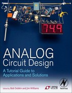
Figure 31.10 can be compared directly with Figure 31.7 to see the switcher noise. The poor breadboard causes the stopband attenuation to be well above where it should be when proper breadboarding techniques are used but switcher harmonics are also evident. These appear in Figure 31.10. Some of these peaks are only −45dB down from the signal of interest in the passband and could be confused with a legitimate signal. Clearly, if a filter is designed to be 80dB down in the stopband, using a noisy switcher will not do. Figure 31.11 shows the schematic diagram of a good, low noise switcher for system use. It produces ±7.5V with 200μV of noise. The switcher is an excellent example of good, low noise design techniques.7
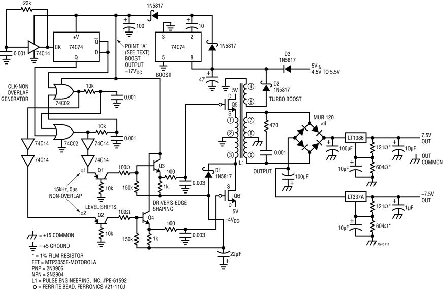
Figure 31.11 Low Noise 5V to ±7.5V Converter (200μVP-P Noise)
All power supplies in a good system design should be properly bypassed. There are as many techniques for bypassing as voodoo curses, so we will not overly dwell on the subject. For switched-capacitor filters, we recommend good, low ESR bypass capacitors (0.1μF minimum, 0.22μF better) as close to the power supply pins of the part as possible. High quality capacitors are recommended for bypassing. For more details on how to identify an adequate capacitor see Appendix B. We recommend separate digital and analog grounds with the two only being tied together as close to supply common as practical. The ground lead to the bypass capacitors should go to the analog ground plane.
The prudent layout includes bypass capacitors on the pins of the switched-capacitor filter which are tied to a circuit potential for programming, such as the 50/100 pins. Should spikes and/or transients appear on this pin, trouble will ensue. The summing junction pins SA, SB, etc., are also candidates for bypassing if they are tied to analog ground in a single supply system where lots of noise is present. This last issue is probably icing on the cake in most cases, but it will help lower the noise in some cases.
Last, but not least, the power supplies used to power the switched-capacitor filters limit the maximum input and output signals to and from the filters. Thus, power supplies have a direct effect on the system dynamic range. For the LTC1064 type filter ±7.5V supplies provide ±5V output swing, while ±5V supplies provide ±3.3V of swing. For a filter with 450mVP-P of output noise these numbers translate to 87dB and 83dB of dynamic range respectively.
Input considerations
This section considers some aspects of switched-capacitor filter design which are related to the input signal, the filter’s input structure and the overall filter response.
Offset voltage nulling
Typical offset voltages for an LTC1064 or an LTC1064-X through the four sections may range up to 40mV or 50mV. While this may not be of concern for AC-coupled systems, it becomes important in DC-coupled applications. The anti-aliasing filter used before an A/D converter is a typical application where this is an important concern. For a 5VO-P input signal, the least significant bit of an 8-bit A/D converter is approximately 20mV, and one-half the LSB is approximately 10mV. This implies that use of a filter (or for that matter, any type of device other than a straight wire) before an 8-bit A/D converter requires offset voltages below 10mV. For a 12-bit converter this provision mandates stringent 600μV of offset at the A/D’s input.
Several methods of offset cancellation are common. The usual method seen with operational amplifiers utilizes a potentiometer to inject a correction voltage. Figure 31.12 shows this arrangement with an LTC1064-1 Elliptic filter. This method can correct the initial offset, but both the adjustment circuit and the CMOS operational amplifiers in the switched-capacitor filters have temperature coefficients that are not zero. Thus, if this circuit is used to correct the offset at 25°C, it will not fully correct the offset at another temperature. An advantage of this type of offset nulling is that the filter’s frequency response is affected very little. Figure 31.13 shows the time domain response of Figure 31.12’s filter circuitry. The rising and falling edge overshoot is typical of high Q filters be it switched capacitor or active RC. (This time domain performance parameter, the rise time, is treated separately in a later section.) Compare Figure 31.13 with Figure 31.15 to observe the time domain response of an open-loop offset correction scheme (the potentiometer) versus Figure 31.14’s closed-loop servo.

Figure 31.12 Elliptic Filter with Offset Adjustment Potentiometer

Figure 31.13 Time Domain Response of Elliptic Filter (LTC1064-1) Without Servo in Figure 31.12. Input Signal 1Hz Square Wave. LTC1064-1 Cutoff (fO) = 100Hz. Horiz = 0.1s/Div., Vert = 0.5V/Div (Photograph Reproduction of Original)
Figure 31.14 Elliptic Filter (LTC1064-1) with Servo Offset Adjustment
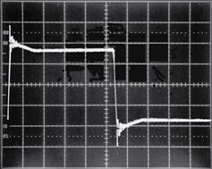
Figure 31.15 Time Domain Response of Elliptic Filter (LTC1064-1) with Servo per Figure 31.14. Input Signal 1Hz Square Wave. LTC1064-1 Cutoff (fO) = 100Hz. Horiz = 0.1s/Div., Vert = 0.5V/Div (Photograph Reproduction of Original)
Figure 31.14 shows the circuit of an LTC1064-1 Elliptic filter with the same LT1007 output buffer amplifier used in Figure 31.13. An addition is the LT1012 operational amplifier used as a servo to zero the offset of the filter. This arrangement can provide offsets of less than 100μV which is quite acceptable for a 12-bit system. The servo generates a low frequency pole at about 0.16Hz which can interact with some signals of interest to some system users. Figure 31.15 shows the low frequency square wave response. Figure 31.16 shows the distortion introduced for large-signal inputs at a frequency near the servo pole. Figure 31.17 shows a sine wave input to the servo system, but at lower amplitude and higher frequency. The small distortion introduced at this higher frequency is probably traceable to the servo’s high frequency cutoff. Figure 31.19 shows the servo response to the small-signal input at 0.092Hz shown in Figure 31.18. The servo tracks this input, but at a lower amplitude. The servo thus looks like a highpass filter to the input signal at input frequencies below the servo pole frequency. Servo offset nulling can be extremely useful in systems if the limitations described are tolerable.
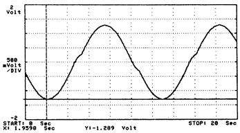
Figure 31.16 Large-Signal Response—Output of Elliptic Filter (LTC1064-1) Plus Servo (Figure 31.14). Input: 1VRMS, 0.092Hz Sine Wave. Filter fCUTOFF = 100Hz
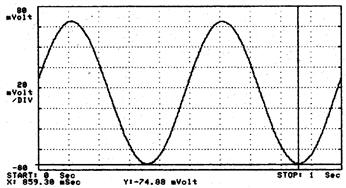
Figure 31.17 Small-Signal Response—Output of Elliptic Filter (LTC1064-1) Plus Servo (Figure 31.14). Input: 50m VRMS, 2Hz Sine Wave. Filter fCUTOFF = 100Hz

Figure 31.18 Input Signal (50mVRMS, 0.092Hz) to Elliptic Filter (LTC1064-1) as Shown in Figure 31.14
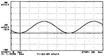
Figure 31.19 Small-Signal Output Response of Elliptic Filter (LTC1064-1) Plus Servo to Input Shown as Figure 31.18. Filter fCUTOFF = 100Hz
Slew limiting
The input stage operational amplifiers in active RC or switched-capacitor filters can be driven into slew limiting if the input signal frequency is too high. Slew limiting is usually caused by a capacitance load drive limitation in the op amps internal circuitry. Contemporary switched-capacitor filter devices are designed to avoid slew limiting in almost all cases.8
As an example, the LTC1064 filter has a typical slew rate of 10V/μs. Since slew rate is a large-signal parameter, it also defines what is called the power bandwidth, given as:
![]()
where fP is the full power frequency and EOP is the peak amplifier output voltage.
For the LTC1064 operating at VS = ± 7.5V the device can swing ±5V or 10V peak. Based on the op amp slew rate performance only, the full power frequency is calculated as:
![]()
This fP is sufficient for all but the most stringent switched-capacitor filter applications of the LTC1064.
Aliasing
Since the switched-capacitor filter is based around a “switching capacitor” to generate variable filter parameters, it is by definition a sampled data device. Like all other such devices it is subject to aliasing. Aliasing is a complex subject with lots of mathematics involved. As such, its derivation is the subject of many paragraphs in textbooks.9 The system designer can get a meaningful handle on the subject by a series of spectrum analyzer views.
Figure 31.20 through Figure 31.23 each show three spectrum segments while the switched-capacitor filter’s input signal varies from 100Hz to 49.9kHz. Each figure shows a different input frequency and spectrum plots of the filter’s passband (10Hz to 510Hz), the frequency spectrum around fCLK/2 (25kHz) and the frequency spectrum around fCLK (50kHz). The switched-capacitor filter is a lowpass elliptic filter (LTC1064-1) with a cutoff frequency set to 500Hz (fCLK/fCUTOFF = 100:1). The clock used for this cutoff is 50kHz. Thus, from sampled data theory, aliasing begins when the input signal passes the fCLK/2 threshold (25kHz).

Figure 31.20 Elliptic Switched-Capacitor Filter (LTC1064-1) Aliasing Study. fO = 500Hz, fCLK = 50kHz, VS = ±8V, VIN = 100Hz at 500mVRMS. Note Dynamic Range Limitation
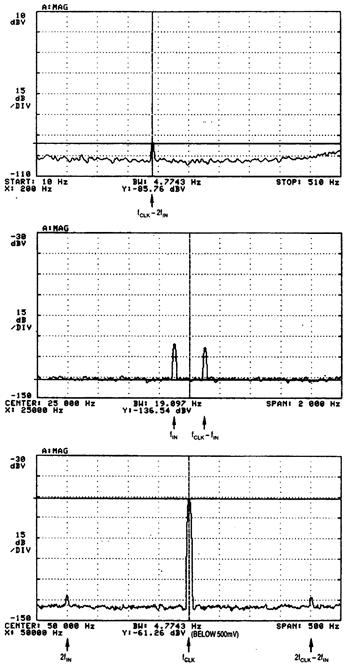
Figure 31.21 Elliptic Switched-Capacitor Filter (LTC1064-1) Aliasing Study. fO = 500Hz, fCLK = 50kHz, VS = ±8V, VIN = 24.9kHz at 500mVRMS

Figure 31.22 Elliptic Switched-Capacitor Filter (LTC1064-1) Aliasing Study. fO = 500Hz, fCLK = 50kHz, VS = ±8V, VIN = 25.1kHz at 500mVRMS

Figure 31.23 Elliptic Switched-Capacitor Filter (LTC1064-1) Aliasing Study. fO = 500Hz, fCLK = 50kHz, VS = ±8V, VIN = 49.9kHz at 500mVRMS. Note Dynamic Range Limitation
Figure 31.20 shows the LTC1064-1 in its normal mode of operation with the signal (100Hz) within the passband of the filter. Note the small second harmonic content (−80dB) component which also appears in the passband.
No signals are seen around fCLK/2, however, the original signal (100Hz) appears attenuated (sin x/x envelope response) at 49.9kHz and 50.1kHz. This is consistent with sampled data theory and is a very important anomaly to be taken into consideration in some systems. Thus, for any signal input there will be side lobes at fCLK ± fIN. These side lobes will be attenuated by the sin x/x envelope familiar to those who work with sampled data systems.
Figure 31.21 shows the same series of spectral photos for an input signal of 24.9kHz. This signal is outside of the filter passband, so the signals are much attenuated. The signal seen at 200Hz in this series of plots is actually the alias of the 49.8kHz second harmonic of the input signal. The signals seen around 25kHz are the 24.9kHz input and the fCLK - fIN signals (see your textbook)!! The signals around and at 50kHz are clock feedthru, and the second harmonic images of the 24.9kHz input signal around the clock frequency.
Similarly, Figure 31.22 shows spectral plots for an input signal of 25.1kHz. The signals appear in the same locations as Figure 31.21, but for different reasons. The 200Hz signal in this figure is the alias of the 50.2kHz. The signals around 25kHz are the input signal at 25.1kHz and its alias at 24.9kHz.
Figure 31.23 details aliasing at its very worst. The input signal here is 49.9kHz which aliases back, in the filter passband, to 100Hz and appears almost identical to Figure 31.20’s 100Hz signal. The input signal appears at 49.9kHz with its 50.1kHz mirror image.
Of additional note to the system designer is the LTC1062 5th order dedicated Butterworth lowpass filter. This device makes use of a continuous time input stage (an R and C) to prevent aliasing, making it attractive in some applications.
Filter response
What kind of filter do I use? Butterworth, Chebyshev, Bessel or Elliptic
One of the questions most asked among system designers at the shopping malls of America is “how do I choose the proper filter for my application?” Aside from the often used retort, “call Linear Technology,” a discussion of the types of filters and when to use them is appropriate.
A typical application could involve lowpass filtering of pulses. This filter might be in the IF section of a digital radio receiver. The received pulses must pass through the filter without large amounts of overshoot or ringing. A Bessel filter is most likely the filter of choice.
Another application may be insensitive to filter pulse response, but requires as steep a cutoff slope as possible. This might occur in the detection of a series of continuous tones as in an EEG system. If filter ringing is irrelevant, an Elliptic filter may be a good choice.
The trade-offs involved in filter design are critical to the system designer’s understanding of this topic. This means understanding what happens in both the time domain and in the frequency domain. At the risk of sounding pedantic, a discussion of this topic is appropriate. A time domain response can be viewed on an oscilloscope as amplitude versus time. It is in the time domain that pulse overshoot, ringing and distortion appear. The frequency domain (amplitude versus frequency) is traditionally where the designer looks at the filter’s response (on a spectrum analyzer). A wonderful response in the frequency domain often appears ugly in the time domain. The converse may also be true. It is crucial to examine both responses when designing a filter!
Figures 31.24 through 31.28 reprinted here from Zverev10 show the time domain step response for the Butterworth, two types of Chebyshev, a Bessel and a synchronously tuned filter. (The synchronously tuned filter is one that is made up of multiple identical stages, but contains no notches. See AM27A for more discussion on this topic.) Figure 31.29 shows the time domain response of the LTC1064-1 8th order Elliptic LP filter to a 10Hz input square wave. The photo shows that a system requiring good pulse fidelity cannot use this filter. Figure 31.30 shows a better filter for this application. It is the LTC1064-3, an 8th order Bessel LPF. The response has a nice, rounded off rise time with no overshoot. The trade-off appears in the frequency domain.

Figure 31.24 Step Response for Butterworth Filters*
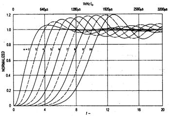
Figure 31.25 Step Response for Chebyshev Filters with 0.1dB Ripple*

Figure 31.26 Step Response for Chebyshev Filters with 0.01dB Ripple*

Figure 31.27 Step Response for Maximally Flat Delay (Bessel) Filters*

Figure 31.28 Step Response for Synchronously Tuned Filters*

Figure 31.29 LTC1064-1 Time Domain Response. Filter fCUTOFF = 100Hz. Input: 10Hz Square Wave. Horiz = 20ms/Div., Vert = 0.5V/Div (Photograph Reproduction of Original)
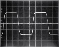
Figure 31.30 LTC1064-3 Time Domain Response. Filter fCUTOFF = 100Hz. Input: 10Hz Square Wave. Horiz = 20ms/Div., Vert = 0.5V/Div (Photograph Reproduction of Original)
Figures 31.31 through 31.34 show the frequency domain response of four 8th order filters, the LTC1064-1 through LTC1064-4. (Figure 31.35 shows an expansion of the comparison of the LTC1064-1 and LTC1064-4 roll off from the passband to the stopband.) The LTC1064-1 and LTC1064-4 are 8th order Elliptic filters, while the LTC1064-2 is a Butterworth and the LTC1064-3 is a Bessel. The roll-off from the passband to the stopband is least steep for the LTC1064-3 Bessel filter. This is the price paid for the linear phase response which enable the filter to pass a square wave with good fidelity. Similarly, the LTC1064-2 Butterworth trades slightly worse transient response for steeper roll-off.

Figure 31.31 Frequency Domain Response of LTC1064-1 Elliptic Filter. fCUTOFF = 10kHz, VS = ±7.5V, LT1007 Output Buffer, 100:1
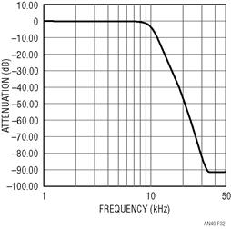
Figure 31.32 Frequency Domain Response of LTC1064-2 Butterworth Filter. fCUTOFF = 10kHz, VS = ±7.5V, LT1007 Output Buffer, 50:1

Figure 31.33 Frequency Domain Response of LTC1064-3 Bessel Filter. fCUTOFF = 10kHz, VS = ±7.5V, LT1007 Output Buffer, 75:1
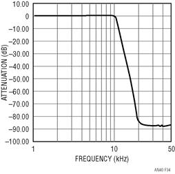
Figure 31.34 Frequency Domain Response of LTC1064-4 Elliptic Filter. fCUTOFF = 10kHz, VS = ±7.5V, LT1007 Output Buffer, 50:1
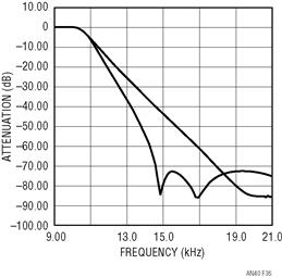
Figure 31.35 Frequency Domain Response of LTC1064-1 and LTC1064-4 Transition Region Blow-Up. fCUTOFF = 10kHz, VS = ±7.5V, LT1007 Output Buffer
The system designer must carefully consider a potential filtering solution in the time and frequency domains. Figures 31.24 through 31.34 are intended as examples to help the designer with this process. There are an infinite variety of filters that can be implemented with switched-capacitor filters to obtain the precise response required for one’s system.
Call Linear Technology Applications at (408) 432-1900 for additional help in choosing and/or defining a particularly difficult filtering problem.
The perennial question, “how fast can I sweep?” a filter from one frequency to another can be answered by looking at the transient response curves and renormalizing them to the desired cutoff frequency. Then the settling time can be read off the curve. A frequency sweep is in many aspects like the settling time performance to a pulse point.
Table 31.1 details the four filters mentioned previously and some of their key parameters. Note the wide variation in the stopband attenuation specification. This specification is a measure of the filters steepness of attenuation. This is a key specification for anti-aliasing filters found at an A/D converter’s input. Note that for the LTC1064-1 in the figure (corner frequency set to 10kHz) the attenuation to a 15kHz signal would be about 72dB. The Butterworth gives approximately 27dB, while the Bessel only about 7dB attenuation. These latter two filters trade frequency domain roll off for good time domain response.
Table 1 Filter Selection Guide

*These specifications from LTC data sheets represent typical values. Optimization may result in significantly better specifications. Call LTC for more details.
Filter sensitivity
How stable is my filter?
One of the great advantages of the switched-capacitor filter is the lack of discrete capacitors with their inherent tolerance and stability limitations. The active RC filter designed with theoretical capacitor values has problems with repeatability and stability when real world capacitors are used. The switched-capacitor filter has small errors in both the cutoff frequency, fO and Q, but they are easier to deal with than those of the active RC filter.
Most universal switched-capacitor filters are arranged in the so called State-Variable-Biquad circuit configuration.11 This configuration not only allows realization of all filter functions, LP, BP, HP, AP and notch, but also allows high Q filters to be realized with low sensitivity to component tolerances. (For a strict mathematical analysis of the sensitivity of the State-Variable-Biquad see reference 11, chapter 10.)
Manufacturing realities of the semiconductor business also affect the switched-capacitor filter design. Though this inaccuracy is much less than the active RC design (do the math in Daryanani) it does exist. Thus, switched-capacitor filters are available from manufacturers such as LTC with center frequency tolerances of generally 0.4% to 0.7%. This presumes an accurate stable clock. Operating the universal switched-capacitor filter in Mode 3 tends to make the center frequency error depend on the resistors since the equation for fO is:
![]()
Thus the manufacturing inaccuracy of the switched-capacitor filter is multiplied (and generally swamped) by the resistor inaccuracy. Mode 2 guarantees a filter designed with switched-capacitor filters has lower fO sensitivity than Mode 3 by changing the equation for fO to:
![]()
Here resistor sensitivity is mitigated by the one under the radical, and thus the inaccuracy is, in most cases, only caused by the manufacturing tolerances of the switched-capacitor filter. (See discussion of switched-capacitor filter modes in the LTC1060 and/or LTC1064 data sheets).
An excellent method of minimizing the filter dependence on resistor tolerances is to integrate the resistors directly on the semiconductor device. This can be done with the LTC1064 family of devices using silicon chrome resistors placed directly on the die.
Actual resistor values are generally better than 0.5%, but the important feature is that all thin film resistors track each other in both resistance and temperature coefficient. Thus, filters such as the LTC1064-1 through LTC1064-4 have virtually indistinguishable characteristics for each and every part.
The small tolerances in fO using the switched-capacitor filter are trivial when compared to an active RC filter. An Elliptic filter like the LTC1064-1 requires no small amount of trimming when built with resistors, capacitors and op amps. Changing the fO is even more impractical.
Output considerations
THD and dynamic range
Presently, one of the biggest uses of filters is before A/D converters for antialiasing. The filter band limits the signal at the input to a Digital Signal Processing system. A critical concern is the filter’s signal-to-noise ratio (SNR). Thus, if a filter has a maximum output swing of 2VRMS with noise of 100μVRMS it can be said to have an SNR (signal-to-noise ratio) of 86dB. This certainly seems to make it a candidate for antialiasing applications before a 14-bit A/D (required SNR approximately 84dB). But, is this the only consideration?? What is missing in this analysis is a discussion of total harmonic distortion. This is a frequently ignored subtlety of system design.
This filter example has an SNR or 86dB. But suppose its THD is only −47dB. What this means can be better understood by applying a 1kHz signal to the system. What is desired is to digitize this 1kHz to 14-bits of accuracy. What happens is quite different. The 1kHz signal, along with its harmonics, will be digitized. THD (total harmonic distortion) is a measure of the unwanted harmonics that are introduced by nonlinearities in the system. Thus, the 1kHz pure tone will come out looking like 1kHz + 2kHz + 3kHz, etc. The A/D converter will digitize these signals adding errors to the data acquisition process.
Figure 31.36 illustrates a good way to characterize this potential problem. This figure shows a THD plot of an LTC1064-2 8-pole Butterworth LPF (circuit as shown in Figure 31.37). The graph shows THD versus input amplitude. A second horizontal scale labels SNR. The graph clearly shows, for instance, that for a 1.5VRMS input the THD is below −70dB and the SNR is below −85dB. Thus, all the harmonics of the input signal (in this case 4kHz) are below −70dB. Figure 31.38 shows a THD + N versus frequency curve for the same filter. At an input frequency of 2kHz the THD + N is approximately 0.018% or −74.9dB. Figure 31.39 shows good correlation with a spectrum analyzer in the frequency domain. Of course, there are an unlimited number of these plots that can be taken, for an almost unlimited number of cutoff frequencies and input frequencies. What must be considered as the most important issue is that THD generally limits digitization accuracy, not SNR. Figure 31.40 shows four units of the LTC1064-2 with a 1kHz input frequency. Here, as before, the −70dB THD specification is preserved up to 2.5VRMS input.

Figure 31.36 LTC1064-2 THD + Noise vs Input Amplitude and Signal-to-Noise Ratio. Filter fCUTOFF = 8kHz, fIN = 4kHz, fCLK = 800kHz, VS = ±5V. Inverting Buffer LT1006
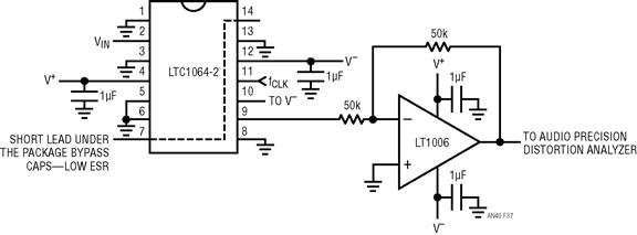
Figure 31.37 LTC1064-2 Circuit Used for THD Testing. VS = ±5V

Figure 31.38 LTC1064-2 THD + Noise vs Input Frequency. Filter fCUTOFF = 8kHz, fCLK = 800kHz, VS = ±5V, VIN = 1.5VRMS, Buffered Output Using LT1006
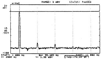
Figure 31.39 LTC1064-2 Spectrum Analyzer Plot for VIN = 1.5VRMS, fIN = 2kHz, VS = ±5V, Buffered Output Using LT1006

Figure 31.40 LTC1064-2 THD + Noise vs Input Amplitude and Signal-to-Noise Ratio. Filter fCUTOFF = 8kHz, fCLK = 800kHz, fIN = 1kHz, VS = ±5V, Inverting Buffer Using LT1006. Four Devices Superimposed
Total harmonic distortion is a complicated phenomenon and is difficult to analyze all its potential causes. Some of these causes in the switched-capacitor filter are thought to be the charge transfer inherent in the SC process, the output drive and the swing internal to the switched-capacitor filter state variable filter.
THD in active RC filters
THD in RC active filters is generally assumed to be superior to switched-capacitor filters. Traditional filter textbooks seem to lack data on THD, either in a theoretical or a practical sense. The data presented here shows the RC active to be somewhat better than the switched-capacitor filter, but at a tremendous cost in terms of board space, non-tunability and cost.
Figure 31.41 shows a THD versus amplitude plot of the RC active equivalent of the LTC1064-1 8th order Elliptic filter. This filter requires 16 operational amplifiers, 31 resistors and eight capacitors on a board approximately 2-1/2 × 6 inches in size. An equivalent THD plot for the LTC1064-1 is shown in Figure 31.42.
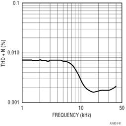
Figure 31.41 Active RC Implementation of LTC1064-1 8th Order Elliptic Filter. VIN = 3VRMS, VS = ±7.5V, Op Amps = TL084, fC = 40kHz
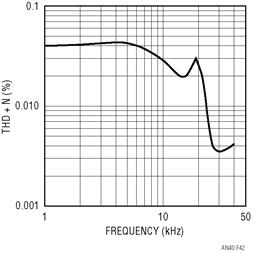
Figure 31.42 LTC1064-1 8th Order Elliptic Filter, VIN = 3VRMS, VS = ±7.5V, fC = 40kHz, Buffered Output
The Elliptic filters are the worst choice for good THD specifications because of their high Q sections. Butterworth and Bessel filters have very good THD specifications.
Linear Technology has done extensive research in comparing the THD and SNR aspects of our switched-capacitor filters to those of active RC filters. In many cases, a filter may be optimized for THD by adjusting its design parameters. This process is specialized and thus data sheet THD specifications may not reflect the best achievable. Call us for more details.
Noise in switched-capacitor filters
Noise in switched-capacitor filters has been on the decline since the invention of the device. At this time many devices, like the LTC1064 family, have noise which competes with active RC filters. What is not immediately obvious is that the noise of the switched-capacitor filter is constant independent of bandwidth. The LTC1064-2 Butterworth filter has approximately 80μVRMS noise from 1Hz to 50kHz (fO equal to 50kHz), it also has 50μVRMS noise from 1Hz to 10kHz (fO equal to 10kHz). Since the traditional RC active filter has noise specifications based on so many nV per Hz12, the switched-capacitor filter is a better competitor to the active RC as the filter cutoff frequency increases. Future LTC devices will have even better noise specifications than the LTC1064-2.
Figure 31.43 compares noise between an RC active equivalent of the LTC1064-1 and the switched-capacitor filter. Both curves show typical peaking at the corner frequency. The illuminating feature seen in this figure is that the TL084 active filter noise is only slightly better than the LTC1064-1.

Figure 31.43 Noise Comparison Between Figure 31.41 Active RC Elliptic B and LTC1064-1 A, Figure 31.42
Bandpass filters and noise—an illustration
Figure 31.44 is the frequency response of an 8th order Bessel bandpass filter implemented with an LTC1064 as shown in Figure 31.45. This filter has a Q of approximately nine and a very linear phase response (in the passband) as shown in Figure 31.47. As previously discussed, the Bessel response is very useful when signal phase is important.

Figure 31.44 8th Order Bessel Using LTC1064. VS = ±8V, VIN = 1VRMS, fCLK = 50kHz, fCUTOFF = 1kHz, Buffered Output

Figure 31.45 Implementation, Section by Section, of Bessel BPF as per Figure 31.43 Using LTC1064. For fCUTOFF = 1kHz, fCLK = 50kHz
Of particular interest to the present discussion is the noise of this bandpass filter (Figure 31.46). Note that the noise bandshape is identical to Figure 31.44. This is not unusual since the bandpass filter is letting only the noise at a particular fC through the filter This is not clock feedthru and it is not peculiar to the switched-capacitor filter. In an active RC, or even an LC passive bandpass filter with these characteristics, noise appears “like a signal” at the center frequency of the BPF.12

Figure 31.46 Noise Spectrum of Bessel BPF as Shown in Figure 31.43. Input Grounded. Total Wideband Noise = 130μVRMS

Figure 31.47 Passband Phase Response of Bessel BPF as Shown in Figure 31.43. Note the Linear Phase Through the Passband
Clock circuitry
Jitter
Clocking of switched-capacitor filters cannot be taken for granted. A good, stable clock is required to obtain device performance commensurate with the data sheet specifications. This implies that 555 type oscillators are verboten. Often, what appears as insufficient stopband attenuation or excessive passband ripple is, in fact, caused by poor clocking of the switched-capacitor filter device.
Figure 31.48 shows the LTC1064-1 set up to provide cutoff frequency of 500Hz. The clock was modulated (in the top curve measurement) to simulate approximately 50% clock jitter. The stopband attenuation at 750Hz is seen to be approximately 42dB instead of the specified (in the LTC1064-1 data sheet at 1.5× the cutoff frequency) 68dB. The second curve on the graph shows the situation when a good stable clock is used.

Figure 31.48 Clock Jitter of Approximately 50% (Top Curve in Stopband) and Jitter-Free Clock (Bottom Curve in Stopband) Showing the Difference in Response. LTC1064-1, fCLK = 50kHz, fO = 500Hz, Buffered Output
Similar graphs of the noise in Figures 31.49 and 31.50 show the effect of clock jitter on the noise. The wideband noise from 10Hz to 1kHz rises when a jittery clock is used from 156μVRMS to 173μVRMS. This is an increase of approximately 11% due only to a poor clocking strategy.

Figure 31.49 Noise of LTC1064-1 as per Figure 31.48 with ≈50% Clock Jitter. VS = ±7.5V, Input Grounded

Figure 31.50 Noise of LTC1064-1 as per Figure 31.48 with Low Jitter (<1ns). VS = ±7.5V, Input Grounded
LTC’s Application Note 12 provides some good clock sources if none are available in the system.
Clock synchronization with A/D sample clock
Synchronizing the A/D and switched-capacitor filter clocks is highly recommended. This allows the A/D to receive filtered data at a constant time and to ensure that the system has settled to its desired accuracy.
Clock feedthru
While clock feedthru has been greatly improved in the recent generation of switched-capacitor filters, some users still want to further limit this anomaly.
The higher the clock-to-fCUTOFF ratio, the easier it is to filter out clock feedthru.
Figure 31.20 in the aliasing study shows the clock feedthru at 50kHz to be −61dB. This is below 0dB, which in this case is 500mV. Clock feedthru here is approximately 400uV. Inserting a simple RC filter (well outside the passband of the filter) at the output of the filter can reduce this by a factor of ten.
Figure 31.51 shows a similar set of curves with a simple RC on the output of the buffer amplifier (see Figure 31.4). The RC values were 9.64k and 3300pF. Figure 31.51 shows that clock feedthru has been reduced to −82dB below 500mV (40μV) when this post filter is used.

Figure 31.51 Elliptic Switched-Capacitor Filter (LTC1064-1) Clock Feedthru Suppression. fO = 500Hz, fCLK = 50kHz, VS = ±8V, VIN = 100Hz at 500mVRMS, RC Filter (9.64k, 3300pF) at Buffer Output, fRC FILTER = 1/2πRC = 5kHz
Post filtering is often unnecessary, as often times the clock feedthru is out of the band of interest.
Conclusions
Switched-capacitor filters are an evolving technology which continues to improve. As this evolution progresses, the switched-capacitor filter will replace greater numbers of active RC filters because of the switched-capacitor filter’s inherent smaller size, better accuracy and tunability.
To best take advantage of this evolving technology the system designer must observe good engineering practices as described in this Application Note. More specifically, to properly evaluate and use the current crop of switched-capacitor filters as well as parts on the drawing boards one must observe certain precautions:
1) Utilize good breadboarding techniques.
2) Use a linear power supply. If this is impossible use a clean switcher. Properly bypass the supply.
3) Be aware that sampled data systems can alias and be prepared to deal with this limitation. Bandlimit!
4) Be aware that the ultimate response in the frequency domain is not the ultimate response in the time domain and vice versa. Look at both responses on the bench before committing a filter to the PCB or silicon.
5) Understand THD and signal-to-noise ratio and where one limits the other.
6) Provide a good clean clock to the switched-capacitor filter to avoid problems caused by too much clock jitter.
Appendix A
Square wave to sine wave conversion graphically illustrates the frequency domain, time domain and aliasing aspects of switched-capacitor filters
Figures A1 through A12 illustrate yet another use of the versatile switched-capacitor filter. In the past it has been difficult to obtain a good clean sine wave locked to a square wave input, if the square wave varies in frequency. In this example a square wave is filtered by an Elliptic filter (the LTC1064-1) to produce an excellent sine wave which is phase locked to the input. A Butterworth filter (the LTC1064-2) will also work for this application, but the sine wave will not be quite as pure.
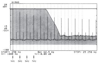
Figure A1 Frequency Domain (Spectrum Analyzer) Plot of 1kHz Square Wave (5VP-P) Input to LTC1064-1 as Configured in Figure 31.4. fCUTOFF = 10kHz. Shaded Area is the Frequency Response of the Filter
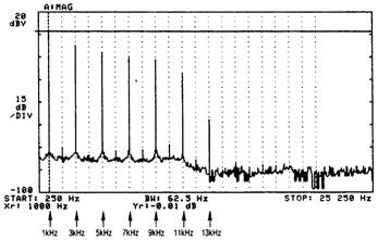
Figure A2 Filter Output (Shown in Frequency Domain) for 1kHz Input. Note Raised Noise Floor Due to LTC1064-1 Approx. 75dB Noise Level

Figure A3 Filter Time Domain Output for Input 1kHz Square Wave (Photograph Reproduction of Original)
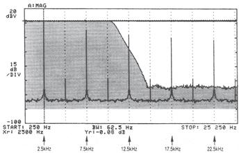
Figure A4 Frequency Domain (Spectrum Analyzer) Plot of 2500Hz Square Wave (5VP-P) Input to LTC1064-1 as Configured in Figure 31.4. fCUTOFF = 10kHz. Shaded Area is the Frequency Response of the Filter

Figure A5 Filter Output (Shown in Frequency Domain) for 2500Hz Input. Note Raised Noise Floor Due to LTC1064-1 Approx. 75dB Noise Level

Figure A6 Filter Time Domain Output for Input 2500Hz Square Wave (Photograph Reproduction of Original)

Figure A7 Frequency Domain (Spectrum Analyzer) Plot of 5kHz Square Wave (5VP-P) Input to LTC1064-1 as Configured in Figure 31.4. fCUTOFF = 10kHz. Shaded Area is the Frequency Response of the Filter

Figure A8 Filter Output (Shown in Frequency Domain) for 5kHz Input. Note Raised Noise Floor Due to LTC1064-1 Approx. 75dB Noise Level
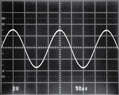
Figure A9 Filter Time Domain Output for Input 5kHz Square Wave (Photograph Reproduction of Original)
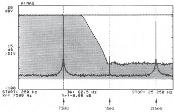
Figure A10 Frequency Domain (Spectrum Analyzer) Plot of 7500Hz Square Wave (5VP-P) Input to LTC1064-1 as Configured in Figure 31.4. fCUTOFF = 10kHz. Shaded Area is the Frequency Response of the Filter

Figure A11 Filter Output (Shown in Frequency Domain) for 7500Hz Input. Note Raised Noise Floor to LTC1064-1 Approx, 75dB Noise Level
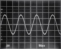
Figure A12 Filter Time Domain Output for Input 7.5kHz Square Wave (Photograph Reproduction of Original)
The series of figures illustrates a varied input square wave (from 1kHz to 7500Hz) to an LTC1064-1 Elliptic filter. Recall that a square wave consists of odd harmonics of the fundamental; that is, a 1kHz square wave should contain (in the mathematical work) 1kHz, 3kHz, 5kHz, 7kHz, 9kHz, 11kHz… spectral lines, that is sine waves, all added together to produce the 1kHz square wave.
Figures A2 and A3 show the Elliptic filter passing the 1kHz square wave with poor fidelity. As the input frequency increases, the fidelity decreases as fewer and fewer of the square waves’ spectral lines are passed through the filter.
Figures A5 and A6 show the spectrum analyzer and oscilloscope response from the filter’s output for an input square wave of 2.5kHz.
Figures A8 and A9 show the frequency and time domain responses from the filter’s output for an input square wave of 5kHz. The 10kHz cutoff frequency of the filter passes only the first harmonic (5kHz) and the 10kHz second harmonic (which is a signal generator problem and should not be there at all). The output appears to be a nice clean sine wave as seen in Figure A9.
Figure A10 shows the input spectrum of a 7.5kHz square wave. Figure A11 is the output from the filter in the frequency domain. In addition to the 7.5kHz spectral line producing the sine wave shown in Figure A12, there are other lines. These lines at 2.5, 5, 10 and 12.5kHz are the result of the 132nd, 133rd, 134th and 135th (!!!!!!) harmonics of the 7.5kHz fundamental frequency of the input square wave aliasing back into the passband of the filter. The perfect square wave should not contain even harmonics but the 133rd and 135th harmonic would remain. Again, WARNING: Bandlimit your input signal or risk aliasing!!1
Appendix B
About bypass capacitors
Bypass capacitors are used to maintain low power supply impedance at the point of load. Parasitic resistance and inductance in supply lines mean that the power supply impedance can be quite high. As frequency goes up, the inductive parasitic becomes particularly troublesome. Even if these parasitic terms did not exist, or if local regulation is used, bypassing is still necessary because no power supply or regulator has zero output impedance at 100MHz. What type of bypass capacitor to use is determined by the application, frequency domain of the circuit, cost, board space and many other considerations. Some useful generalizations can be made.
All capacitors contain parasitic terms, some of which appear in Figure B1. In bypass applications, leakage and dielectric absorption are 2nd order terms but series R and L are not. These latter terms limit the capacitor’s ability to damp transients and maintain low supply impedance. Bypass capacitors must often be large values so they can absorb long transients, necessitating electrolytic types which have large series R and L.

Figure B1 Parasitic Terms of a Capacitor
Different types of electrolytics and electrolytic-non-polar combinations have markedly different characteristics. Which type(s) to use is a matter of passionate debate in some circles and the test circuit (Figure B2) and accompanying photos are useful. The photos show the response of five bypassing methods to the transient generated by the test circuit. Figure B3 shows an unbypassed line which sags and ripples badly at large amplitudes. Figure B4 uses an aluminum 10μF electrolytic to considerably cut the disturbance, but there is still plenty of potential trouble. A tantalum 10μF unit offers cleaner response in B5 and the 10μF aluminum combined with a 0.01 μF ceramic type is even better in B6. Combining electrolytics with non-polarized capacitors is a popular way to get good response but beware of picking the wrong duo. The right (wrong) combination of supply line parasitics and paralleled dissimilar capacitors can produce a resonant, ringing response, as in B7. Caveat!

Figure B2 Bypass Capacitor Test Circuit

Figure B3 Response of Unbypassed Line

Figure B4 Response of 10μF Aluminum Capacitor

Figure B5 Response of 10μF Tantalum Capacitor
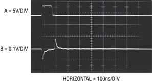
Figure B6 Response of 10μF Aluminum Paralleled by 0.01μF Ceramic
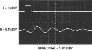
Figure B7 Some Paralleled Combinations Can Ring. Try Before Specifying!
Thanks to Nello Sevastopoulos, Philip Karantzalis and Kevin Vasconcelos for their generous assistance with this Application Note. Thanks to Lew Cronis for the inspiration to do Appendix A.
Bibliography
1. Sevastopoulos, Nello, and Markell, Richard, “Four-Section Switched-Cap Filter Chips Take on Discretes.” Electronic Products, September 1, 1988.
2. Brokaw, A. Paul, “An IC Amplifier User’s Guide to Decoupling, Grounding, and Making Things Go Right for a Change.” Analog Devices Data-Acquisition Databook 1984, Volume I, Pgs. 20-13 to 20-20.
3. Morrison, Ralph, “Grounding and Shielding Techniques in Instrumentation.” Second Edition, New York, NY: John Wiley and Sons, Inc., 1977.
4. Motchenbacher, C. D., and Fitchen, F. C., “Low-Noise Electronic Design.” New York, NY: John Wiley and Sons, Inc., 1973.
5. Rich, Alan, “Shielding and Guarding.” Analog Dialogue, 17, No. 1 (1983), 8-13. Also published as an Application Note in Analog Devices Data-Acquisition Databook 1984, Volume I, Pgs. 20-85 to 20-90.
6. Rich, Alan, “Understanding Interference-Type Noise.” Analog Dialogue, 16, No. 3 (1982), 16-19. Also published as an Application Note in Analog Devices Data- Acquisition Databook 1984, Volume I, Pgs. 20-81 to 20-84.
7. Williams, Jim, and Huffman, Brian, “Some Thoughts on DC-DC Converters,” Linear Technology AN29.
8. Jung, Walter, “IC Op Amp Cookbook.” Howard W. Sams, 1988.
9. Schwartz, Mischa, “Information, Transmission, Modulation and Noise.” New York, NY: McGraw Hill Book Co., 1980.
10. Zverev, “Handbook of Filter Synthesis.” New York, NY: John Wiley and Son, Inc., Copyright 1967.
11. Daryanani, Gobind, “Principles of Active Network Synthesis and Design.” New York, NY: John Wiley and Sons, Inc., Copyright 1976.
12. Ghausi, M. S., and K. R. Laker, “Modern Filter Design, Active RC and Switched Capacitor.” Englewood Cliffs, New Jersey: Prentice-Hall, Inc., 1981.
*From Anatol I. Zverev, “Handbook of Filter Synthesis,” Copyright © 1967 John Wiley and Sons, Inc., Reprinted by permission of John Wiley and Sons, Inc.
Note 1Sevastopoulos, Nello and Markell, Richard, “Four-Section Switched-Cap Filter Chips Take on Discretes.” Electronic Products, September 1, 1988.
Note 2Brokaw, A. Paul, “An IC Amplifier User’s Guide to Decoupling, Grounding, and Making Things Go Right for a Change.” Analog Devices Data-Acquisition Databook 1984, Volume I, Pgs. 20-13 to 20-20.
Note 3Morrison, Ralph, “Grounding and Shielding Techniques in Instrumentation.” Second Edition, New York, NY: John Wiley and Sons, Inc., 1977.
Note 4Motchenbacher, C.D., and Fitchen, F.C., “Low-Noise Electronic Design.” New York, NY: John Wiley and Sons, Inc., 1973.
Note 5Rich, Alan, “Shielding and Guarding.” Analog Dialogue, 17, No. 1 (1983), 8-13. Also published as an Application Note in Analog Devices Data-Acquisition Databook 1984, Volume I, Pgs. 20-85 to 20-90.
Note 6Rich, Alan, “Understanding Interference-Type Noise.” Analog Dialogue, 16, No. 3 (1982), 16–19. Also published as an Application Note in Analog Devices Data-Acquisition Databook 1984, Volume I, Pgs. 20-81 to 20-84.
Note 7Williams, Jim, and Huffman, Brian, “Some Thoughts on DC/DC Converters,” Linear Technology AN29.
Note 8Jung, Walter, “IC Op Amp Cookbook.” Howard W. Sams, 1988.
Note 9Schwartz, Mischa, “Information Transmission, Modulation and Noise.” New York, NY: McGraw Hill Book Co., 1980.
Note 10Zverev, “Handbook of Filter Synthesis.” New York, NY: John Wiley and Sons, Inc., Copyright 1967.
Note 11Daryanani, Gobind, “Principles of Active Network Synthesis and Design.” New York, NY: John Wiley and Sons, Inc., Copyright 1976.
Note 12Ghausi, M.S., and K.R. Laker, “Modern Filter Design, Active RC and Switched Capacitor.” Englewood Cliffs, New Jersey: Prentice-Hall, Inc., 1981.
Note 1Thanks to Lew Cronis for the inspiration to do this Appendix.