
Chapter 7. Transient Analysis
Chapter Outline
7.1. Simulation Settings101
7.2. Scheduling102
7.3. Check Points103
7.4. Defining a Time–Voltage Stimulus using Text Files104
Transient analysis calculates a circuit’s response over a period of time defined by the user. The accuracy of the transient analysis is dependent on the size of internal time steps, which together make up the complete simulation time known as the Run to time or Stop time. However, as mentioned in Chapter 2, a DC bias point analysis is performed first to establish the starting DC operating point for the circuit at time t=0s. The time is then incremented by one predetermined time step at which node voltages and current are calculated based on the initial calculated values at time t=0. For every time step, the node voltages and currents are calculated and compared to the previous time step DC solution. Only when the difference between two DC solutions falls within a specified tolerance (accuracy) will the analysis move on to the next internal time step. The time step is dynamically adjusted until a solution within tolerance is found.
For example, for slowly changing signals, the time step will increase without a significant reduction in the accuracy of the calculation, whereas for quickly changing signals, as in the case of a pulse waveform with a fast leading edge rise time, the time step will decrease to provide the required accuracy. The value for the maximum internal time step can be defined by the user.
If no solution is found, the analysis has failed to converge to a solution and will be reported as such. These convergence problems and solutions will be discussed in more detail in Chapter 8.
There are some circuits where a DC solution cannot be found, as in the case of oscillators. For these circuits, there is an option in the simulation profile to skip over the initial DC bias point analysis. If you add an initial condition to the circuit, the transient analysis will use the initial condition as its starting DC bias point.
7.1. Simulation Settings
Figure 7.1 shows the PSpice simulation profile for a transient (time domain) analysis. In this example, the simulation time has been set to 5μs. The Start saving data after: specifies the time after which data are collected to plot the resulting waveform in Probe in order to reduce the size of the data file.
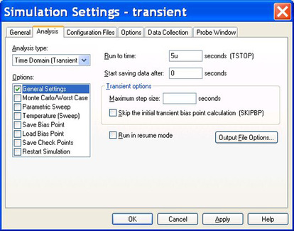
Maximum step size: defines the maximum internal step size, which is dependent on the specified run to time but is nominally set at the run to time divided by 50.
Skip the initial transient bias point calculation will disable the bias point calculation for a transient analysis.
7.2. Scheduling
Scheduling allows you to dynamically alter a simulation setting for a transient analysis; for example, you may want to use a smaller step size during periods that require greater accuracy and relax the accuracy for periods of less activity. Scheduling can also be applied to the simulation settings runtime parameters, RELTOL, ABSTOL, VNTOL, GMIN and ITL, which can be found in PSpice > Simulation Profile > Options. You replace the parameter value with the scheduling command, which is defined by:
{SCHEDULE(t1,v1,t2,v2…tn,tn)}
Note that t1 always starts from 0.
For example, it may be more efficient to reduce the relative accuracy of simulation from 0.001% to 0.1%, RELTOL, during periods of less activity by specifying a change in accuracy every millisecond. The format will be defined as:
{schedule(0,0, 1m,0.1, 2m,0.001, 3m,0.1, 4m,0.001)}
The simulation settings will be discussed in more detail in Chapter 8.
7.3. Check Points
Check points were introduced in version 16.2 to allow you to effectively mark and save the state of a transient simulation at a check point and to restart transient simulations from defined check points. This allows you to run simulations over selective periods. This is useful if you have convergence problems in that you can run the simulation from a defined check point marked in time before the simulation error, rather than having to run the whole simulation from the beginning.
Check points are only available for a transient simulation and are selected in the simulation profile in Analysis > Options box (Figure 7.2) as Save Check Points and Restart Simulation. Check points are defined by specifying the time interval between check points. The simulation time interval is measured in seconds and the real time interval is measured in minutes (default) or hours. The time points are the specific points when the check points were created.

Before you restart a simulation from a saved check point, you can change component values, parameter values, simulation setting options, check point restart and data save options. Figure 7.3 shows the Restart Simulation option selected.
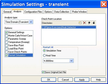
The saved check point data are set to simulation time in seconds such that Restart At shows 4ms, which was specified in the saved check point data file. The simulation will then start at 4ms using the saved state of the transient simulation.
7.4. Defining a Time–Voltage Stimulus using Text Files
The piecewise linear stimulus was introduced in Chapter 6, where a graphically drawn voltage waveform was used as an input waveform to a circuit. Input waveforms can also be defined using pairs of time–voltage coordinates, which can be entered in the Property Editor or read from an external text file.
Figure 7.4 shows the voltage VPWL and current IPWL sources and the corresponding time and voltage properties (Figure 7.5) in the Property Editor. By default, eight time–voltage pairs are displayed in the Property Editor for the VPWL and IPWL parts, but, as seen in Figure 7.5, more time–voltage pairs have been added. It is more efficient and easier to define a large number of time–voltage pairs in a text file.
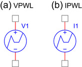
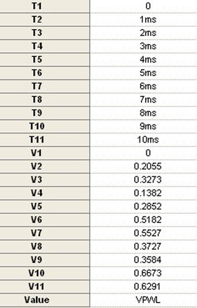
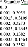
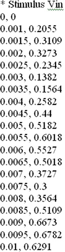
Figure 7.6 shows the VPWL_FILE part referencing a text file which contains time–voltage pairs as shown in Figure 7.7. For example, at 1ms the voltage is 0.2055V, at 2ms 0.3273V, and so on. It is always a good idea to make the first line a comment as PSpice normally ignores the first line.
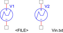
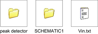
When you reference a text file such as Vin.txt, you need to specify the location of the text file. You can use absolute addressing specifying the direct path to the file or relative addressing specifying the path location relative to the project location. Figure 7.8 shows the hierarchy of a project showing the different folders in which the Vin.txt file can be placed and the corresponding <FILE> name for the referenced Vin.txt on the VPWL_FILE part.
For example, if you place the Vin.txt file in the same folder which contains the schematics, then you enter ..Vin.txt in the <FILE> property of the VPWL_FILE.
Project Folder > PSpiceFiles > schematics > simulation profiles
....Vin.txt ..Vin.txt Vin.txt
You can also provide an absolute path to a text file. For example, if you had a folder named stimulus, then you enter C:stimulusVin.txt.
In the source library there are other VPWL and IPWL parts which allow you to make a VPWL periodic for a number of cycles or repeat forever. These are given as:
VPWL_F_RE_FOREVER
VPWL_F_RE_N_TIMES
VPWL_RE_FOREVER
VPWL_RE_N_TIMES
IPWL_F_RE_FOREVER
IPWL_F_RE_N_TIMES
IPWL_RE_FOREVER
IPWL_RE_N_TIMES
The above source will be introduced in the exercises.
7.5. Exercises
Exercise 1
This exercise will demonstrate the effect that the maximum time step has on the resolution of a simulation and introduce the use of the scheduling command.
1. Draw the circuit in Figure 7.9, which consists of a VSIN source from the source library, connected to a load resistor R1.
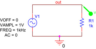
2. Create a PSpice simulation profile called transient and select Analysis type: to Time Domain (Transient) and enter a Run to time of 10ms, which will display 10 cycles of the sinewave (Figure 7.10).

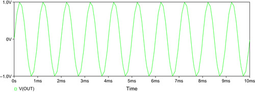
Place a voltage marker on node ‘out’ and run the simulation. You should see the resultant waveform as shown in Figure 7.11, which is lacking in resolution.
4. In the simulation profile, set up a schedule command to decrease the time step at set time points. You can enter the schedule command in the Maximum step size box, but because of the small field in which to type in the command it is recommended to type the schedule command in a text editor such as Notepad and cut and paste the following command into the box:
{schedule(0,0, 2m,0.05m, 4m,0.01m, 6m,0.005m, 8m,0.001m)}
5. Run the simulation. As the Mark Data Points is still on, you should see the resolution of the waveform improve with a decrease in the limit of the maximum step size (Figure 7.12).

Exercise 2
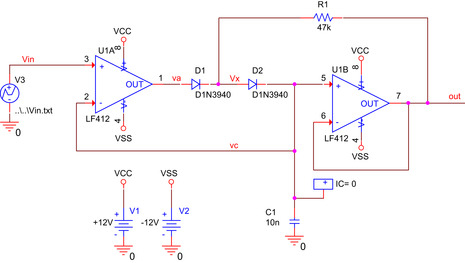
Figure 7.13 shows a peak detector circuit, where the input stimulus can be either the Vin Sourcstm source created in the Stimulus Editor exercise or a file containing a time–voltage definition of the input waveform. Both implementations will be described.
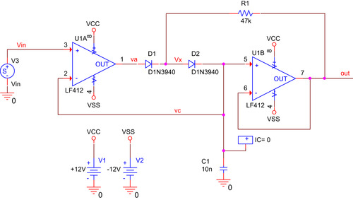
1. Create a project called Peak Detector and draw the circuit in Figure 7.13. If you are using the demo CD, use the uA741 opamps.
2. Rename the SCHEMATIC1 folder to Peak Detector.
3. You need to set up an initial condition (IC) on the capacitor, C1, by using an IC1 part from the special library. This ensures that at time t=0, the voltage on the capacitor is 0V  .
.
Alternatively, you can double click on the capacitor, C1, and in the Property Editor enter a value of 0 for the IC property value (Figure 7.14). This ensures that at time t=0, the voltage on the capacitor is 0V. If you change the capacitor, then you have to remember to set the initial condition, whereas an IC1 part will always be visible on the schematic.
4. Create a simulation profile, make sure you name it transient and set the run to time to 10ms. Close the simulation profile.
Two methods are described to define the input waveform Vin for the Peak Detector.
Using the Graphically Created Waveform in the Stimulus Editor
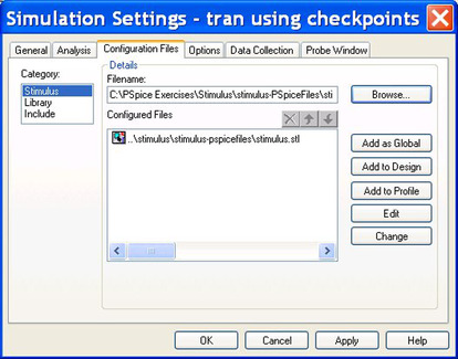
5. For the input stimulus, using the predefined Vin sourcestm in Chapter 6, edit the simulation profile and select the Configuration Files tab, select Category to Stimulus and Browse to the location of the stimulus.stl file. Click on Add to Design as shown in Figure 7.15. An explanation of stimulus files added to the simulation profile was given in Chapter 6.
6. Check the stimulus by highlighting the stimulus name and click on Edit. This will launch the Stimulus Editor and display the Vin waveform. Close the simulation profile.
7. Go to Step 12.
Using a File with Time–Voltage Data Describing the Input Waveform
8. Enter the time–voltage data points in Figure 7.16 in a text editor such as Notepad. By default, the simulator ignores the first line, so do not enter data on the first line. However, it is always a good idea to add a description or a comment to the data file using an asterisk ∗ character to describe, for example, what the data is. The simulator will ignore any lines beginning with a ∗ character.
Name the file Vin and save the file as a text file in the PSpice folder for the Project, Peak Detector > peak detector-PSpiceFiles (Figure 7.17).
9. Place a VPWL_FILE from the source library and rename the <FILE> shown in Figure 7.18 as ....Vin.txt

10. Your Peak Detector circuit will be as shown in Figure 7.19.
11. Go to Step 12.
12. Place voltage markers on nodes in and out and run the simulation.
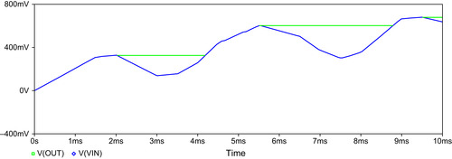
Figure 7.20 shows the simulation response of the peak detector to the input voltage Vin.
Generating a periodic Vin
13. Delete the VPWL_FILE source and replace it with a VPWL_F_RE_FOREVER from the source library. Double click on <FILE> and, as in Step 9, enter ....Vin.txt
14. Edit the PSpice Simulation Profile, increase the simulation run to time to 50ms and run the simulation. You should see the response as shown in Figure 7.21, where Vin is now periodic (repeats forever).

15. Investigate the VPWL_F_RE_N_TIMES source.
..................Content has been hidden....................
You can't read the all page of ebook, please click here login for view all page.