
Chapter 7: Building High-Performance Digital Circuits
This chapter presents the processes and techniques involved in assembling prototype high-performance digital circuits using surface-mount and through-hole electronic components. A recommended set of tools will be identified, including a soldering station, a magnifier or microscope, and tweezers for handling tiny parts. The reflow soldering process will also be introduced, along with descriptions of some low-cost options for implementing a small-scale reflow capability.
Preparations for circuit assembly and the techniques of soldering by hand and with the reflow process will be presented in a manner that allows them to be applied to a wide variety of projects. Once soldering is complete, the board must be cleaned and thoroughly inspected to ensure all intended connections are intact and that no unintended solder connections exist before applying power.
After completing this chapter, you will have learned how to assemble digital circuit boards. You will understand the tools and techniques required for circuit board assembly, as well as the steps involved in preparing for soldering. You will have learned how to solder surface-mount and through-hole components to the circuit board by hand and using a reflow system, and will also know how to clean the assembled board and thoroughly inspect it.
We will cover the following topics in this chapter:
- Circuit board assembly tools and procedures
- Preparing for assembly and placing parts
- Reflow soldering and hand soldering
- Post-assembly board cleaning and inspection
Let's get started!
Technical requirements
The files for this chapter are available at https://github.com/PacktPublishing/Architecting-High-Performance-Embedded-Systems.
Circuit board assembly tools and procedures
As a developer of a prototype digital device, you can construct a professional-looking, high-performance circuit board using surface-mount technology with a suitable set of tools and a bit of practice. This section will cover the needs of individual developers who are assembling a small number of circuit boards, typically one at a time. For manufacturers who need larger numbers of boards, ranging from dozens to hundreds or more, it is likely to be more appropriate, though more costly, to delegate this work to a company that specializes in PCB assembly.
Optical magnification
We will be assembling some very small components on the PCB. Many of the resistors and capacitors on our project circuit board use the 0402 package, with dimensions of 1.0 mm x 0.5 mm. To allow you to appreciate the size of these components, the following photo is of a resistor in the 0402 package size beside a grain of jasmine rice:

Figure 7.1 – Surface mount resistor beside a grain of rice
It may feel intimidating to work with such tiny components, but with a modicum of patience and practice, most people should be able to construct functioning circuit boards containing these components. Even if your eyesight is not the best, and if your hands shake a bit when you try to hold them perfectly still, such limitations can often be overcome.
The use of a magnifier or microscope allows you to get a view that is as close up as you desire, though you should not overdo it by using too much magnification. While many developers with reasonably good eyesight are happy to assemble PCBs with an inexpensive magnifying lens on a hands-free mount, or with no magnification at all, for small-component circuit assembly, I prefer to use a stereo microscope set at a low magnification. An example of this type of microscope can be seen in the following figure:
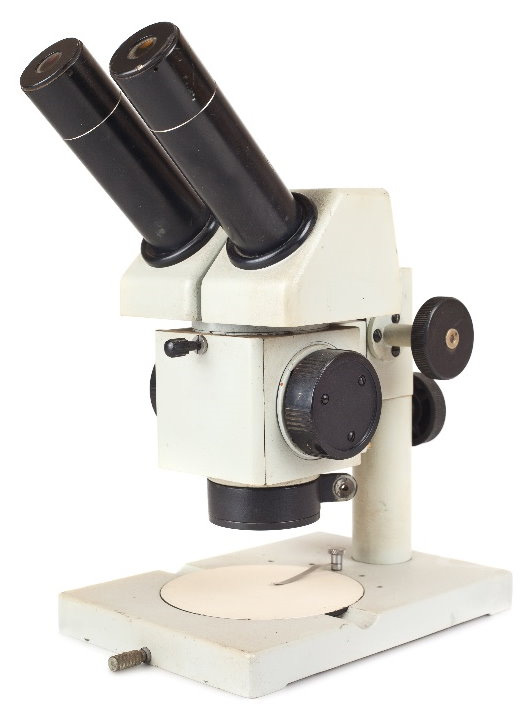
Figure 7.2 – Stereo microscope suitable for SMT soldering
When using a microscope, you should adjust the magnification to a level that allows a clear view of components the size of the resistor shown in Figure 7.1, while at the same time providing a sufficiently wide field of view of the surrounding board real estate. This allows you to remain oriented to the location on the PCB as you bring components in for placement using tweezers.
Any shaking that may occur when you're using tweezers can be reduced by providing a stable place to rest your hand while you're placing components. This hand rest can be constructed from books, bean bags, or other items that provide a comfortable and solid surface for your hand. Some circuit builders find it helpful to hold their tweezer hand with the other hand while placing smaller components.
It is not critical to place components at the exact location with perfect alignment on the first attempt. Placing the part in roughly the correct location is good enough initially. The part can then be moved and rotated by nudging it with tweezers or other appropriate small tools. Even when hand soldering, it is not necessary for the components to be in perfect alignment. It is good enough if you can solidly solder each of the connection points on the component to the board while avoiding problems such as solder bridges, which are unintended connections between signals on a PCB. Solder bridges are generally caused by applying too much solder when making connections. We'll learn how to fix solder bridges later in this chapter.
Tweezers
You need at least one good pair of precision tweezers for placing components on the circuit board and, when hand soldering, holding components in place while soldering the first connection. You should be able to find a precision tweezers set for a few dollars that includes a variety of tip orientations. The following photo is of a suitable pair of tweezers for electronic assembly:

Figure 7.3 – Tweezers suitable for electronic assembly
A pair of tweezers with a tip curved about 30°–45° from the body works well when placing components under a microscope. The angle of the tip allows you to place components straight downward while keeping your hand off to the side, away from the microscope hardware and out of your line of sight.
Flux
Oxidation is the enemy of good solder joints. Oxidation is a chemical process similar to the rusting of iron in that it produces a layer of poorly conductive material on a soldering iron or circuit component. When soldering, it is important to take a few steps to prevent oxidation from forming and degrading the quality of your solder joints. Fortunately, this is easy to do.
To prevent issues related to oxidation during soldering, it is important to keep the soldering iron tip clean, as described later in this section, and to use flux properly during soldering. Flux is a chemical compound that is nonconductive and inert at room temperature. When heated during soldering, flux performs three functions:
- It cleans oxidized deposits from the metal surfaces being soldered.
- It forms a protective barrier, preventing air from reaching the melted solder and the surfaces being soldered and causing oxidation.
- It performs a wetting function, allowing the liquid solder to flow freely over the metal surfaces. Wetting refers to the flow of liquid solder to all parts of a joint.
If you were to try soldering SMT components with no flux at all, you would find it very difficult to get a solid connection between the component and the board. This is due both to the difficulty of getting the solder to bond to the oxidized metal surfaces and to the poor flow characteristics of melted solder in the absence of flux.
Some types of solder wire have a hollow core filled with flux. When using this type of solder, it is important to ensure you use the soldering iron to heat the component and the PCB, then apply the solder to the heated metal until it melts and forms a joint. If, instead, you melt a glob of solder onto the tip of the iron and then attempt to form a joint, you will observe smoke drifting away as soon as the solder is on the tip. This is the flux burning off. If you use this approach, you convert flux-core solder into fluxless solder that is incapable of forming a good joint.
As an alternative to flux-core solder, it is possible to apply flux to the PCB with a felt-tip flux pen or directly as a liquid from a bottle. When soldering a PCB that has a pre-applied flux coating, you will find it is easy to produce good-quality joints. It does not hurt to have too much flux on the board, and too much flux is far better than having too little.
Some types of flux remain corrosive after soldering is complete and must be removed by a cleaning process. Another category of flux is called no clean, meaning the flux residue can be left in place once assembly is complete. Flux residue can be visually unappealing and sticky. Fortunately, it is easy to remove leftover flux, as we will see later in this chapter.
Solder
Solder for electronic assembly comes in two general types: tin/lead and lead-free. The tin/lead variant, which is commonly used for electronic assembly, is 63% tin and 37% lead by weight and has a melting point of 361°F (183°C). The nice features of tin/lead solder include its relatively low melting temperature and the ease with which you can produce high-quality solder joints. Its not-so-nice attribute is that lead is poisonous, even in small quantities.
It is possible to work safely with lead solder, as long as you set up an appropriate work environment and use reasonable care when soldering and cleaning up afterward. When working with solder containing lead, you should avoid inhaling fumes during soldering and wash your hands thoroughly after handling the solder.
You can avoid inhaling fumes during soldering with the assistance of a fume extractor or a fan. A fume extractor has an inlet that must be placed near the soldering area to suck in air, pulling the smoke produced during soldering into the device. The smoky air passes through a filter that absorbs the smoke residue before passing the clean air back into the room or outside via an exhaust system. A fan, on the other hand, simply blows the smoke around the room. Clearly, a fume extractor is better because it removes the smoke residue, rather than just spreading it around, though an extractor will generally cost more than a fan. A fan is better than nothing, because it will at least prevent the smoke from rising directly into your face.
Lead-free solder is available in a few different formulations. One readily available formula used in electronic assembly is 99.3% tin and 0.7% copper. This tin/copper alloy has a melting point of 441°F (227°C), significantly higher than the melting point of tin/lead solder, making lead-free solder somewhat more difficult to work with. The higher melting point of lead-free solder may also produce a greater quantity of flux fumes due to the higher soldering temperature. Even though lead-free solder avoids the hazard of lead poisoning, it is still unhealthy to inhale the fumes it gives off. Proper ventilation is essential for soldering in all cases. If you are manufacturing an electronic product for commercial sale, the use of lead-free solder may be mandatory.
When selecting solder wire, it is important to select an appropriate thickness. Because we are working with very small SMT components, it is necessary to use thin solder wire. If the wire is too thick, it becomes very difficult to melt an appropriate quantity of solder at the desired location. For the sizes of the components we will be soldering, the solder wire thickness should be no greater than 0.032" (0.81 mm). I prefer to use 0.020" (0.51 mm) rosin core solder for hand soldering SMT components. Rosin is a particular type of flux made from tree sap that is commonly available in hollow core solder wire. The following photo is of a spool of 0.020" rosin core solder:
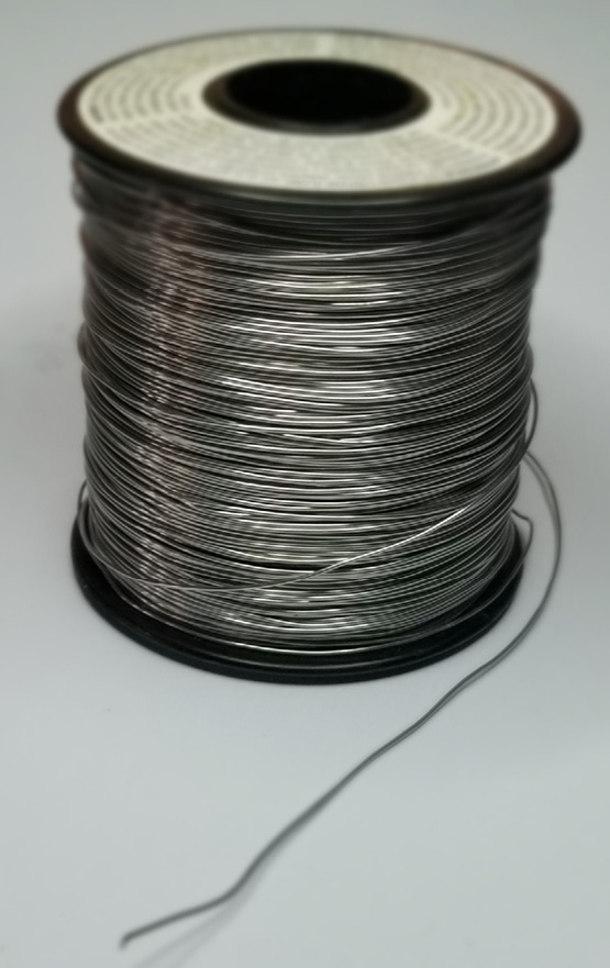
Figure 7.4 – Spool of 0.020" rosin core solder wire
When using solder wire, it is best to pull about 1 foot of wire from the spool and use the heated tip of the soldering iron to cut the wire segment from the spool. The piece of wire can then be used to perform delicate soldering until it has been reduced to a length too short to hold easily for further soldering. Be sure to handle unused solder wire and soldered items as hazardous waste and dispose of them appropriately.
Electrostatic discharge protection
Many of the integrated circuits and other electronic components we will be assembling are sensitive to electrostatic discharge (ESD). ESD occurs when two electrically charged bodies either come into contact or move close enough together that a spark can jump the gap between them. When this happens, a large electrical current can flow for a very brief period of time, damaging or destroying sensitive electronic components.
Because ESD is so potentially harmful to the success of your circuit construction project, it is worth taking precautions to prevent it from causing problems. You can take a few steps to minimize the risk of ESD damage to components while assembling circuits.
The general goal of ESD protection during circuit assembly is to prevent the buildup of electrical charge on you and on the items you're working with during circuit assembly. Follow these steps to reduce the risk of harmful ESD:
- The first step in ESD protection is to use an ESD-safe mat as your work surface. An ESD mat has a high electrical resistance, but it is not an insulator. By connecting the ESD mat to electrical ground (which is available at the center screw on standard electrical power outlets), you can ensure that any electrical charge on the components and tools you are working with will dissipate when those items are placed on the mat. ESD mats are widely available at reasonable prices.
- The second step in ESD protection is to prevent electrical charge from building up on your body. An ESD wristband with a wire connected to ground will dissipate charge from your body and prevent you from zapping components when you touch them.
If your work area has synthetic carpeting or another floor covering associated with electrostatic charge buildup, you can put down an ESD-safe floor mat to reduce charge buildup as you move about the area.
When you receive electronic parts you have ordered, you will see they arrive in ESD-safe protective packaging. It is critical to only open the packaging and remove the components in an ESD-safe environment while you are wearing a grounded wrist strap. It is generally best to leave all the components inside their packaging until you are ready to assemble them on to the board.
Hand soldering
We will cover two basic approaches for constructing prototype circuit boards: hand soldering and reflow soldering. This section will discuss hand soldering; reflow soldering will be covered in a later section. As you will see, reflow soldering is the preferred approach when working with large numbers of SMT components. Although we will recommend the use of reflow soldering where possible, in most circuit projects, there is also a need for some hand soldering to add components such as connectors for power and communication paths to external components. Hand soldering is also the way we repair any problems that arise with component placement and connections during reflow soldering. If you lack the tools necessary for reflow soldering, hand soldering is available as an alternative.
Hand soldering involves the use of a handheld soldering iron and other handheld tools, including a hot air gun, solder, and tweezers. For the work we will be doing, it is best to use a soldering station that combines a handheld soldering iron with a handheld hot air gun. This type of soldering station is often called a rework station, which refers to a station that can be used to disassemble and repair circuit boards, in addition to performing circuit assembly. The following is an example of a rework station:

Figure 7.5 – Solder station with an iron and hot air gun
The rework station shown in the preceding figure provides digital displays of the temperature of the soldering iron and the hot air gun. An additional control is provided to adjust the airflow through the hot air gun. Most soldering stations of this type include a variety of tip shape options for the soldering iron and a selection of nozzle shapes and sizes for the hot air gun. Because we are working with very small components, the best tip for the soldering iron is most likely to be the tip that comes to the smallest point. This enables heat transfer to the precise location where it is desired without heating, and possibly damaging, other parts of the circuit.
Accurate temperature control is critical when soldering surface mount components. The least expensive soldering irons do not provide a mechanism for monitoring or adjusting temperature, so they should be avoided when performing PCB assembly.
As a starting point, a soldering iron temperature that's 30–50°F (20–30°C) above the melting point of the type of solder you are using is suitable for soldering small components. As your skill level increases, you can increase the temperature to melt the solder faster. With higher temperatures, you will need to complete the joint and remove the iron quickly to avoid overheating and damaging the component.
When soldering, you should make frequent use of the tip cleaning pad, which is usually a sponge or a clump of coiled wire. If a sponge is available, as is the case with the solder station shown in the preceding figure, it must be kept wet; otherwise, the hot iron will burn it. The sponge should be fairly damp but not saturated with water. To clean the solder iron tip using the sponge, the iron must be fully heated. Wipe the tip across the sponge while twisting the iron to clean the full circumference of the tip. If you're using a wire coil tip cleaner, insert the hot iron tip into the coil a few times to give the wires a chance to scrape off any excess solder and oxidation.
The solder station hot air gun is useful for heating a larger area in comparison to a soldering iron. This area-heating capability can melt solder on multiple pads simultaneously, such as when removing an SMT integrated circuit from a board. Hot air can also be used to solder integrated circuits onto the board.
Some IC package types are not suitable for soldering with a soldering iron and, if a reflow soldering process is unavailable, can only be soldered using hot air. For these components, a generalized procedure is to apply a light coat of flux to the board, then use a soldering iron to apply a thin layer of solder to the pads (this is called tinning), before placing the IC on the pads and using hot air to solder all of the pads simultaneously. When using hot air to solder components in this manner, it is important to avoid blowing the part off-center and to avoid inadvertently desoldering and blowing away any surrounding components. For this reason, any components that must be soldered using hot air should be installed on the PCB first.
Solder wick
Sooner or later, when hand soldering, you will accidentally apply too much solder to a joint and end up with a solder bridge between pins on an IC or between closely spaced components. It is straightforward to remove excess solder using solder wick. Solder wick is braided copper wire intended to absorb melted solder. Just like when you're assembling components, removing excess solder works best when there is flux present on the wick and on the area containing the excess solder.
To use solder wick, first ensure there is flux present on the wick and on the area containing the excess solder. Place the clean, unused end of the wick on the excess solder, then press down on the wick with the hot soldering iron. It may take a few seconds, but, eventually, the solder will melt and flow into the wick. Once the solder has been absorbed, remove the wick and the soldering iron from the board simultaneously. If you remove the iron first, the melted solder will harden, and the wick will remain stuck to the board.
The following is an example of solder wick after being used to remove some solder:
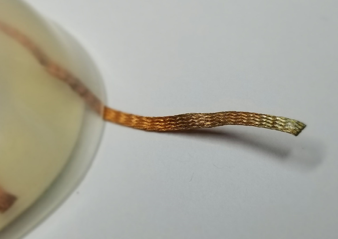
Figure 7.6 – Solder wick containing removed solder
After using solder wick, clip off the section of wick containing the removed solder. This leaves a clean end for its next use.
Solder paste application
Reflow soldering uses solder paste, which is a mixture of sticky flux and microscopic balls of solder, to loosely attach a potentially large number of circuit components to their pad locations on a PCB. Once all the components have been placed onto their solder paste-covered pads, the entire PCB assembly is subjected to a heating profile that melts the solder, forming a solder joint at each pad location. The term reflow soldering refers to the fact that each time the solder temperature is raised above its melting point, it becomes liquid, with the corresponding ability to flow.
For the developer of a prototype circuit board, one obvious advantage of reflow soldering compared to hand soldering is that you don't need to solder every connection point between the components and the PCB. Instead, it is necessary to apply solder paste to the component pads and place the components accurately before heating the board.
One approach is to apply solder paste manually, using a syringe to dispense the material onto individual pads. It is also possible to use a stencil containing appropriately sized holes at each PCB pad location to apply solder paste to all the pads on the PCB in a single operation. Solder paste stencils are constructed using the data files produced during the PCB layout process, as discussed in the Prototyping the circuit board section of Chapter 6, Designing Circuits with KiCad.
To apply solder paste to a PCB using a stencil, it is helpful to prepare a frame that will hold the stencil in place on top of the PCB, as shown in the following figure. The frame helps ensure the holes in the stencil remain in position over the PCB pads and that when you're lifting the stencil away, the movement is straight upward rather than sideways, which may smear the solder paste. You should be able to purchase a frame when you buy the stencil, though you can make one yourself from suitable material such as unpopulated circuit boards:

Figure 7.7 – Solder stencil attached to a frame
It is best to use solder paste purchased in a jar for working with solder stencils. By utilizing this approach, you will apply much more solder paste to your spreader than you actually need to fill in the holes in the stencil. Once stenciling is complete, you can scrape the excess paste from the stencil and put it back in the jar for later use. If, instead, you dispense the paste from a syringe, you will most likely discard any excess paste.
For spreading the paste onto the stencil, you will need a tool with a straight, flexible edge. Depending on the size of your circuit board, this tool might be anything from a credit card, to a putty knife, to a large drywall taping knife. For our project circuit board, the free credit card-sized paste spreader provided by OSH Stencils with each stencil purchase will serve our needs.
Applying the solder paste to the stencil atop the PCB in the frame can be done quickly, but it requires a bit of finesse. In particular, if you find you have missed areas of the stencil holes on the first pass, or if the application is otherwise uneven, repeated attempts to apply the paste may result in excessive buildup of solder paste under the stencil – in other words, a mess. Don't be discouraged if you need to clean off the PCB and the stencil after your first attempt and start over. You can clean the solder paste from the stencil and from the board using isopropyl alcohol (IPA) and a lint-free cloth.
To apply the solder paste to the stencil, perform the following steps:
- Ensure the PCB, the frame, and the stencil are lying perfectly flat on a hard surface. The frame should be the same thickness as the PCB, and the holes in the stencil must be carefully aligned with the PCB pads. You can use removable tape such as painter's masking tape to hold the stencil in position.
- The spreader must be wide enough to cover all the holes in the PCB while passing in a straight line across the surface.
- Open the jar of solder paste and stir the paste thoroughly with a tool, such as a small screwdriver.
- Use the stirring tool to load a bead of solder paste on one side of the spreader, along the straight edge.
- Place the spreader on the stencil, with the side holding the solder paste facing toward the area to be stenciled.
- Tilt the top of the spreader about 45° in the direction it will be moving.
- In one smooth sweep, with continuous downward pressure, move the spreader across all the stencil holes. This should completely fill the holes with paste.
- Turn the spreader around and prepare to make a sweep in the opposite direction. The purpose of this sweep is to scrape off the solder paste residue from the stencil's surface.
- Tilt the spreader so that it's nearly vertical, and leaning slightly in the direction of motion. Make another smooth sweep in the opposite direction of the first sweep.
- Scrape the solder paste residue from the spreader into the jar and seal the jar.
- Carefully lift the stencil from the PCB.
- Examine the PCB and verify that all the pads that should have received solder through the stencil have received it. Not all the pads should receive solder paste. Some, such as those for through-hole connectors, are not intended to be soldered during this process.
If all has gone well, you should now have a PCB with appropriate quantities of solder paste applied to all the SMT component pad locations. Feel free to congratulate yourself on this success, but be aware that by completing this step, you have started a ticking clock.
Solder paste has a stickiness, referred to as tack, that holds components in place once they have been positioned. Once the paste is exposed to the air, some of its chemical components begin to evaporate, reducing its stickiness. As a general rule of thumb, you should plan to wait no more than 8 hours between stenciling solder paste onto a board and completing the reflow process. In other words, you should not plan to wait overnight once you've stenciled a board before you populate it and perform the reflow.
Applying solder paste transforms the PCB into an extremely delicate item that can be easily disturbed. You must be exceptionally careful when handling the stenciled PCB and while placing components on it to ensure you do not brush against any of the paste-covered pads, as this will wipe the paste away, along with any components you may have already placed at those locations. Even the lightest contact between your hand or tweezers and the paste may have drastic consequences.
When placing components on the solder paste-covered pads, it is best to work from the center of the board outward. Whether you use a magnifier, a microscope, or no magnification at all, you must be very careful to avoid contact with the board at any point other than the target placement location for each component. As you continue populating the PCB, rotate the board so that you do not have to reach across to the far side to place any of the components.
Reflow soldering
Once all the components have been placed, the board is ready for reflow soldering. The reflow process is standardized across the industry for SMT boards and circuit components. In factories, large quantities of PCBs are soldered in succession in large reflow ovens that transport the boards through areas of varying temperature based on the intended heating profile.
For hobbyists and other small-scale prototype PCB developers, it is not practical to employ the processes and equipment used in electronic device factories for building one board at a time. The essential functionality of the reflow process equipment is to heat the PCB and the solder paste it carries to a temperature that allows the solder to melt and reflow, while avoiding problems such as overheated and damaged circuit components.
A typical reflow temperature profile can be seen in the following diagram. The profile contains four major phases: preheat, soak, reflow, and cooldown:

Figure 7.8 – Reflow soldering temperature profile
The purpose of each of these phases is as follows:
- Preheat: In this phase, the board is quickly brought to the soak temperature and the flux solvents begin evaporating.
- Soak: In the soak phase, the flux solvents finish evaporating, and the flux removes oxides from the surfaces to be soldered. Larger circuit components have time to approach the soak temperature, which will minimize thermal stress during the reflow phase.
- Reflow: The temperature increases above the liquidus temperature (TL), which is the melting temperature of the solder. The temperature remains above TL for 1–2 minutes to allow sufficient time for all the solder on the board to reflow.
- Cooldown: The cooldown phase returns the board to room temperature fairly quickly. A quick cooldown is desirable both for the purpose of minimizing process time and to produce stronger solder joints compared to those resulting from a slower cooling phase.
The reflow process takes about 10 to 15 minutes from beginning to end. The reflow heating profile described here represents an ideal process typically performed using sophisticated manufacturing equipment. Developers on a tight budget have developed procedures for performing reflow soldering using kitchen appliances, such as an electric hot plate and a skillet, or with a toaster oven, with varying results.
At the lowest level of sophistication, a developer can set a PCB with placed components on a skillet positioned on a hot plate and turn on the heat. By watching the solder paste closely as the board heats, you can determine when the solder has melted and remove the board from the heat. While some developers claim this technique produces consistently successful results, it is not a well-controlled process.
Other developers have used toaster ovens to perform reflow soldering with temperature indicator material. Temperature indicators allow you to place markings on a PCB that change color when the target temperature is reached. The toaster oven method relies on watching for the indicator to change color through the window of the oven door and removing the board from the heat when the appropriate temperature has been reached.
Various modifications for standard hot plates and toaster ovens to improve their reflow processing capabilities have been developed by talented individuals who retrofit these devices with temperature monitoring and control systems. These modified kitchen appliances are capable of implementing temperature profiles similar to the one shown in the preceding diagram. An internet search for phrases such as toaster oven reflow or hot plate reflow will provide you with more information about these efforts.
You can build your own modified hot plate or toaster oven, or you can even purchase a small, dedicated reflow oven for under $300 from a variety of sources. If you use a toaster oven for reflow soldering, you must never use it to cook food. This is because the oven will become contaminated with flux residue and, if you use lead solder, lead residue as well.
Regardless of the type of reflow system you end up using, the goal is to create good connections at every solder joint on the board. The following photo shows some solder joints that have been produced in a low-cost dedicated reflow oven with hand-placed 0402 and 0603 capacitors using stencil-applied solder paste:
Figure 7.9 – Reflow soldered 0402 package capacitors
If you do not have a reflow oven available, the circuit board for the oscilloscope project can be hand-soldered, with the exception of the U1 and U8 integrated circuits. Both of these components require the back of the device to be connected to board ground, in addition to the pins around the chip perimeter. It may be possible to solder these devices using hot air, as described earlier in this chapter.
Before we move on, please review the following soldering safety recommendations.
Soldering safety tips
Be sure to keep these points in mind while soldering:
- Wear safety glasses when soldering. It is possible for hot solder to splatter if it comes into contact with moisture.
- Avoid letting the soldering iron, the hot air gun, or the air exiting the air gun come into contact with people, electrical cords, or anything else you don't want melted or burned.
- Ensure the soldering iron cleaning sponge is sufficiently wet before turning the iron on.
- Turn the soldering iron and hot air gun off immediately after you've finished using them.
- Remember that the iron and gun remain hot for some time after being turned off, and that the circuit boards and components are very hot immediately after being soldered.
- When you put down the soldering iron and hot air gun, be sure to place the tool in the appropriate holder. Do not lay a hot tool on your workspace surface.
- Use a fume extractor, or at least use a fan, to blow the fumes away from your face.
- Do not wear loose-fitting clothing or jewelry that might come into contact with the soldering iron or your circuit components.
- Wash your hands thoroughly with soap and water after handling lead solder.
- Do not reuse a toaster oven that has been used for reflow soldering to cook food.
- Ensure small children and pets cannot gain access to a work area containing hot tools and lead solder.
- Have a first aid kit available. You are likely to burn yourself at least once before you master the ability to handle a soldering iron safely.
The recommended approach for assembling the oscilloscope project circuit board is reflow soldering, using the heating system of your choice. The steps for preparing and assembling this board are provided in the next section.
Preparing for assembly and placing parts
When the time comes to assemble a circuit board, you should begin by confirming you have everything you need to finish the job. When you reach this point, you will have a bare circuit board plus all of the circuit components you will need, as well as the tools and consumables needed for applying solder paste and performing reflow soldering.
It is helpful to purchase extra circuit components in case you lose or damage any of them during assembly. This is an easy thing to do for inexpensive parts such as SMT resistors and capacitors. For more expensive components, typically integrated circuits, you will have to decide how many spares your budget can tolerate.
The task of placing a large number of components on a board can be quite tedious and error-prone. Your work area should be clear of any obstructions and distractions that might interfere with your ability to successfully populate the board.
It is critically important to ensure the correct component is placed at each location on the PCB. This may seem obvious, but because many SMT resistors and capacitors have no markings indicating their resistance or capacitance, if devices with different values get mixed together, the only way you can determine which is which is by measuring their resistance or capacitance. This is possible, but it is far better to avoid this type of problem in the first place. This work is hard enough already.
The PCB silkscreen layer shows the annotated number of each resistor or capacitor, but it does not identify the resistance or capacitance of the part. You can examine the circuit schematic diagram to identify the resistance or capacitance of each part, but this is not the easiest way to find component information as you are placing parts on the board.
KiCad can create a text file called the bill of materials (BOM) that lists the circuit components, along with their annotated reference numbers and label information indicating the resistance and capacitance values. This function is available in the Pcbnew application's File menu. Select Fabrication Outputs and then BOM File…. The resulting output file is in comma-separated values (CSV) format with semicolon separators. You can import this file into a spreadsheet application and use it as a guide as you place components. I find that the best way to do this is to print out a page with the BOM and cross off each component once it has been placed. This allows me to deviate from the sequential part number order and, for example, place all the 0.1 µF capacitors before moving on to a different component type.
Even with the BOM available on paper, it can still be challenging to quickly find where each component goes on the board. It is helpful to open the PCB layout in the Pcbnew application while placing the components. You can use the Find… function on the Edit menu, or just press Ctrl + F, and search for component identifiers. For example, typing r20 in the Search for dialog that Ctrl + F brings up will highlight and place the cursor on the R20 resistor on the board layout, showing you where to find the part on the board you are assembling.
The following checklist will help you prepare for board assembly:
- The PCB must be ready for assembly. Any undesired tabs or protrusions from the PCB manufacturing process must be removed and the board must be completely clean and dry.
- All circuit components are available and organized so that you can find them easily. This includes a sufficient quantity of resistors and capacitors of all values needed. ESD-sensitive devices should not be removed from their protective packaging until you are ready to place them. In this phase, we are only installing surface-mount components. Other board components, such as through-hole connectors, will be installed once reflow soldering is complete.
- A staging area is available to hold parts once you've removed them from their packaging. This area should be light-colored to make it easy for you to see the tiny components. A sheet of white printer paper works well for this purpose.
- A microscope or magnifier, if desired, should be in a location suitable for comfortable use. Precision tweezers must be available for placing components.
- The reflow oven or hot plate must be ready to use. You do not need to heat it up until the board is ready to bake.
- The solder stencil must be aligned with the PCB and ready to receive solder.
Once you've completed these steps, it is time to apply solder paste to the board. Follow the steps in the Solder paste application section earlier in this chapter to apply the paste and inspect the results.
As we mentioned earlier, there is something of a time limit once the solder paste has been applied. This does not mean you should rush the parts placement process. Feel free to take breaks as necessary to stay relaxed and focused on the task.
As a reminder, try to maintain constant awareness of the location of your hands and tools relative to the PCB any time you are near it. It is very easy to accidentally brush against the board and wipe away solder paste and previously placed components. If this happens, stop and take a moment to evaluate the situation. If the disruption is minor, you may be able to use tools to push the paste and components back onto the proper pads. If you've lost track of which component goes where, you may need to discard resistors and capacitors and replace them with new components.
If the damage is more severe, you can decide whether you want to continue populating the board or start over. If you have more than one board, you can apply solder paste to a second board and transfer the components from the first board to the second.
Alternatively, if a portion of the board is no longer suitable for parts placement but the rest is undamaged, you may want to finish placing parts on the undamaged area and perform reflow soldering. Once reflow soldering is complete, you can hand solder the remaining components to the board. Of course, maintaining sufficient care during parts placement avoids this issue in the first place.
Once you have finished placing all the parts, congratulate yourself and take a short break. Then, perform a visual inspection and verify that all the parts have been placed and that they are in the proper locations and orientations. In particular, for any part that has a single correct orientation, such as integrated circuits and polarized capacitors, verify that the part is aligned properly.
The board is now ready for reflow soldering. The reflow soldering procedure is the subject of the next section.
Reflow soldering and hand soldering
At this point, the PCB sits on your assembly workspace, fully populated with SMT components. Now, it is time to turn on your reflow oven or hot plate.
Reflow soldering
Regardless of what type of reflow system you use, exercise extreme care when moving the PCB from your workspace to the oven or hot plate. If you strike the board against an object or, worse, drop it, you are likely to find that all your hard work placing the components was done for naught.
Your level of involvement during reflow soldering depends greatly on the technical capabilities of your reflow system. If you are using a stock hot plate or toaster oven, it is entirely up to you to monitor the state of the PCB as the solder heats and melts. If you remove the board from the heat too soon, you will have areas of unmelted solder, which means electrical contact will be poor to nonexistent, and parts may fall off the board. If you wait too long to remove the board from the heat, you risk overheating and damaging the components on the board.
If you have an automated oven – either a dedicated reflow oven or a toaster oven modified with temperature monitoring and control capabilities – your job is much easier. With these ovens, you simply place the board in the oven and, conceptually at least, push a button to start the process. The oven will run through a heating profile similar to the one shown in Figure 7.8. At the end of the cooldown phase, the board will be at a temperature not too far above room temperature.
Once the board is cool enough to handle, it is time perform an inspection to verify that each component remained in its proper location and orientation during reflow, and that all the solder connections are smooth and shiny. You should examine locations where traces or pads are close together, such as closely spaced integrated circuit pads, for solder bridges. For IC packages that have pins reaching beneath the plastic case, it can be hard to visually determine whether the connections are good. Examine the joints from various angles to find the best view.
If you see instances of solder bridges, use solder wick to remove the excess solder. If any components are mysteriously missing or have shifted to an unsuitable orientation, or just do not appear to have a good solder connection, make note of them so that you can fix each problem during the hand soldering phase.
Hand soldering
The two objectives of the hand soldering process are to fix any problems that occurred during reflow soldering and to attach the remaining through-hole components to the PCB.
It is better to fix any problems from reflow soldering before moving on to installing the remaining board components. This is because it's easier to access the different parts of the board before the through-hole components have been installed.
Repairs after reflow
If any parts have shifted to inappropriate positions or orientations during reflow, this can be fixed with hand soldering. As always, flux should be used to improve the soldering results.
If a component has become raised or tilted, you may be able to fix it by pressing it down with tweezers or another sharp tool while you melt the solder with the iron. After doing this, ensure all the component pads have good connections. When resoldering the joints of smaller SMT resistors and capacitors, it should take just a second or two of contact with the hot iron to melt the solder.
You may need to remove some components before you can properly position them on the board. With smaller resistors and capacitors, especially if only one end is attached, you can melt the solder while lifting the part with tweezers. If a larger component, such as an integrated circuit, is in the wrong position, you will need to use hot air to remove it. Grasp the component with tweezers and attempt to lift it while simultaneously aiming the hot air directly downward on it. The intent of this operation is to release the target component from the board while you avoid melting the solder holding any of the surrounding components to the board. If that happens, the air from the gun is likely to blow the other components across the board.
When reattaching components that have been removed from the board, begin by placing a light coat of flux on the pads to be connected. Align the part and tack down one pad. Since flux is already on the pads, it is acceptable to place a small amount of solder on the tip of the iron and touch it against the part and the pad. A second or two of contact should be sufficient.
If the alignment of the reattached part looks good once the first pad has been tacked, rotate the board and tack a pad opposite from the first one. If there are additional pins, proceed with soldering each of them in the same fashion.
Installing through-hole components
Once any post-reflow repairs have been completed, it is time to solder the through-hole components to the PCB. For the oscilloscope project, this includes the BNC connector for the oscilloscope probe, the 2 x 6 pin board edge connectors that will plug into the Arty board Pmod connectors, the 2 x 3 pin connector for the SPI interface, and the four test point loops.
Compared to SMT soldering, attaching the through-hole components is less of a delicate exercise. If you have a soldering iron with a higher wattage than the iron used for SMT component soldering, you may want to use it. It may take several seconds for an iron with a fine-pointed tip to heat the component and the board to the point where the solder melts.
To attach each component to the board, first place it in position and, if necessary, use clips to hold it in place. If you use plastic clips, make sure the plastic doesn't come into contact with the metal part of the component you will be soldering first.
Start by soldering one pin of the component to the board. If you used a clip to hold it in place, remove the clip once the first pin has been soldered.
Examine the part to ensure it is properly oriented and aligned. If necessary, you can reheat the solder and realign the part. This is the advantage of soldering only one pin on the first pass.
With the part aligned properly, finish soldering the remaining pins. Take your time and ensure you use enough solder so that it fills the hole and flows through to the other side of the board. This creates a strong electrical and mechanical joint between the component and the board. This strength is critical for parts that will undergo physical stress during use, such as connectors.
The two larger posts under the BNC connector are the largest solder joints on the board. Be sure to take enough time to heat the post and use plenty of solder to fill in the pad on the back of the board.
If any of the through-hole components contain leads that protrude significantly from the back of the board, use a pair of flush-cutting diagonal cutters to trim the lead just above the solder joint.
Once all the through-hole components have been installed, take a look at the board again. Make sure all the components have been installed and oriented correctly. If everything looks good, you are ready to clean the board and perform the final inspection, prior to applying power.
Post-assembly board cleaning and inspection
It is best to clean excess flux from the board shortly after soldering is complete. If the flux has an opportunity to dry out, it can be difficult or impossible to remove the residue.
If your solder paste is of the no-clean variety, you may choose not to remove the residue. No-clean solder paste leaves behind a limited quantity of flux residue, and this material is non-corrosive. It may be more difficult to remove the residue of this type of flux than to remove rosin flux.
Rosin flux should be cleaned from the board after soldering. This includes work done with rosin core solder wire and with liquid or pen-applied flux. The reasons why cleaning is necessary are as follows:
- Flux residue is visually unappealing. Rosin flux residue is a clear, shiny material with a yellow color that users of the device will notice. Customers purchasing the product may raise concerns about the quality of construction if it is present.
- The residue is sticky. This is not just a problem for fingers touching the board. If a metallic object comes into contact with the sticky material, it may attach itself and produce a short circuit that damages the board.
- Flux residue makes inspection more difficult. If the residue covers solder joints, it can be hard to examine the quality of the work.
- Rosin flux residue is acidic. If not removed, the residue can lead to corrosion and eventual failure of the board.
In general, each time soldering is performed on a board using rosin flux, it is necessary to clean the board afterward. When you're reflow soldering with no-clean flux, cleaning the board is optional.
Flux removal
Cleaning flux from the board is a straightforward procedure. Although several methods can be used, including the use of a dedicated washing machine, a simple method is to use a toothbrush and 91% IPA.
A variety of flux cleaning chemicals are also available that may do a better job than IPA. For board prototyping purposes, removing enough flux to make the board look and feel clean is our objective. For commercial applications, particularly in situations where safety and long-term reliability are critical, more stringent cleaning procedures are appropriate.
When working with IPA and flux residue, you should wear rubber gloves and safety glasses. Be sure to work in a well-ventilated area. IPA is highly flammable, so avoid working around heat, flames, or any anything that can produce sparks.
Pour some IPA into a small, shallow dish and dip a stiff toothbrush into the liquid. Scrub the flux-coated areas of the board with a circular motion. In the first pass, ensure all the flux is covered with IPA. Let the board sit for a minute or so while the IPA dissolves the residue, then scrub again to remove the material. Repeat this process as needed until the board is clean.
When you are finished, use either compressed air to blow the remaining IPA from the board, or use a paper wipe to dry the board. Inspect the board to determine whether all the visible flux has been removed. If necessary, repeat the flux removal process to clean the remaining areas.
This cleaning method will obviously not remove flux beneath components and between closely spaced IC pins. For our purposes, we will not concern ourselves with the small quantity of flux remaining in these areas.
Post-assembly visual inspection
Once the board has been assembled and cleaned, it is time to perform a final detailed inspection. With the flux residue removed, it will be easier to closely examine each solder joint and identify whether any repairs are needed. The most important goal of this inspection is to identify any problems that could result in a short circuit, potentially damaging the components on the board. It may also be possible to cause damage to external components, which in our case includes the Arty board, so we want to minimize the possibility of such problems.
To perform the inspection, use a magnifier or microscope and go over each solder joint methodically, examining it for proper assembly and verifying that a sufficient quantity of smooth, shiny solder is on all the joining surfaces. Some common soldering problems that occur with SMT devices are listed here:
- Solder bridges: As we discussed earlier, these are unintended connections between portions of the circuit. Solder bridges can form between closely spaced components, across PCB traces, and between the pins of integrated circuits. It can be difficult to visually determine whether closely spaced IC pins are improperly bridged. It may be helpful to use a multimeter to carefully test the resistance between two points and determine whether a bridge is present.
- Insufficient wetting: If the liquid solder failed to flow properly and cover a sufficient area of the pad and the component, it will be necessary to touch up the joint with hand soldering.
- Cold joints: If a solder joint appears dull and bumpy rather than smooth and shiny, this is an indication of a cold joint. The term cold joint refers to the fact that the solder failed to reach a temperature at which it could flow properly to form the joint. Cold joints should be reheated in the presence of flux to form a proper joint.
- Tombstoning: Tombstoning refers to the tendency of small SMT components, particularly resistors and capacitors, to tilt upward so that instead of touching both pads, the part stands straight up on one of the pads. This occurs when there is insufficient contact between the part and one of the pads and the surface tension of the liquid solder pulls the part upright on the other pad. Any parts exhibiting this problem must be fixed by hand soldering.
As you handle the board during inspection, continue to abide by ESD protection protocols. Work on a static-safe mat and wear a grounding wrist strap.
Following the visual inspection, and after repairing and verifying that any problems that were detected during the inspection have been resolved, it is time to perform an electrical check for shorts.
Electrical short checking
As a final check before applying power to the board, you can use a multimeter to test the power and ground connections. This check should provide you with confidence that there are no serious electrical issues remaining, such as a short between the board's power input and ground.
The power to the project board is provided through the Pmod connectors on the side of the Arty board. The following diagram shows the locations of the four +3.3 V power pins and the four ground pins, viewed while looking toward our board:
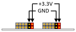
Figure 7.10 – Oscilloscope board power connections
The first step in verifying that there's a proper power connection is to ensure connectivity exists between the GND pins. Connect the black probe on your multimeter to the GND test point on the circuit board. Set the meter to the lowest resistance measurement range, which is typically 200 Ohms. Touch the red probe to each of the four ground pins on the Pmod connectors and verify that the meter drops to a very low resistance reading (less than 1 Ohm).
Next, test each of the +3.3 V pins with the red probe. The resistance to ground is hard to predict, but it should be somewhere in the range of a hundred to a few thousand Ohms. If the resistance is very small – under 50 Ohms – there is probably an unintended short in the circuit. If the resistance is very large – hundreds of kOhms or more – there may be unintended open connections between the power input and circuit components. If any problems are observed, a focused visual inspection of the problem area may identify the issue. If this is not successful, probing with the multimeter at intermediate points in the circuit may help isolate any problems.
With any problems identified during the electrical check resolved, the circuit is ready to be connected to the Arty board. Initial power application will be discussed in Chapter 8, Bringing Up the Board for the First Time.
Summary
This chapter introduced the processes and techniques involved in assembling high-performance digital circuits using surface-mount and through-hole electronic components. A recommended set of tools was identified, including a soldering station, a magnifier or microscope, and tweezers for handling tiny parts. Procedures for solder stenciling and preparing parts for assembly were presented in a step-by-step manner applicable to a wide variety of projects. After soldering, the steps involved in cleaning the board, performing a thorough inspection, and implementing any needed repairs were introduced.
Having completed this chapter, you should understand the tools and procedures required for solder stenciling and the steps involved in preparation for circuit board assembly. You learned how to solder surface-mount and through-hole components to the circuit board by hand and by using a reflow system, as well as how to clean the assembled board and thoroughly inspect it, including checking for electrical short circuits.
In the next chapter, we will power up the completed circuit board for the first time, verify that all the subsystems operate properly, and prepare to implement the remaining system functionality within the FPGA logic and as firmware running on the MicroBlaze processor within the FPGA.