
6
Study of On-line Codes for Baseband Modulation and Carrier Modulation
6.1. Objectives
In this lab work, you will study the various on-line codes for representing the binary information for its transmission on a communication channel. Two sets of codes are studied. The first provides a baseband signal. This one can be sent as it is. It can also modulate a carrier. The various digital modulations with carrier are also available (second way of transmission) and will be studied in principle and technique, especially at the demodulation level.
6.2. Description of the electronic boards
The MODICOM 5 system consists of two electronic boards. The MODICOM 5/1 board includes the conditioning of data (on-line coding) into baseband signals and, if necessary, carrier modulation and thus corresponds to the transmission part. The MODICOM 5/2 board performs the reverse operations and therefore corresponds to the reception part (see the block diagrams on the boards concerned).
The data conditioning part in baseband signals (information-to-signal coding) allows for working with the following on-line codes:
- – NRZ-L coding (level type);
- – NRZ-M coding (Mark (differential) type);
- – RZ coding;
- – Biphase coding (Manchester code);
- – Biphase-M coding (Mark);
- – Bipolar coding (also called AMI coding: Alternation Mark Inversion);
- – RB coding (Return-to-Bias);
- – Quaternary differential coding.
The carrier modulation part performs the following modulation types:
- – ASK modulation: Amplitude Shift Keying modulation;
- – FSK modulation: Frequency Shift Keying modulation;
- – PSK modulation: Phase Shift Keying modulation;
- – QPSK modulation: Quaternary Phase Shift Keying modulation.
The boards MODICOM 5/1 and MODICOM 5/2 are inter-connectable upstream with the MODICOM 3/1 board for the transmitter part (MODICOM 5/1) and downstream with the MODICOM 3/2 board for the receiver part (MODICOM 5/2). The MODICOM 5/1 and 5/2 boards have signal generators with a carrier at 1.44 MHz for one, and a carrier at 960 KHz for the other. Moreover, the latter also has a version in quadrature (Q) relative to the other (I).
More precisely, the MODICOM 5/1 board comprises the following elements:
- – two inputs: a TTL binary signal input (TX DATA INPUT) and associated clock input (TX clock INPUT);
- – direct signal outputs associated with on-line codes and the associated clock;
- – two unipolar-bipolar connection blocks that can be used to build bipolar codes;
- – an inversion block.
In addition, it is possible to simultaneously output a group of two digits (usable for QPSK modulation). Two modulation blocks with carrier and a block of summation make it possible to carry out the various types of digital modulation. On each modulation block, the gain and offsets of the carrier and the modulating signal are adjustable.
Similarly, the MODICOM 5/2 board (Receiver) includes the following elements:
- – a rectifier detector block for amplitude modulation (ASK);
- – a frequency demodulation block (FSK) with phase-lock loop;
- – a phase demodulation block (PSK) with quadratic phase lock loop;
- – a quaternary phase demodulation block (QPSK) with phase-lock loop (with power 4);
- – two low-pass filters;
- – a system for regeneration of bipolar signals into unipolar signals with double thresholds (data squaring circuits);
- – a differential decoder;
- – a clock regeneration system for the biphase code.
6.3. First part – Study of on-line codes for baseband digital transmission
IMPORTANT NOTE.– In all experiments, you will only power the boards (±12 volts; 5 volts) when the wiring has been fully completed and checked.
When using boards MODICOM 3/1 and 3/2, these will be used in the following modes and configurations:
- – selection of fast mode;
- – selection of SYNC CODE DETECTOR mode;
- – no detector and corrector error code mode (A = B = 0);
- – no addition of transmission errors or defects.
6.3.1. Experimental part
From the MODICOM 3/1 board and continuous analog input for it, set the signal amplitude so that the binary word transmitted in serial form by the channel is the following:
for example. However, you can modify the information transmitted at your convenience.
- – Study successively the NRZ-L, NRZ-M, RZ codes and represent their observed chronograms. How does the NRZ-M code compare to the classic NRZ-L code?
- – Study the biphase code (MANCHESTER) and represent the observed chronogram. Explain how the Manchester code works. The next step is to decode the Manchester code. Why does a simple clock regeneration circuit not work?
The clock regeneration specific circuit will be used for the biphase code. What does it produce as a regenerated clock signal?
- – Study the biphase-M code and represent the observed chronogram. Based on your observations, build the biphase-M decoder and explain how it works.
- – Study the bipolar code (AMI code) and represent the observed chronogram. To build it, you will connect the NRZ-M output to the input of the unipolar-bipolar converter and the RZ output to the DISABLE input of the same converter. Study the decoding of the bipolar code and carry it out by using the “Data Squaring Circuits” system and by properly adjusting the two thresholds of the two comparators.
It will then be possible to transmit sinusoidal analog signals over the whole system (MODICOM 3/1; 5/1; 5/2; 3/2) using any of these codes.
6.4. Second part – Study of digital modulations with carrier
We will study successively the digital amplitude modulation and demodulation (ASK), the digital frequency modulation and demodulation (FSK), the digital phase modulation and demodulation (PSK).
In analysis mode, the information sent will be taken equal to “0 1 0 0 0 1 1” for example.
6.4.1. Amplitude shift keying modulation (ASK)
An amplitude modulation will be performed using a modulation block and a 1.44 MHz carrier. The mode of the MODICOM 5/1 board will be set to position 1 and the SYNC CODE GENERATOR of the MODICOM 3/1 board to “OFF”. Perform amplitude demodulation as follows:
The SYNC CODE GENERATOR of the MODICOM 3/2 board will be set to “ON” and the clock regeneration block will be used with an appropriate setting of “PULSE GENERATOR DELAY ADJUST”.
You will adjust the gain and the offsets of the modulating signal and the carrier.
Examine the signals obtained at the output of each of the blocks of the demodulation system (the comparator threshold must be set correctly). Comments.
Change the amplitude of the transmitted signal (MODICOM 3/1) and check that the reconstructed signal is correct by setting the SYNC CODE GENERATOR of the MODICOM 3/1 board to “ON”.
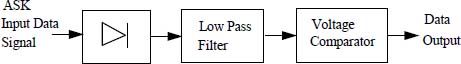
6.4.2. Digital frequency shift modulation (FSK)
Perform a digital frequency modulation according to the block diagram of Figure 6.2.
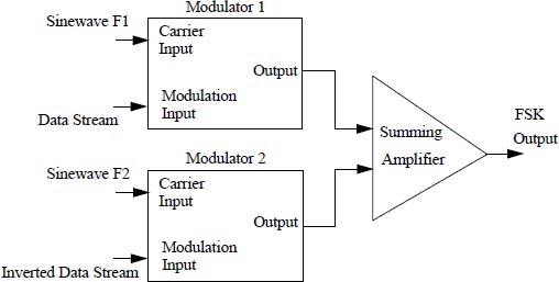
Figure 6.2. Block diagram of FSK modulation
In reception, the signal is decoded by means of a phase-locked loop, a low-pass filter and a comparator, according to the block diagram of Figure 6.3.
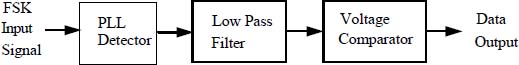
Figure 6.3. Block diagram of digital FSK demodulation
The two boards MODICOM 3/1 and MODICOM 3/2 will be used to generate the information to be transmitted with modulation and to reconstruct the signal on reception. Set the SYNC GENERATOR of the MODICOM 3/1 board to “OFF” and the SYNC CODE DETECTOR of the MODICOM 3/2 board to “ON”.
- – Analyze, for a configuration of information to be transmitted given by “0 1 0 0 0 1 1 1 ”, the modulator and demodulator operations (you will adjust the two carriers used (960 KHz and 1.44 MHz) at the same amplitude. What do you observe before and after the low-pass filter? Adjust the threshold on the comparator so that the baseband signal is correctly reconstructed.
- – By setting the SYNC CODE GENERATOR of the MODICOM 3/1 module to “ON”, the system is fully operational for transmitting analog signals. Analyze the operation of the entire system.
6.4.3. Phase shift keying modulation (PSK)
Perform a digital phase modulation according to the block diagram of Figure 6.4.

Figure 6.4. Block diagram of a digital PSK modulation
In reception, the signal is decoded in two steps.
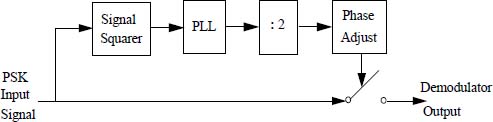
Figure 6.5. Block diagram of a digital PSK demodulation
A demodulator composed of four blocks performs a PSK demodulation (see Figure 6.5).
In a second step a low-pass filter and a comparator provide a logical signal.
- – Show that if the code used at the input of the modulator is an NRZ-L code, there is ambiguity in the decoding.
- – In order to remove this ambiguity, the code used will be an NRZ-M code and the complete scheme to be realized will be the following (Figure 6.6).

Figure 6.6. Block diagrams of a digital PSK modulation and demodulation by using an NRZ-M code
- – A carrier at 960 kHz will be used. Using the word “0 1 0 0 0 1 1” to transmit, analyze the operation of the global system in detail. For that we will use an NRZ-L code at the beginning. Comments.
- – To remove the ambiguity, use an NRZ-M code and analyze the transmission and reception.
Give your general conclusions on PSK modulation.