
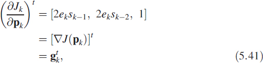
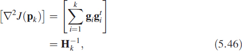
5
Realisation of Digital Filters
Translating difference equations into hardware is an important step in real life, and needs considerable care and attention. There are three distinct elements to this process (Figure 5.1). The first element is conversion of analogue signals to digital numbers; this is accomplished by an analogue-to-digital converter. The second element is implementation of the algorithm; this is carried out in the computing unit. The computing unit may be dedicated hardware made from adders, multipliers and accumulators or it may be a DSP processor. A dedicated unit can be an FPGA unit or a VLSI chip. The third element modifies the output of the computing unit in a manner required for further use in direct digital form or in analogue form. It varies from application to application. Sometimes we may require digitised data for processing.
5.1 Evolution
Hardware realisation of DSP algorithms, or for that matter all the embedded systems, has gone through a revolutionary change in recent years. The reason for this is the phenomenal growth rate of computing power. Clock speeds were around 1 MHz in 1976 whereas today they are 4 GHz or more. Clock speed is a good measure for estimating computing power.
From 1975 to 1985, development was more logic oriented and DSP was always on dedicated hardware. From about 1985 to 1995, it became more software oriented as hardware was becoming standardised while excellent software tools were being created to implement computation-intensive algorithms on single or multiple processors. From 1995 to the present, the line between hardware and software has become very narrow. For that matter, entire design is carried out on electronic design automation (EDA) tools using new methodologies like co-simulation, reducing the design cycle time and providing more time for testing, thus ensuring that the overall system performs closely to the desired specifications.
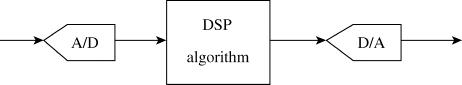
Figure 5.1 General block schematic for a DSP realisation
5.2 Development Process
The development process is depicted in Figure 5.2. There are nine distinct phases in the development process. These phases have remained the same throughout. Understanding the user application constitutes phase 1, based on which a specification document is generated in phase 2. This goes back and forth between the designer and the user, and finally a well-understood document is generated. In phase 3 a detailed design document is produced, which includes as many aspects of the problem as possible, including the development methodology. From 1975 to 1985, on completing phase 3 it was the general practice to go ahead with the coding and run the programs on the hardware by committing them to an EPROM or by testing them on local RAMs.
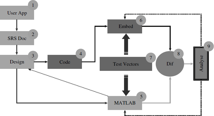
Figure 5.2 How to implement DSP algorithms
The test cycles (moving back and forth between phases 4 and 6) are extremely time-consuming; any errors in the design require an elaborate process of retracing.
Phases 3, 4, 6, 8 and 9 are quite often moved back and forth till the desired goal is achieved. From 1985 to 1995, another path entered the industrial process, one that used to be the domain of the universities. This path has a new phase, phase 5. It is a combination of phases 4 and 6, without hardware but close to reality. Most of the testing is done by moving back and forth in the path 3, 5, 8, 9. It occupies about 30% of the total development time.
Now, with computing power increasing exponentially, electronic design tools for VLSI development can be made available in soft form, so phases 4 and 6 have migrated into phase 5, leading to co-simulation.
5.3 Analogue-to-Digital Converters
In any hardware realisation for DSP, the most important component is the analogue-to-digital (A/D) converter 1. There are many commercial vendors specialising in many different approaches. Some of these approaches are described below.
5.3.1 Successive Approximation Method
Successive approximation is similar to the binary search that is practised in software. This scheme needs several important components: a very accurate digital-to-analogue (D/A) converter, analogue comparator, shift register and control logic. Let the signal be y(t) then the D/A converter output is given as ![]() , where ŷk is the digital input. The error signal is
, where ŷk is the digital input. The error signal is
![]()
The DAC output is compared with the analogue signal. The binary signal e(t) is the output of a high slew rate analogue comparator, and ![]() is the output of a shift register. Simple logic is used to shift and set the bit. If e(t) is positive, the bit is set as 1 else 0 and a shift is made to the right. In Figure 5.3, S/H is a sample and hold and its output is yk, SAR is a successive approximation register.
is the output of a shift register. Simple logic is used to shift and set the bit. If e(t) is positive, the bit is set as 1 else 0 and a shift is made to the right. In Figure 5.3, S/H is a sample and hold and its output is yk, SAR is a successive approximation register.
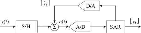
Figure 5.3 Successive approximation method
5.3.2 Flash Converters
In flash converters the given signal x(t) is passed through a sample and hold to obtain xk. This discretised value xk is simultaneously compared with the weights of the full scale range and the result is produced as output of a comparator. Figure 5.4 shows a 3-bit flash A/D converter. The ith comparator output is given as
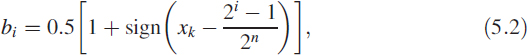
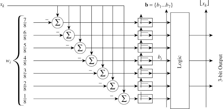
Figure 5.4 Flash analogue-to-digital converter
where n is the desired conversion width. Equation (5.2) is shown in Figure 5.4 implemented in analogue form. The weight wi = (2i − 1)/2n is obtained using a resistor in a potential divider formation. Comparators are high slew rate operational amplifiers specifically designed to meet the speed requirements. A vector b = [b1, b2, …, bn−2, bn−1] is generated and encoded in the desired format using a logic function providing the digital output as ![]() .
.
Notice this scheme has complex hardware. There are many methods available in the literature [4] to obtain higher-order conversions using 3-bit flash converters.
5.3.3 Sigma–Delta Converters
In sigma–delta converters (Figure 5.5) the signal y(t) is compared with a binary signal bk which indicates whether the signal y(t) is in the top half or the bottom half of the conversion range:

The signal z(t) is passed through a hard limiter generating a bitstream bk.
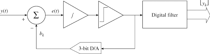
Figure 5.5 Sigma–delta converter
5.3.4 Synchro-to-Digital Converters
It may seem odd to talk about synchro-to-digital (S/D) converters but a close look indicates that they are functionally similar to A/D converters and offer an interesting mathematical viewpoint. The position on a rotating system is uniquely depicted as a 3-tuple Θ = [υ1 υ2 υ3]. This vector is mapped into a scalar as Θ → θ through a table. In simple terms it is a mapping function from ![]() 3 to
3 to ![]() . This is mathematically the same as finding a direction using an antenna system (Section 6.2).
. This is mathematically the same as finding a direction using an antenna system (Section 6.2).
5.4 Second-Order BPF
Suppose the following transfer function is to be realised in hardware. The block schematic will be as shown in Figure 5.6.

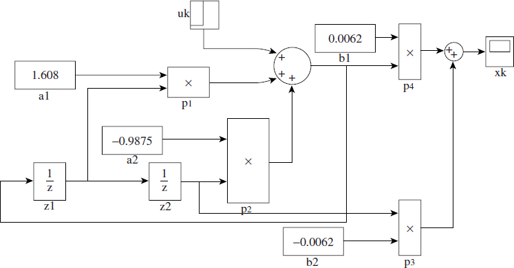
Figure 5.6 SIMULINK implementation of a second-order filter
The above z-domain filter can be readily rewritten as difference equations in the time domain:
![]()
![]()
This requires us to perform four multiplications and three additions. We can see that not all the multiplications and additions are serial. The way we have written the original filter (5.4) as a set of two independent difference equations with minimum delays gives an important clue about the realisation. Equation (5.5) needs two multiplications and two additions, and the multiplications can be carried out simultaneously. Figure 5.6 shows a SIMULINK1 implementation of the filter. There are many third-party vendors providing code generation packages on your chosen processors.
5.4.1 Fixed-Point Implementation
We have directly implemented a filter given as H(z) into floating-point hardware. This may not always be the case. For greater speed and for other reasons such as cost and maintainability, the fixed-point implementation is still a very useful architecture.
This needs a different approach. As a first step, we need to convert the filter coefficients into rational numbers (of the form p/q). The denominator will be a number of the form 2N, where N is an integer:
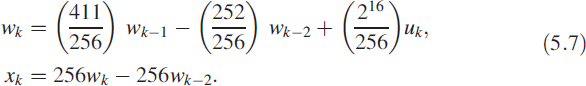
In this numerical example we have N = 8. This means the input is first required to be shifted left 16 places for making a multiplication with 216. It means that we need a 24-bit adder if the input is an 8-bit A/D converter. On making fixed-point multiplication and addition, we shift right 8 times for dividing by 256 to generate wk. The fixed-point implementation is shown in Figure 5.7. Each register provides the delay and the registers are clocked with a minimum period (tc) equal to the time taken for one multiplication (t*) and one addition (t+), so tc ≥ t* + t+. It means that the output of the register settles only after period td = ts + t* + t+ where ts is the register set-up time. We have used two registers r1 (input ![]() and output
and output ![]() and r2 in the above hardware and the information is sequenced as follows (Figure 5.7).
and r2 in the above hardware and the information is sequenced as follows (Figure 5.7).
![]()
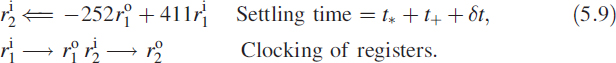
Clocking of the registers can be done only after the combinatorial circuit outputs connected to the inputs of the two registers (![]() and
and ![]() ) settle. Figure 5.8 compares the fixed-point filter with the floating-point filter.
) settle. Figure 5.8 compares the fixed-point filter with the floating-point filter.
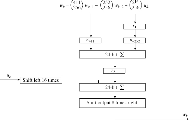
Figure 5.7 Fixed-point IIR filter
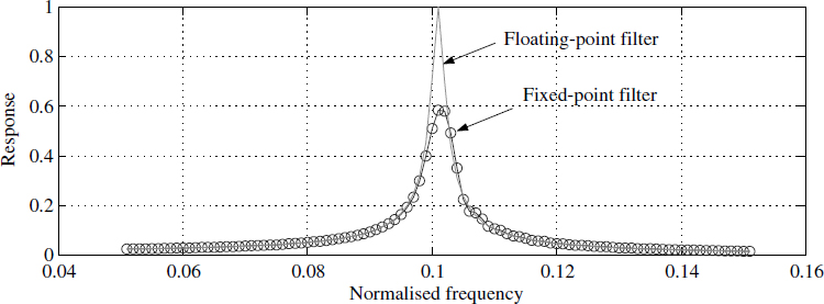
Figure 5.8 Comparison of floating-point and fixed-point filters
5.5 Pipelining Filters
Often the throughput rate is more important than the latency in filter designs. Pipelining is the art of positioning the hardware blocks such that the throughput rate is maximised. Output results are available after every clock cycle.
5.5.1 Modelling Hardware Multipliers and Adders
We introduce ![]() representing a hardware adder and
representing a hardware adder and ![]() representing a multiplier. In reality, all arithmetic operations take a finite amount of time, introducing a delay into the system. Multiplication of two variables, say b1 and uk, in hardware can be modelled as
representing a multiplier. In reality, all arithmetic operations take a finite amount of time, introducing a delay into the system. Multiplication of two variables, say b1 and uk, in hardware can be modelled as
![]()
where * is the ideal multiplier and D1 is the propagation delay associated with the multiplication. The ideal adder is given as + and the corresponding delay associated with the adder is D2. Then an addition of two variables uk and uk−1 can be written as
![]()
Each of the previous devices can be incorporated into a pipelined digital filter structure by following it with a synchronising register. The clock period must then be less than D + ts + tr, where ts is the register set-up time and tr is the register propagation delay. With this notation we can rewrite (5.5) as
![]()
![]()
5.5.2 Pipelining FIR Filters
In this section we wish to realise
![]()
It is acceptable to have an overall delay DN but it is desirable to minimise N:
![]()
First, by associating one D with each multiplier and forming real multipliers as per the notation ![]() , we get
, we get
![]()
Now the real multiplier is formed:
![]()
Next we use one additional D to associate with the adding of ![]() and
and ![]() . It is important to choose the most delayed values first in order to minimise N.
. It is important to choose the most delayed values first in order to minimise N.
![]()
![]()
and using an additional delay D to associate with the final adder, a real adder is obtained:
![]()
Finally, we choose the system delay such that D = z−1 and replace uk−2 = z−2uk and uk−1 = z−1uk, so we get
![]()
Removing the factor z−1 from the expression, we obtain
![]()
Note that N = 2 is the minimum possible value of N for a causal filter. Choosing N = 2 gives
![]()
Equation (5.23) is very convenient for pipelining and is illustrated in Figure 5.9. Hardware enclosed by a dotted line represents a multiplier ![]() or an adder
or an adder ![]() , taking propagation delays into account. The above procedure is general for any FIR filter. Pipelining an FIR filter results in maximising the sampling or throughput frequency at the expense of a delay or latency in the availability of the output. It is like reading yesterday's paper or the day before yesterday's, every morning.
, taking propagation delays into account. The above procedure is general for any FIR filter. Pipelining an FIR filter results in maximising the sampling or throughput frequency at the expense of a delay or latency in the availability of the output. It is like reading yesterday's paper or the day before yesterday's, every morning.
5.5.3 Pipelining IIR Filters
Pipelining an IIR filter is considerably more difficult than pipelining an FIR filter. This is mainly because the delay in the availability of the output makes it impossible to feed back output values with short delay, as is required for the straightforward IIR implementation. As an example, consider a simple first-order IIR filter
![]()
As in the FIR case, we introduce a delay DN as follows:
![]()
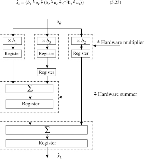
Figure 5.9 Pipelining of an FIR filter
Now we use one delay to form the real multiplier:
![]()
![]()
We use one more D to form the real adder
![]()
Finally, we put D = z−1 and xk−1 = z−1xk to obtain
![]()
![]()
For ![]() = xk, N must be zero. However, N ≥ 1 is required for a causal filter.
= xk, N must be zero. However, N ≥ 1 is required for a causal filter.
Solutions to this problem exist. They use a higher-order difference equation representation of the filter with equivalent characteristics, so feedback loop delay greater than 1 can be tolerated. More details can be found in the literature [2] on pipelining IIR digital filters. In order to pipeline an IIR filter, consider a filter
![]()
The IIR filter defined in (5.31) can be represented using the hardware multipliers as
![]()
Figure 5.10 shows the hardware equivalent of (5.32); adders ![]() and multipliers
and multipliers ![]() are enclosed by dotted lines. This is to indicate that certain IIR filters of this class can be pipelined. Taking this as a hint, we proceed as follows.
are enclosed by dotted lines. This is to indicate that certain IIR filters of this class can be pipelined. Taking this as a hint, we proceed as follows.
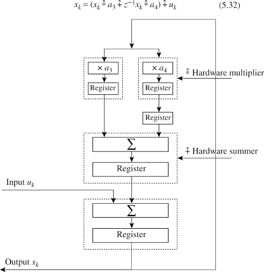
Figure 5.10 Pipelining of an IIR filter
Consider a second-order filter

in which p = 2 cos θ is required to be pipelined. We have demonstrated that all FIR filters can be pipelined and only some IIR filters can be pipelined. With this backdrop, it is proposed to modify the filter in (5.33) as
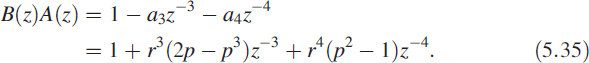
The choice of B(z) is such that the product D(z) = B(z)A(z) is of the form shown in (5.31) and (5.32):
A filter of the form D(z) is highly pipelinable. The choice of B(z) is given as
![]()
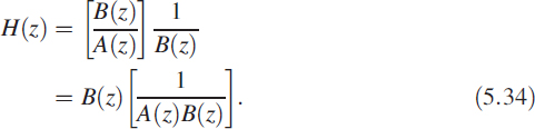
We can see that H(z) is composed of B(z), an FIR filter which is pipelinable, and 1/D(z) and is of the form given by the difference equation (5.31), which is also pipelinable. This implies that H(z) can be pipelined, modifying the structure as H(z) = B(z)/D(z). This method is good but caution must be exercised over the stability aspects.
5.5.4 Stability Issues
We need to look at the stability of the new filter H(z)= B(z)/D(z). The denominator polynomial is D(z) = B(z)A(z), in which the polynomial A(z) is stable. Hence we need to examine the roots of the polynomial B(z) (5.36). Figure 5.11 shows the roots of B(z) at various values of θ for r = 0.9. The unstable regions are marked U. This imposes a limitation on using the entire spectrum, since roughly 50% of the sampling zones are unstable. If we compromise on the the sharpness of the filter, then these zones can be reduced. But by compromising on sharpness, a higher-order FIR filter can probably be used instead of this structure.
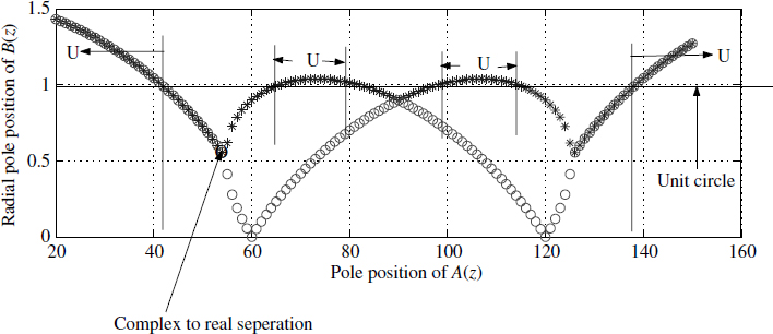
Figure 5.11 Stability of polynomial D(z) in pipelining
5.6 Real-Time Applications
In real-time applications, a single filter or set of filters operate on the data and have to provide the results in a specified time demanded by the overall system requirements. Depending on the time criticality, real-time applications can be implemented using a single processor or using a combination of processor and dedicated hardware. The best examples are the FFT chipsets that were very popular from 1985 to 1993. There are many programable digital filter chips on the market and they can be interfaced to another processor, which may be of low computing power, as a trade-off between cost and hardware complexity. With the availability of powerful processors, almost all the functions can be directly implemented on the same processor.
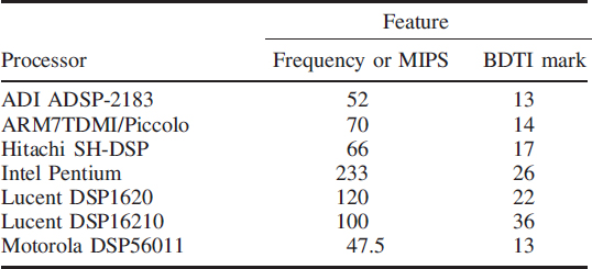
5.6.1 Comparison of DSP Processors
Table 5.1 has been compiled from published literature issued by commercial vendors of DSP processors.2 One important performance measure is the clock frequency or million instructions per second (MIPS). At periodic intervals, Berkeley Design Technolgy Inc. (BDTI) publishes its own processor evaluations based on benchmark programs it has designed.
Table 5.1 Benchmarking some commercial DSP processors
5.7 Frequency Estimator on the DSP5630X
A DSP algorithm implementation on a processor in real time involves three distinct steps:
- Rapid prototyping using MATLAB or any other higher-level language
- Translation to ANSI C and testing the same
- Using a cross compiler to download the code on to the DSP processor
We have implemented this methodology (Figure 5.12) on a DSP5630X processor. Approximately 40% of total development time is invested on algorithm development and 30% is for testing the algorithm.
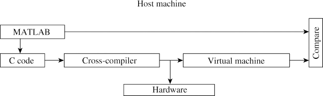
Figure 5.12 Algorithm to hardware
5.7.1 Modified Response Error Method
In the modified response error method [3], the signal yk is modelled as an output of an oscillator corrupted by a narrowband noise ψk and WGN γk. So the modelled signal ŷk can be written as
![]()
The quantity sin(2πfk) in (5.37) can be modelled as an output of an autoregressive second-order system, AR(2), with poles on the unit circle, and is given by
![]()
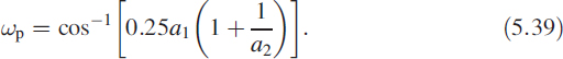
where â1 = 2 cos(ω) and â2 = −1. However, in general a1 = 2r cos(β) and a2 = −r2 where re±jβare the complex conjugate poles. A distinct peak exists [8] at ωp, which is given by
In this problem we shall simultaneously estimate the parameters and the state of the system.
5.7.1.1 Parameter Estimation
In parameter estimation we consider the error ek = yk − ![]() and the objective function
and the objective function ![]() , where the parameter υ is also estimated along with â1 and â2. The choice of ν is such that E[Jk] = 0. For minimising the objective function Jk, gradients are obtained by differentiating (5.38) with respect to â1 and we get
, where the parameter υ is also estimated along with â1 and â2. The choice of ν is such that E[Jk] = 0. For minimising the objective function Jk, gradients are obtained by differentiating (5.38) with respect to â1 and we get
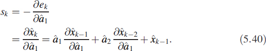
Using (5.40) we obtain the gradient vector as
where parameter pk is given as
![]()
and the value sk is obtained by recasting (5.40):
![]()
We can approximate (5.43) as
![]()
This is due to the fact that (5.43) represents a high-Q filter very close to convergence, hence we can drive the filter using yk to obtain sk due to nonavailability of ![]() .
.
5.7.1.2 Parameter Incrementation
The general incrementation procedure [2] for minimising the function J(pk) is given as
![]()
In the current problem we choose the Hessian [6] as
and the parameter is incremented [7] via
![]()
![]()
A heuristic choice of the step size μk was chosen as the predicted objective function given by
![]()
5.7.1.3 State Adjustment
In state adjustment, the AR(2) process (5.38) which serves as a model has no input added to that at convergence; this AR(2) process is an oscillator. It makes parameter incrementation unstable under normal circumstances. It was found that state adjustment has a stabilising effect and is given by
![]()
5.7.1.4 Frequency Estimation
Frequency is computed by estimating the parameters â1 and â2 and substituting them in (5.39). Note that β is different from ωp.
5.7.1.5 Recursive Estimation
The above algorithm is conveniently represented recursively by using the matrix inversion lemma [1] for obtaining Hk. This algorithm works from arbitrary initial conditions by using a forgetting factor [5] αk while computing Hk. The multiresolution regularised expectation maximisation (MREM) algorithm is as follows:
![]()
![]()
![]()
![]()
![]()
![]()

![]()
![]()
![]()
![]()
![]()
5.7.2 Algorithm to Code
The above algorithm was first implemented in MATLAB and then a C code was written for easy implementation on the Motorola DSP5630X. Both the MATLAB code and the corresponding C code are given in the appendix. Figure 5.13(a) shows the input and the estimated output using the MREM algorithm presented as above. In Figure 5.13(b) we can see the convergence of the parameters. A quick observation shows that a2 is almost one whereas a1 is representative of the frequency.
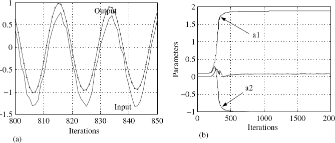
Figure 5.13 Implementation on a DSP5630X
5.8 FPGA Implementation of a Kalman Filter
In this section we implement the algorithm developed in Section 3.11.1. The algorithm is focused on reducing complexity to two FIR filters. Algorithm development is the most critical part of any implementation. In this case the critical aspect is reducing the complex calculations to FIR filters for ease of implementation on field-programable gate arrays (FPGAs). FPGAs are combinatorial circuits which map the design in the form of lookup tables (LUTs). Here are the steps we followed once we had developed the algorithm:
- Algorithm prototype using MATLAB: the rate estimator algorithm was designed using MATLAB and tested.
- Verilog code for FPGA: the derivator was coded in Verilog, simulated on ACTIVE-HDL and synthesised on Leonardo Spectrum. For representing the real numbers we used a sign magnitude fixed-point implementation.
5.8.1 Fixed-Point Implementation
The design of the Kalman filter consists of two FIR filters. FPGAs are better suited to implementing FIR filters than IIR filters. The inputs to the Kalman filter are real numbers; they are represented in fixed-point format rather than floating-point format as floating-point adders and multipliers occupy more chip area on an FPGA. The fixed-point representation is taken to be 6 bits wide since the area occupied on the FPGA will be less. Of these 6 bits, the most significant bit (MSB) is used as a sign bit (zero indicates a positive number and one indicates a negative number), 4 bits are used for the fractional part and 1 bit is used for the integer part (since we are considering normalised data input).
The reason for choosing a sign magnitude representation is the ease of implementation, even though twos complement has a much higher accuracy. The code flow includes implementation of sign magnitude fixed-point adders and fixed-point multipliers.
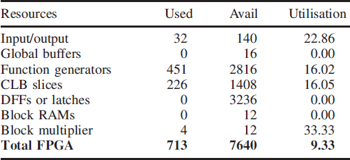
The implementation of the rate estimator was coded in Verilog, simulated on ACTIVE-HDL and synthesised on Leonardo Spectrum. The comparative results obtained from ACTIVE-HDL and MATLAB are shown in Figure 5.14(a) and (b). The target device was the VIRTEX-II PRO. The FPGA results are clipped at the peak (Figure 5.14(b)), but this is only due to the lower resolution (4 bits). The synthesis report in Table 5.2 gives the silicon utilisation. CLBs are configurable logic blocks and DFFs are delay flip-flops.
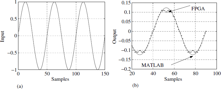
Figure 5.14 Implementation on an FPGA
Table 5.2 Synthesis report for the FPGA implementation
5.9 Summary
In this chapter we described various hardware elements that are frequently used to convert the given analogue signal into digital form. We implemented a second-order BPF in SIMULINK and in fixed-point hardware then compared the results. We looked at a hardware realisation scheme that led us to consider pipelining and its associated problems. We gave an in-depth discussion on various methods of pipelining FIR and IIR filters. Then we looked at a complex algorithm for estimating frequency based on time series data and implemented on the DSP5630X using C. To implement this algorithm using FPGAs, we chose a design using FIR filters.
References
1. K.H. Lundberg, High-speed analogue-to-digital converter survey. Available from www.mit.edu/klund/www/papers/UNP_flash.pdf.
2. M. A. Soderstrand, H. H. Loomis and R. Gnanasekaran, Pipelining techniques for IIR digital filters. In Proceedings of the IEEE International Symposium on Circuits and Systems, New Orleans LA, May 1990, pp. 121–24.
3. K. V. Rangarao and P. A. Janakiraman, A new algorithm for frequency estimation in the presence of phase noise. Digital Signal Processing, 4(3), 198–203, July 1994.
4. M. Yotsyanagi, T. Etoh and K. Hirata, A 10-b 50-MHz pipelined CMOS A/D converter with S/H. IEEE Journal of Solid State Circuits, 28(3), 292–300, March 1993.
5. T. Söderström and P. Stoica, System Identification. Hemel Hempstead, UK: Prentice Hall, 1989.
6. P. Young, Recursive Estimation and Time Series Analysis, p. 25. New York: Springer-Verlag, 1984.
7. D. M. Himmelblau, Applied Non-linear Programming, p. 75. New York: McGraw-Hill, 1972.
8. M. S.E1 Hennawey et al., MEM and ARMA estimators of signal carrier frequency. IEEE Transactions on Acoustics, Speech and Signal Processing, 34, 618, June 1986.