
5
Complex circuits
As you learn to read and draw schematic diagrams, you might get discouraged by the complexities that arise. You might think, “Oh sure, anyone can learn to read schematics of simple circuits, like those that have a transistor or two, a few capacitors, and a few resistors. But it must be impossible to decipher more complicated schematics without decades of experience.” That’s not true! You’ll have to put some effort into the learning process, but you can always break a large, complicated system down into smaller, simpler circuits.
Identifying the building blocks
Even a circuit whose diagram looks overwhelming at first glance comprises multiple building blocks interconnected in an orderly, logical way. This principle never fails! Each building block represents a simple circuit. A device that contains six diodes, 10 inductors, 15 transistors, and dozens of resistors and capacitors might break down into 15 simple circuits, each containing a single transistor, a few resistors and capacitors, and a diode and inductor or two. If you look at the entire system schematic all at once, it’s like trying to eat a jumbo hamburger in a single swallow. With the burger, and with the diagram as well, you face a far easier job if you assimilate the thing in little bites or pieces.
Nowadays, circuits of great complexity are etched onto semiconductor wafers and housed in integrated circuits (ICs), also called chips, that come in packages that actually look like building blocks! As you examine a modern circuit board, you might imagine that the whole system was designed and put together from a block diagram, not a schematic! When you see the complete schematic, it will contain rectangles representing the chips, along with a great many lines connecting them. In most real-world circuits, those lines represent foil runs on a printed circuit board.
Figure 5-1 shows a “crystal radio” receiver built with an antenna, a tapped air-core inductor, a variable capacitor, an RF diode, and a fixed capacitor. The term “crystal” comes from the original construction of RF diodes as they emerged in the early 1900s. In order to get a one-way current gate to act as a signal detector (or demodulator), radio experimenters placed a piece of fine wire called a cat’s whisker into contact with a piece of crystalline lead sulfide called galena. Today, semiconductor diodes do the same thing as those old “crystals” did, even though modern RF diodes don’t look anything like crystals.
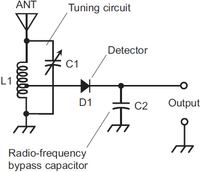
FIG. 5-1. Schematic diagram of a “crystal radio” tuned circuit and detector stages. It produces an extremely weak audio signal.
You can’t call the circuit of Fig. 5-1 “complicated” by any stretch of your imagination, but it performs some sophisticated tricks nevertheless! Aside from the antenna (an external component such as a wire running out your window to a tree) and a sensitive earphone or headphone that you can connect at the output terminals in order to hear radio stations (however faintly), this circuit contains only four components: the coil, the diode, and two capacitors.
You can connect an amplifier to the output of the “crystal radio” in order to boost the audio volume to the point where it can drive a headset to a comfortable listening level. (That’s the reason why Fig. 5-1 doesn’t include a headset at the output.) To accomplish that feat, you’ll need another circuit, along with a battery or other source of DC power to make the output signal strong enough.
Follow the flow
In the “crystal radio,” RF energy from the antenna resonates (reverberates) in L1 and C1. The resonant frequency depends on the size of the coil and also on the setting of C1. That frequency determines which station you hear, if any. Diode D1 converts the signal to pulsating DC that contains both the RF and the audio from the original transmitter. Capacitor C2 shorts the RF part of the signal to ground, leaving only audio-frequency (AF) energy at the output. The position of the coil tap must be adjusted experimentally for maximum output.
Figure 5-2 shows another fairly simple schematic diagram: an audio amplifier that makes use of a single NPN bipolar transistor. In addition, this circuit has four resistors and three capacitors for a total of eight components. It also needs a source of DC power, such as a battery, which provides 12 V. This circuit can accept low-level audio signals (the output of a “crystal radio,” for example) at the input terminals and boost the power to a level strong enough to make a nice loud sound come out of a headset. It might take an experienced engineer two or three minutes to draw the diagram, and a couple of hours to build and test the complete circuit, “tweaking” component values to get the best possible performance.
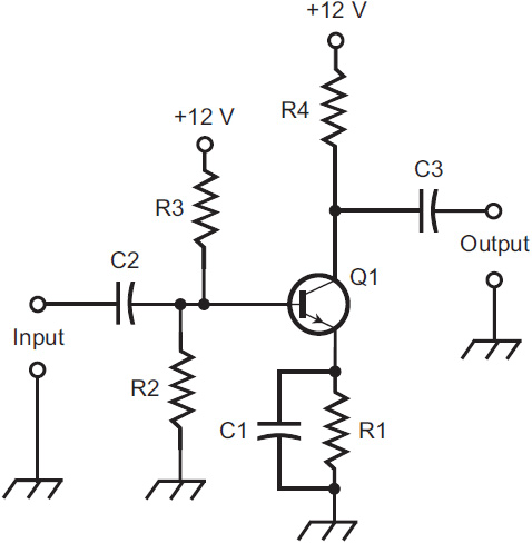
FIG. 5-2. An audio preamplifier circuit that can be used with the “crystal radio” to produce a signal strong enough to drive a headset (but not a loudspeaker).
Because the circuit of Fig. 5-2 takes an extremely weak signal and boosts it to a reasonable (but not particularly powerful) level, it’s sometimes called a preamplifier. If you want to drive a set of speakers so that the students in a classroom, or the audience in an auditorium, can hear the output from the “crystal radio,” you’ll need more amplification. That extra audio boost can be provided by one or more additional circuits called power amplifiers connected to the output of the preamplifier.
In the circuit of Fig. 5-2, audio AC passes from the input through C2 to the base of Q1. The capacitor C2 keeps the power supply’s DC from affecting the behavior of the previous circuit (the “crystal radio” set itself). The tiny current variations at the base of Q1 cause larger current variations through the transistor. The amplified audio signal passes through C3 to the output. The resistors govern the current flowing through Q1, and must be chosen by experiment for optimum amplification. Capacitor C1 keeps the emitter at audio signal ground while allowing some DC voltage to exist there.
Figure 5-3 is a diagram of a circuit that looks, at first glance, more complicated than Fig. 5-1 or Fig. 5-2. But is it really? If you look at Fig. 5-3 for a minute or two, you’ll notice that it’s nothing more than the composite of the “crystal radio” and the audio preamplifier that we’ve just seen. The components are renumbered generally going from left to right, the direction of signal flow through the system. (You never want to duplicate a component designator in any schematic.) In Fig. 5-3, the connection between the original “crystal radio” and the preamplifier corresponds to the short, horizontal connecting line that goes from the dot above C2 to the left-hand side of C3.
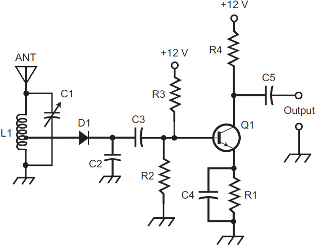
FIG. 5-3. Combination of “crystal radio” and audio preamplifier circuits. Some of the component designators in the preamplifier stage are updated from Fig. 5-2.
Now that you can envision the two building blocks that make up the circuit of Fig. 5-3, the whole diagram looks less complicated, doesn’t it? You can follow the signal flow through the system by thinking of the signal going through the “crystal radio” and then through the audio preamplifier. Of course, the process goes so fast that it would seem instantaneous if you could actually see the RF and audio impulses. The whole process, from the signal arriving at the antenna to the audio appearing at the output, takes place in a minuscule fraction of a second. Currents in electrical conductors, in general, travel at roughly 10 percent of the speed of light in free space. That’s 30,000 kilometers, or 18,600 miles, per second!
The circuit of Fig. 5-3 has a low audio output power level, although it’s a lot louder than the feeble audio signal that comes from the “crystal radio” all by itself, which gets its power only from the signal current in the antenna! Nevertheless, even the amplified audio at the output of the circuit of Fig. 5-3 isn’t enough to provide a comfortable listening volume in a loudspeaker. In order to boost the audio power level some more, you’ll need an audio power amplifier. Figure 5-4 shows a two-transistor circuit that will perform this task. It’s called a push-pull circuit. One of the transistors amplifies the “positive” half of the AC audio wave, and the other transistor amplifies the “negative” half. You might say that Q1 does the “pushing” and Q2 does the “pulling,” so that when you combine their outputs, you get an amplified version of the complete audio input wave.
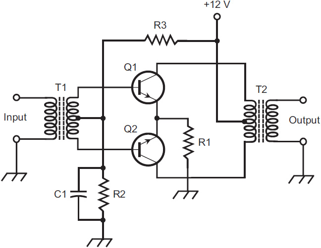
The circuit of Fig. 5-4 will accept the output of a low-level audio amplifier and boost it. However, the output from the original “crystal radio” would not be enough to drive the power amplifier. When you hear the term power amplifier, you should remember that the circuit does exactly what its name implies. It takes an input signal with a certain amount of power and produces an output signal that has more power. If the original input signal contains little or no power, then the circuit of Fig. 5-4 won’t get enough drive (input power) to produce any output signal. In order to work properly, a power amplifier needs a signal that has a modest amount of power to begin with; otherwise it will simply “suck up” the feeble input signal and produce nothing from it other than a tiny amount of heat in the components. The circuit of Fig. 5-3 (the audio preamplifier) provides enough output power to adequately drive a push-pull audio amplifier. The circuit of Fig. 5-1 (the “crystal radio” alone) doesn’t.
In the circuit of Fig. 5-4, the input signal goes through T1 and appears across its secondary. The details of the ensuing process get rather complicated, involving wave phase and transistor characteristics—technical matters that go beyond the scope of this book. Basically, Q1 handles half of the signal cycle and Q2 handles the other half, as the audio input AC flows alternately up and down through the secondary winding of T1. Transformer T2 combines the two amplified cycle halves back into a complete AC audio wave that’s stronger than the wave that came in through T1, thanks to the transistors.
Now if you combine the circuits from Figs. 5-1, 5-2, and 5-4 in cascade (one after the other), you get a complete amplitude-modulation (AM) radio receiver that will produce decent sound from a loudspeaker! Figure 5-5 shows the entire three-transistor AM radio receiver in a single schematic diagram. Again, some of the component designators are changed from previous diagrams, so that they increase generally as you go from the original input at the antenna to the final output at the speaker.
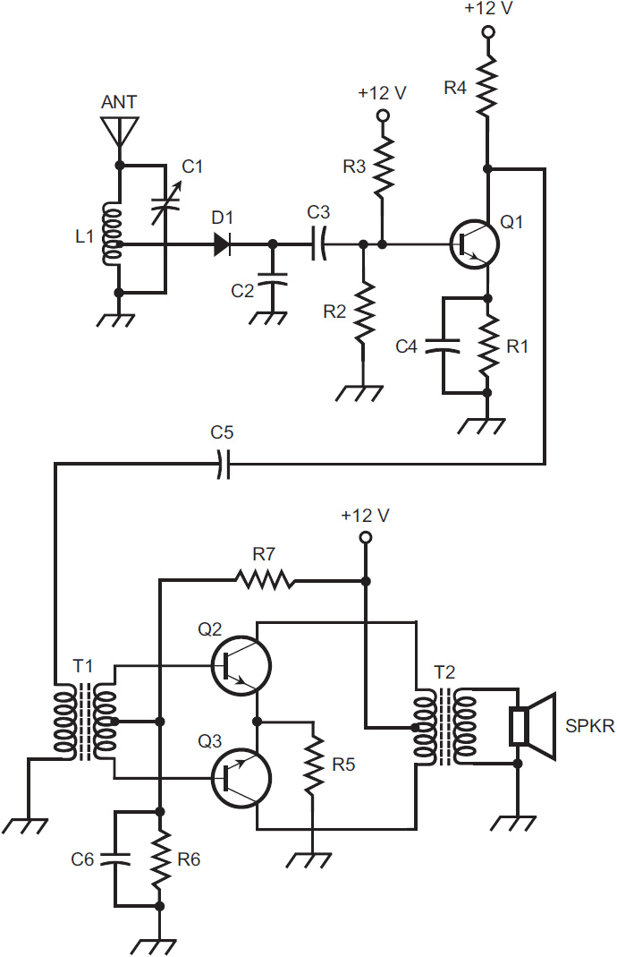
FIG. 5-5. Complete radio receiver circuit. Some of the component designators in the audio power amplifier stage are updated from Fig. 5-4. The speaker is also shown.
So there!
If you were to have seen Fig. 5-5 at the start of this chapter, you might have experienced some major frustration. But now that you can see how the building blocks go together, you know that you don’t have to “choke down the whole burger in one gulp.” So it’s pretty simple after all, isn’t it?
The basic process used to make all electronic circuits breaks down into a sequence of combinations. First, the individual components (resistors, capacitors, diodes, and so on) combine to form simple circuits. Then, simple circuits combine to make more complex circuits. After that, complex circuits combine to form complete devices. Several different devices can combine to create a large system. An amateur radio station is a good example of such a system. It might consist of a transceiver (transmitter/receiver in a single box), an antenna tuner, a computer, an interface unit that goes between the computer and the transceiver, and a speech processor that goes between the microphone and the transceiver. Each of these individual devices contains numerous complex circuits, which in turn, comprise multiple simple circuits, which ultimately break down to the individual resistors, capacitors, diodes, transistors, and other components.
Page breaks
Figure 5-5 is a “respectably complicated” diagram. It requires us to draw the system in a “two-story” format with the detector and preamplifier on top, and the audio power amplifier on the bottom. A long, tortuous line, broken in the middle by C5, represents the connection between the preamplifier output and the power amplifier input. There’s nothing technically wrong with this diagram, but some people might rather see it all on one level. In order to put Fig. 5-5 all on one level, we’d either have to make it horribly small, or else draw it sideways on the page. But there’s another option. We can produce it on a foldout page (the sort of thing that they do in those upscale print magazines when they want to show you something spectacular).
We have yet another alternative, though! We can split the diagram up among multiple pages. That approach isn’t necessary here, but when we get to truly complicated systems, such as amateur radio transceivers, television sets, or complete computers, it’s an option that engineers often use. Figure 5-6 shows how we can take advantage of this technique with the diagram of our radio receiver. Figure 5-6A puts the detector and the audio preamplifier right-side-up on a single page along with an output designator that appears as an X inside a wedge-like arrow that points off the page toward the right. Figure 5-6B shows the audio power amplifier with an input designator comprising an X inside a wedge-like arrow that points off the page toward the left.
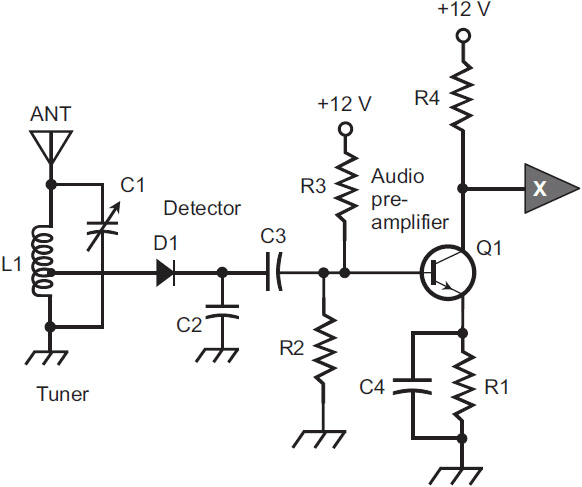
FIG. 5-6A. Tuner, detector, and audio preamplifier stages in the radio receiver. The wedge X represents an extension to illustration B on the next page.
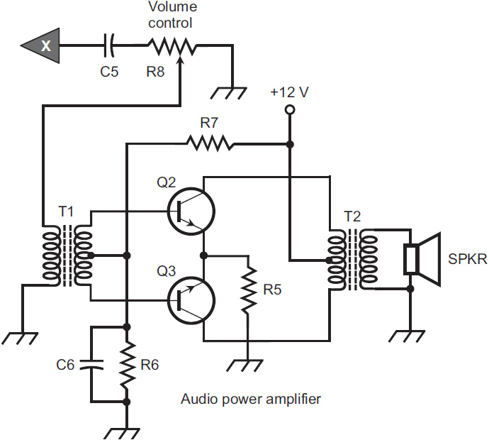
FIG. 5-6B. Audio power amplifier and speaker in the radio receiver. The wedge X represents an extension from illustration A on the previous page.
Tip
In Figs. 5-6A and 5-6B, the wedge-like arrows represent points meant to connect directly to each other. They take the place of the long, tortuous line in Fig. 5-5. In this case, we need only one set of arrows of this type. Some circuits need two or more, so we might label them as X, Y, and Z, for example. Then the two X’s would connect, the two Y’s would connect, and the two Z’s would connect.
Let’s follow the signal through Fig. 5-6A. A radio wave causes current to flow in the antenna, and also through the inductor L1. Capacitor C1 causes the inductor/capacitor combination (called an LC circuit, where L stands for inductance and C stands for capacitance) to resonate at the frequency of the radio signal that we want to hear. Diode D1 detects the RF signal, splitting the AF and the RF portions apart. Capacitor C3 passes the AF part of that signal along to the base of transistor Q1. Capacitor C2 shunts the RF portion of the diode’s output to ground because the circuit doesn’t need the RF energy anymore, and its presence would only cause trouble. Transistor Q1 acts as an amplifier for the extremely weak AF signal at its base. Resistors R1, R2, R3, and R4 ensure that Q1 gets optimum DC voltage (called bias), so that it will produce the greatest possible amount of amplification. Capacitor C4 keeps the emitter at AF signal ground, while allowing some DC voltage to exist there. The AF output signal, along with some DC from the power supply (+12 V), goes off the page through the rightward-pointing arrow marked X.
Now let’s look at Fig. 5-6B and follow the signal after it comes in from the previous diagram. The AF energy, along with some DC, appears at the leftward-pointing arrow marked X. Capacitor C5 blocks the DC so only the AF wave gets to potentiometer R8, which serves as a volume control. The full AF voltage appears across the entire resistance of R8, represented by its left-hand and right-hand terminals. The slider “picks off” various AF voltages that can range from zero (all the way to the right-hand end of the zig-zag, at ground) to the full audio voltage (all the way to the left-hand end of the zigzag, at C5). This AF voltage goes to the primary of transformer T1. From there, the signal flows in precisely the same way as described in “Follow the flow” for Fig. 5-4. The only difference between this situation and that one lies in the numbering of the component designators. We continue going on upward in numbers from the previous part of the system. We also add a speaker to the output of T2, rather than simply labeling it “Output.”
While looking at Figs. 5-6A and 5-6B, have you noticed that we’ve added labels to each stage to describe its function? You should do that whenever you draw diagrams of multistage systems such as this one, as long as you have enough room on the page. In Fig. 5-6A we see the labels “Detector” and “Audio preamplifier;” in Fig. 5-6B we see the label “Audio power amplifier.”
Some more circuits
Figure 5-7 shows an antenna matching circuit known as an L network. Here, the letter L refers to the general layout of the components in the diagram, not the property of inductance. (Actually, to make the coil and capacitor in Fig. 5-7 actually take the shape of an L in the layout, you’ll have to rotate the page 90 degrees clockwise and then hold it up to a mirror! But you get the general idea, right?)
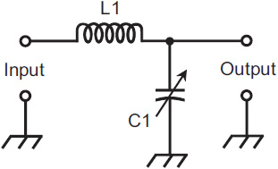
Figure 5-8 shows another type of antenna matching network, which consists of the circuit from Fig. 5-7 with an extra capacitor added at the input end. Engineers sometimes call this type of circuit a pi network because its components, in the schematic layout, resemble the shape of the upper case Greek letter pi (Π). Both the L network and the pi network are commonly used in antenna tuning and matching circuits for radio transmitters at frequencies ranging up to around 150 MHz.
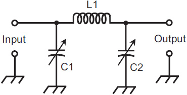
Figure 5-9 shows a circuit that’s a little more complicated than the ones in Figs. 5-7 and 5-8, but in a certain sense, contains both of them put together. When we follow a pi network with an L network, we get a so-called pi-L network. The advantage of a circuit like the one in Fig. 5-9, compared to those in the previous two diagrams, lies in its ability to make radio transmitters work with antennas that would otherwise not accept power very well. Those two extra components can go a long way!
The circuits of Figs. 5-7, 5-8, and 5-9 can all be made more versatile by using variable inductors rather than fixed inductors. One type of variable inductor has become popular among radio amateurs. It’s called a roller inductor. Just for fun, try an Internet search on “roller inductor” by entering the term in the phrase box of your favorite search engine. You should find some images of these components. They allow for precise adjustment of inductance, and some of them have calibrated crankshafts so that you can easily reset them to any previous position.
If you’re old enough, you’ll remember the days when you had to learn the International Morse code (often simply called “the code”) to get an amateur radio operator’s license. Those days have passed into history, but some radio amateurs still enjoy conversing in this mode. In order to do that, of course, you need to learn the code. To that end, you can build a code practice oscillator, such as the one diagrammed in Fig. 5-10. Basically, this circuit is an audio oscillator that you can switch on and off with a Morse code straight key or telegraph key, labeled “Key” in the figure. (Because a telegraph key technically constitutes an SPST switch, you could label it S1.)
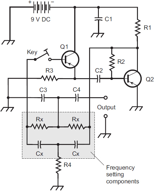
FIG. 5-10. An audio code-practice oscillator using two PNP bipolar transistors. The values of Rx and Cx determine the frequency.
When you first examine Fig. 5-10, you might wonder why an audio oscillator circuit has to be so complicated. Can’t you just build a simple audio amplifier, like the preamplifier or power amplifier discussed earlier, and feed some of the output back to the input? Well, yes, you can in fact do that; but if you want a decent audio tone to come out of your code practice oscillator, you’ll get a lot better results with a circuit like the one in Fig. 5-10. This particular circuit is called a twin-T oscillator because of the T-shaped configurations including the resistors marked Rx and the capacitors marked Cx. The twin-T oscillator produces an AF tone that’s pleasing to the ears, and that also occurs at a predictable and stable pitch (frequency).
The AF signal in the circuit of Fig. 5-10 goes around and around; that’s how oscillation happens. We can start pretty much anywhere and follow the signal back to the same point. If we begin at the key, the signal goes into the base of Q1, where it’s amplified and undergoes phase inversion (the wave is turned upside down). The output of Q1 comes from the emitter of Q1, rather than from the collector; that’s a matter of engineering choice because it provides a stable and reliable circuit. The signal then goes into the base of Q2, where it’s amplified and inverted again, so it comes out of Q2 in phase coincidence (reinforcing rather than opposing) with respect to the signal at the key. The signal emerges from the collector of Q2 and gets routed down to the twin-T network comprising resistors Rx and capacitors Cx, whose values determine the frequency of oscillation. From there, the signal goes back to the key, and gets ready for another round trip through the whole circuit! We take the output through C4, from the point between the two resistors Rx.
The circuit of Fig. 5-10 uses a 9-V battery as its power source. Note that the transistors are of the PNP type, so the collectors get a negative voltage, while the positive battery terminal goes straight to ground. This circuit, therefore, constitutes a positive-ground system. We might build a power supply designed to produce -9 V DC from the AC utility mains (about 120 V AC at 60 Hz in the United States), rather than relying on a battery. If we decide to do that, we’ll need to make sure that we design the power supply so that it produces a negative voltage, not a positive voltage, with respect to ground.
Figure 5-11 shows a power supply that will do a good job of providing a constant, pure –9V DC. It’s just about the same circuit as the one you saw back in Chap. 4 at Fig. 4-13. The basic component layout is the same, except that all the diodes go in the opposite direction in Fig. 5-11 as compared to Fig. 4-13 (including the Zener diode), and the electrolytic capacitor polarity is reversed. And of course, the voltage of the power supply shown in Fig. 5-11 is lower than the voltage of the supply shown in Fig. 4-13.
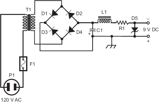
FIG. 5-11. A regulated –9 V DC power supply that can be used with the code-practice oscillator. Note the positive ground in this supply, designed for use with PNP transistor circuits.
Figure 5-12 shows a complete code practice oscillator system that will operate from the AC utility mains. It includes the power supply from Fig. 5-11 along with the oscillator from Fig. 5-10, all in one big schematic. As we did with the radio receiver circuit diagram of Fig. 5-5, we have connected the power supply output to the oscillator in Fig. 5-12 with a single line, although not as long as the one in Fig. 5-5. We’ve also included a volume control and a pair of headphones at the output of the twin-T oscillator circuit.
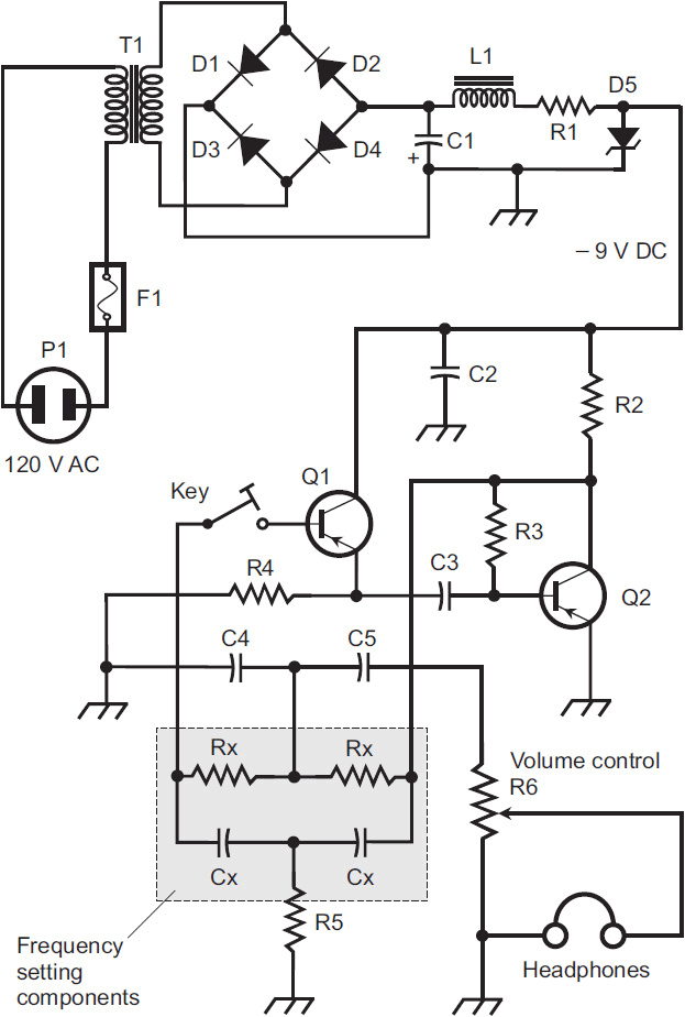
FIG. 5-12. Combination of the regulated power supply and code-practice oscillator. Note the addition of the volume control and headphones.
We can apply the same general layout tactics to Fig. 5-12 as we used with Fig. 5-5. We might draw the diagram with the page tilted sideways (landscape orientation instead of portrait orientation), putting the power supply on the left and the oscillator on the right. Or we might use a foldout page. However, an even better alternative (in my opinion) is to split the diagram up into multiple pages so we can draw everything in an uncluttered, right-side-up fashion.
Let’s take this business a step further. We can boost the output of the twin-T oscillator so that it will drive a loudspeaker, letting us send code to a classroom full of eager Morse-code students! (Finding enough people interested in learning the code to fill up a whole classroom would constitute an entirely different challenge.) A push-pull audio amplifier, just like the one we used for the radio receiver (Fig. 5-4) except with PNP rather than NPN transistors, will work here. Now we have a system with three essential circuits: a power supply, an oscillator, and an amplifier. Figures 5-13A, 5-13B, and 5-13C show how we can draw the complete schematic diagram of this system, letting it spread across three different pages.
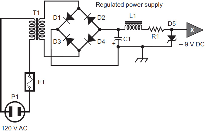
FIG. 5-13A. Regulated power supply for a classroom code-practice system. The wedge X represents an extension to illustrations B and C on the next two pages.
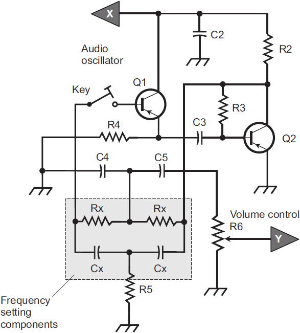
FIG. 5-13B. Twin-T audio oscillator for a classroom code-practice system. The wedge X represents an extension from illustration A on the previous page. The wedge Y represents an extension to illustration C on the next page.
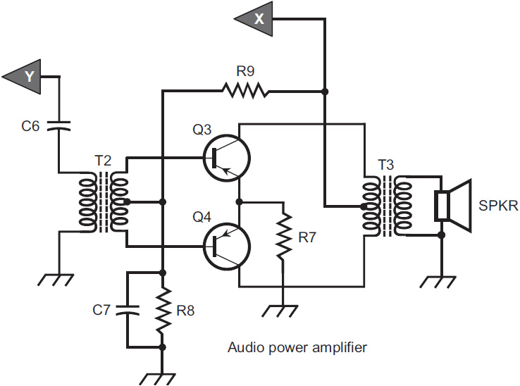
FIG. 5-13C. Audio power amplifier for a classroom code-practice system. Note the PNP transistors, consistent with the negative power-supply voltage (positive-ground system). The wedge X represents an extension from illustration A on the page before last. The wedge Y represents an extension from illustration B on the previous page.
As you examine Figs. 5-13A, B, and C, take careful note of the designators inside the arrows. The right-pointing arrow X in Fig. 5-13A goes to two places on subsequent pages: the left-pointing arrow X in Fig. 5-13B and also the left-pointing arrow X in Fig. 5-13C. The arrows marked Y apply only to Figs. 5-13B and C.
Figure 5-14 shows a simple inductance-capacitance (LC) circuit. Note its resemblance to the L network of Fig. 5-7. In this case, the inductor and capacitor have been reversed from their relative positions in the earlier case. In addition, this circuit has a different purpose than the other one does. The circuit in Fig. 5-7 works mainly for the purpose of tuning an antenna system, or matching the output of a transmitter to the characteristics of a particular antenna. The circuit in Fig. 5-14 is designed to let signals pass through (or not) depending on their frequency. In this case, we have a so-called highpass filter because it lets signals go through more easily as the frequency increases. The exact frequency at which the transition from high attenuation (or lots of signal loss) starts to change over to low attenuation (little or no signal loss) depends on the values of the capacitor and inductor.
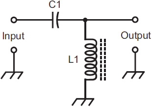
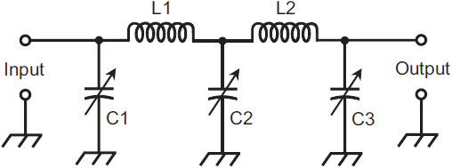
Figure 5-15 shows a more complicated LC circuit that consists of two filters, one after the other. The first filter, made up of capacitor C1 and inductor L1, is the same highpass filter design as the one in Fig. 5-14. The second LC combination, made up of inductor L2 and capacitor C2, forms a lowpass filter. It works in the opposite manner from a highpass filter, letting signals through more easily as the frequency goes down. When we follow a highpass filter with a lowpass filter, and if we choose the cutoff frequencies (or transition points) so that the highpass filter’s cutoff frequency lies below the lowpass filter’s cutoff frequency, we can get a bandpass filter in which a signal can get through easily only when its frequency lies between the two cutoffs.
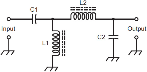
FIG. 5-15. A complex frequency-sensitive filter comprising two simple, but different, filters connected in cascade.
You’ll often find repetition of circuit configurations, one after another, in electronic system design. Sometimes you’ll see several identical or similar circuits connected together. Sometimes their components will all have the same values, and sometimes they won’t. Sometimes the circuits will be connected in series (end to end, like the links in a chain); sometimes they’ll be connected in parallel (across each other, like the rungs in a ladder).
If you know how one circuit in a repetitive system operates, then you know, by extension, how all of the circuits work. A problem that occurs in one circuit might also occur in any of the others, and you can use the schematic diagram to track down the problem. For example, if, through testing, you know that an oscillator has changed frequency because of a defective resistor in the base circuit, then if another oscillator of the same configuration develops the same malfunction, you can consult the schematic, locate the base resistor, and conduct some tests to see if it, too, has gone bad. Without the schematic, you’d have a hard time locating the proper resistor. This single miscreant component that costs a few pennies, could, all by itself, bring down a sophisticated system!
Breaking a massive system down into complex circuits makes it easier to determine which circuit might be creating the problem for the entire system. This complex circuit is then broken down into simple circuits, and a determination is made as to which simple circuit might be at fault. The simple circuit is further divided into separate components, which are examined individually for a possible fault. Through this systematic method of elimination (all done with the help of schematics), the equipment can be repaired with a lot less trouble than you’d experience if you didn’t have the schematics. The process of narrowing-down a problem zone from the system to a complex circuit, then to a simple circuit, and finally to an individual component, is called troubleshooting to the component level.
You’re hired!
If you can troubleshoot large electronic systems to the component level, you’ll find yourself in high demand. All you’ll have to do is show up on time when someone calls you for service, do the job, and leave. When word gets around about your competence and reliability, you’ll have a job for the rest of your life.
Many failures in complex electronic systems arise from a problem with a single component. Sometimes this failure will cause other components to go bad as well, but the repair must start with the first failure. Occasionally, two simultaneously defective components will be discovered, but this sort of coincidence is a rarity. Certainly, you must become familiar with the equipment you intend to repair, but after you have studied and understood the system’s normal state of operation, you can use a schematic drawing to identify the general area of any future faults. By following this procedure, you can identify the most suspect individual component(s). Then all you have to do is find the suspect component(s) in the physical system, get into the equipment with the appropriate test instrument, and check the suspect component(s) one by one.
Tip
Even if you have good test equipment, you’ll find it difficult to quickly identify defective sections (and especially individual components) without a schematic diagram because you probably won’t know where on the circuit board or chassis to look!
Getting comfortable with large schematics
No matter how much you love electronics, you can’t expect to sit down as a rank beginner and read complicated schematics straight away. You’ve got to climb a learning curve. First of all, you must make certain that you know all of the schematic symbols that you expect to deal with. Complex schematics can serve as a great learning tool because they contain lots of symbols, some of which you probably won’t know. Although you can’t sit down with a complex schematic at the start and understand everything that happens in the circuit that it represents, you can use such diagrams to help you learn the symbols.
Once you feel comfortable with the individual symbols, put away the complex schematics and start looking over diagrams of basic, simple, widely used circuits. You’ll find lots of them in magazines geared to electronics enthusiasts. (You’ll find some simple projects and related diagrams in Electricity Experiments You Can Do at Home, published by McGraw-Hill, as well!) Don’t study only one type of schematic, such as those that portray only amplifiers. Check into oscillators, power supplies, solid-state switches, RF circuits, audio circuits, and anything else you can find. You’ll discover similarities between different types of circuits, sometimes with no major differences other than a few changes in the component values. When you can identify an amplifier or oscillator or detector circuit by looking at its schematic, then you’ll know you’re making progress.
Once you can comfortably identify simple electronic circuits from schematic diagrams, you should move on to more complex drawings—but don’t go overboard here! If you try to move too quickly, you might grow frustrated and give up altogether. Your next step will include devices that combine a few of the simple circuits you have previously studied. Sometimes additional components are added to match the output of one circuit to the input of another. Select books and publications that offer both theoretical and practical discussions of the circuit that the schematic depicts. Even better, you can build some simple circuits in a workshop at home.
You’ll likely get a surprise when you see how your first “homebrewed” electronic circuit looks when compared with the schematic drawing. Your study will continue from this point by examining the functional circuit and noting the relationship of the physical components to those in the schematic drawing. You can further your electronics knowledge by experimenting with these circuits (substituting different components, for example). You might find a way to improve the circuit operation. All improvements should be duly noted, and a new schematic can be drawn up indicating your changes. You might want to simply pencil in the changes on the schematic diagram you were building from.
When you feel comfortable building electronic circuits from simple schematic diagrams, you might want to combine two or more circuits to make a single, more sophisticated device. Take two schematic diagrams from a projects book and combine them on paper. You will have to draw your own schematic to serve as your plan for the building procedure. You might know enough by this time to design and build some additional circuits that can interface the two (connect the output of the first circuit to the input of the second one so they both work at their best). When you combine electronics circuit-building with the task of learning to read and create schematics, you can improve your electronics knowledge faster than you can by simply looking at and drawing theoretical diagrams.
Tip
Admittedly, you might start to grow bored as you pore over schematic diagrams for hours on end. But when you can refer to a portion of a schematic drawing and then wire the components in place, much of the boredom will go away. If you’re lucky, or if you happen to be a budding technophile (technology lover), the stuff will get downright fascinating!
Before you know it, you’ll have obtained a solid basic knowledge of schematic diagrams and circuit-building. The circuits that you once imagined as complicated will soon seem familiar and elementary. Nevertheless, you should exercise some caution here. You might feel the temptation to stay with the sorts of circuits that you know best, and not venture into new territory. Don’t let that little bit of laziness get the better of you! As soon as you reach one stage of comfort, move on to diagrams that are more difficult and make you feel a little bit uncomfortable again. If you don’t “push yourself” this way, you’ll find yourself stuck at one stage of development for a long time. Try building more and more complicated devices. Admittedly, this practice can grow expensive if you overdo it; so if you can’t build everything in sight, keep on reading schematics and deciphering the various and diverse circuit components anyway.
You’ll never cease to be amazed at what you know and what you don’t know. For instance, many people new to electronics feel that a commercial AM radio transmitter must constitute a highly complex system. Most electronics novices are astonished to learn that the AM transmitter is technically less complex than an old-fashioned transistorized pocket receiver that you might use to intercept the broadcasts. A commercial radio transmitter is a rather simple system, even though it might have the size and mass of a full-sized refrigerator. The transmitter size is directly related to the component size, which in turn is directly related to the amount of power that the system consumes. The power-supply transformer for a commercial transmitter, all by itself, might weigh as much as the aforementioned refrigerator! This and other components make the commercial broadcast transmitter necessarily large. However, the power-supply transformer for a small amateur radio transmitter will likely weigh less than a kilogram. Schematically, both transformers look the same in schematic diagrams. Circuit complexity bears no relation to the physical size of a component. Complexity depends on the number of components as well as on the number of circuits that the system has.
The massive pieces of equipment are rarely the most complicated ones, both electronically and schematically. The tiny units that can be held in the palm of your hand often take the prize for schematic complexity when you break them down to the component level. A tablet computer is an excellent example. The integrated circuits (ICs or chips) inside a device like that contain millions of individual diodes, transistors, capacitors, and resistors. For this reason, the beginner to electronics and schematics should not shy away from any particular circuit, device, or equipment just because its size suggests complexity. You might be wrong, but even if you’re right, every schematic diagram will contain portions that you can comprehend.
After you have passed the intermediate stage of learning schematics, then you can tackle complex circuits, devices, and systems. You can break them down into multiple-circuit stages or devices, and ultimately into simple circuits. Try to obtain schematics of a complex nature that also include a thorough explanation of how the circuits work.
Recall the block diagram of Fig. 2-2, the strobe light circuit that we saw in Chap. 2. Compare it to Fig. 5-16, a schematic that shows all of the individual components in the circuit. The whole diagram is tilted on its side, allowing it to fit on the page neatly. The circuit is powered with 120 V AC, which comes in at the left side of the schematic (after you’ve rotated the page). The three terminals of the 120 V AC line take three separate paths along color-coded wires. One wire goes to the fuse, another wire goes to the timing components, and the third wire, coming from the ground prong of the plug, goes to electrical ground.
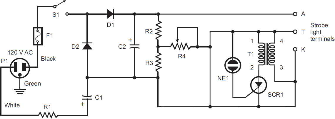
FIG. 5-16. Complete strobe light circuit originally shown in the block diagram of Fig. 2-2 (Chap. 2). In order to fit it on the page, the whole diagram is rotated 90 degrees.
Following the top signal path, current passes through the fuse F1, assuming that the switch S1 is closed. Current then passes through the rectifier diodes D1 and D2 in one direction only. Conventional current travels with the arrows, and electron current goes against the arrows. From the diodes, one path goes all the way across the top wire to the A terminal of the strobe light, and the other path goes to the adjustable timing components comprising resistors R1 through R4, capacitors C1 and C2, and the neon lamp NE1. The adjustable timing components determine the frequency at which the light operates (how long it stays off between extremely brief flashes). The silicon-controlled rectifier SCR1 performs the switching operation for the strobe lamp. Resistors R2 and R3, besides assisting with the timing operation, provide a junction where the bottom portion of the circuit interacts with the top portion, sending the proper signal to the transformer T1 and finally to the strobe lamp terminals T and K.
Figures 5-17A and B show the same circuit as Fig. 5-16 does, except that the diagram is split between two pages so that it can all be presented right-side-up instead of sideways. The first part (Fig. 5-17A) shows the power supply and part of the timing circuitry. The second part (Fig. 5-17B) shows the frequency-adjusting potentiometer R4 along with the rest of the timing circuitry, the switching device, and the transformer that provides the strobe light with the voltage it needs to operate properly.
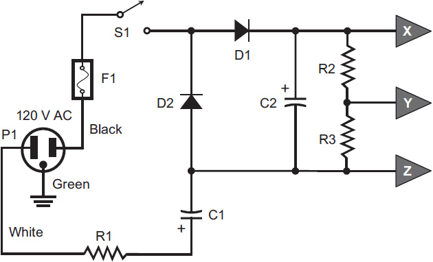
FIG. 5-17A. Plug, fuse, and rectifier portions of the strobe light circuit. Wedges X, Y, and Z represent extensions to illustration B on the next page.
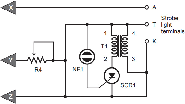
FIG. 5-17B. Timing and transformer portions of the strobe light circuit. Wedges X, Y, and Z represent extensions from illustration A on the previous page.
Summary
Reading and drawing schematic diagrams involves breaking down complex circuits into simple ones. The secret is to look at the system’s parts and how they relate to each other, rather than to regard the whole thing as a huge monolithic entity. As you systematically study a complex schematic drawing, the relationships between the circuits will get more and more apparent. Once in awhile, you’ll suddenly see all of a system’s “secrets” revealed at once: An “Aha” moment!
Tip
When you use schematics for electronics troubleshooting, you won’t always have to understand the function of every single system element. In many cases, you’ll only have to worry about the circuits or components that represent potential trouble spots.
Learning to read and write schematic diagrams is a lot like learning to receive and send the old Morse Code. Morse Code is a language of audible symbols, just like schematic drawing is a language of printed symbols. Once you learn either language, you can use it to communicate; Morse code communicates words and sentences, while schematics communicate principles and concepts.
Using Morse Code as a further example, a long sequence of dots and dashes will mean nothing unless you can break the data down into words. As your proficiency increases, you’ll stop hearing mere dots and dashes (or, as some people say, dits and dahs) and hear letters of the alphabet instead. As you keep practicing with the code, you’ll start to hear entire words. Eventually, if you keep at it long enough (and especially if you get fond of the code for its own sake, communicating with it for hours on end, as I have done over the years as an amateur radio operator), you’ll hear whole phrases and sentences. It will have become a complete language for you.
Reading and writing schematic diagrams follows a similar pattern of development. At first you’ll see individual component symbols. Later, you’ll begin to see simple circuits hidden within complex circuits. Then you’ll be able to identify and decipher complex circuits. Finally, you’ll begin to envision entire systems. This knowledge will not come quickly, but your proficiency will improve every time you practice, if you keep pushing yourself (gently, of course) into new knowledge zones.