
The Power Amplifier
Publisher Summary
The task of a power amplifier is to amplify a processed signal and deliver power into a load such as a loudspeaker. It should do this without introducing spurious signals, such as hum, noise, oscillation, or audible distortion, while driving a wide range of loads. Additionally, it should be tolerant of abuse, such as open or short circuits. Valves designed specifically for audio use generally have optimized configurations that are detailed in the manufacturer’s data sheets. Designing output stages for audio valves from first principles is reinventing the wheel, but an overview of the practicalities is most useful; therefore, one will indulge in a brief analysis of a currently fashionable topology.
The task of a power amplifier is to amplify a processed signal and deliver power into a load such as a loudspeaker. It should do this without introducing spurious signals, such as hum, noise, oscillation or audible distortion, whilst driving a wide range of loads. Additionally, it should be tolerant of abuse, such as open or short circuits. It will be appreciated that this is not a trivial objective, and will therefore require careful design and execution if it is to be achieved.
The determining factor is the output stage. The solution adopted here dictates the topology of the remainder of the amplifier, so we will begin by investigating the output stage.
The Output Stage
Typical audio valves are high-impedance devices and can swing hundreds of volts, but deliver only tens of milliamperes of current. By contrast, a loudspeaker of typically 4–8 Ω nominal impedance requires tens of volts and amperes of current. The obvious solution to this problem is to employ an output transformer to match the loudspeaker load to the output valve or valves.
This is where the problems start. As was hinted earlier, transformers are rather less than perfect, and the ultimate quality of a valve amplifier is limited by the quality of its output transformer. Despite this, the transformer coupled output stage is a good engineering solution, and is used in most valve amplifiers (see later for Output Transformer-Less designs).
Valves designed specifically for audio use generally have optimised configurations that are detailed in the manufacturer’s data sheets. Designing output stages for audio valves from first principles is reinventing the wheel, but an overview of the practicalities is most useful; therefore, we will indulge in a brief analysis of a currently fashionable topology.
The Single-Ended Class A Output Stage
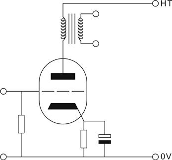
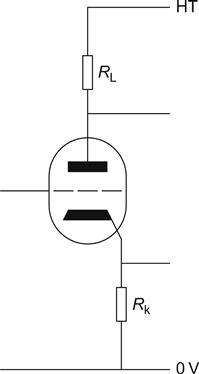
A typical transformer coupled output stage is the familiar common cathode triode amplifier using cathode bias (see Figure 6.1).
When we investigated voltage stages, we used a loadline to choose the value of anode load, and generally optimised for linearity, rather than voltage swing; this time, we need to maximise power. For this example we will use an E182CC double triode, which might be useful as a headphone amplifier. We would normally set the operating point at the intersection between maximum continuous anode voltage (Va=300 V) and maximum anode dissipation (Pa=4.5 W). But as there is a grid curve intersecting at Va=295 V, the operating point has been moved for convenience. For maximum output power, the optimum load for a triode is 2×ra. In our example ra is 3.57 kΩ, so RL=2×ra=7.14 kΩ, and we plot this loadline (see Figure 6.2).
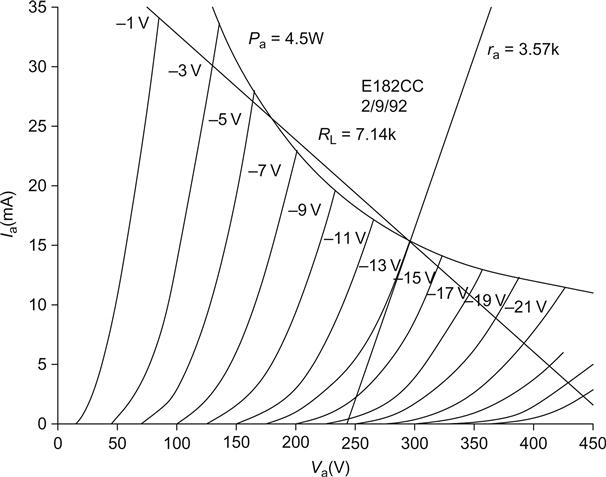
Vgk=−1 V is our positive limit from the bias point of Vgk=−13 V, therefore the negative limit will be Vgk=−25 V for a symmetric input voltage. This results in a peak to peak output voltage swing of 430 V to 85 V=345 V, or 122 VRMS, which equals 2.1 W dissipated in the load. Under these conditions, 4.5 W is dissipated in the valve, giving an efficiency of 32%.
We should now observe some important points about the operation of this stage:
• The loadline strays into the region where Pa≥4.5 W. Since the stage is driven only with AC (it must be, as we could not otherwise transformer couple to the load), this is not a problem. This is because although on one half-cycle the anode dissipation is ≥4.5 W, on the other half-cycle it is less, and the thermal inertia of the anode will average the dissipation out at ≤4.5 W.
• We set the operating point of the valve at 300 V. If the transformer is perfect, then there will be no DC voltage dropped across the primary winding, and so the HT voltage must be 300 V. Yet we have allowed Va to rise to 430 V, which is considerably above HT. This is possible because the transformer stores energy in the magnetic flux of its core. In theory, a perfect valve could swing Va from 0 V to 2×HT, which is a very useful feature in a power amplifier.
• We carefully set our anode load at 7.14 kΩ, but in doing so we assumed that the loudspeaker was a resistor. Loudspeakers are not resistive, and the transformer is not perfect, so the actual load seen by the valve will not be a precise resistance, but a complex and variable impedance.
The valve therefore sees an AC loadline that is an ellipse with its major axis roughly aligned with the theoretical resistive loadline. The gradient of the major axis is the resistive component, and the width of the minor axis indicates the relative size of the reactive component. This means that most of the calculations we can make for an output stage are informed guesses at best, and there is little point worrying about precise values.
• Because we wish to maximise the power in the load, we have to maximise the anode voltage swing, resulting in poor linearity. We could improve linearity by increasing the value of the anode load and plotting another loadline, but this will reduce available output power.
Although the linearity of single-ended stages is not good, the distortion produced is mostly second harmonic, which, as we observed earlier, is relatively benign to the ear. We can estimate the percentage of second harmonic distortion from the following formula:
In our example, Vmax=430 V, Vmin=85 V and Vquiescent=295 V, resulting in 11% second harmonic distortion at full output. Clearly,>10% distortion is not Hi-Fi, but the attraction of single-ended amplifiers is that their distortion is always directly proportional to level, and so at one-tenth output power, the distortion would be ≈1%, and so on. Since, most of the time, music requires very little power, it is often argued (oddly enough, by single-ended enthusiasts) that it is the quality of the first watt that is important, not the remainder that are rarely used. The distortion could be reduced by negative feedback, but this technique is almost universally shunned by the supporters of single-ended amplifiers, so single-ended amplifiers not only produce high distortion, but also tend to have an output resistance of half the assumed load resistance.
The Significance of High Output Resistance
The vast majority of modern loudspeakers use moving coil drivers in sealed or reflex boxes. The theory of the interaction between moving coil loudspeakers and their enclosures was introduced in a landmark series of papers by A.N. Thiele and R. Small in the Journal of the Audio Engineering Society in the early 1970s. A closed box is a second order high-pass filter, whereas a reflex box is fourth order, although it can be designed to look like third order. The crucial point is that Thiele and Small showed that the Q of the high-pass filter could be precisely set by the series contribution of voice coil resistance, crossover resistance, and amplifier output resistance, which is normally assumed to be zero. Typical single-ended amplifiers make a mockery of the zero output resistance assumption and cause the loudspeaker to produce a peaked bass response that the loudspeaker designer did not intend.
Reflex loudspeakers developed prior to Thiele and Small relied on the mechanical damping contributed by the suspension of the loudspeaker to determine bass response and made few assumptions about amplifier output resistance. Horns rely on the transformed air load for damping, so they too are tolerant of high amplifier output resistance. As a further bonus, both of these types of loudspeakers are sensitive, so they are popular with aficionados of single-ended amplifiers.
Bass is produced by moving a large volume of air, and requires a large, rigid, and consequently heavy, cone. Treble is produced by accelerating and decelerating a small area many times a second, requiring low mass. The requirements for bass and treble reproduction are contradictory, so most loudspeaker designers prefer to use optimised drivers for specific frequency bands supplied from an electrical filter known as a crossover. Nevertheless, others feel that the practice of multiple non-coincident drivers and crossovers is so fundamentally flawed that they attempt the design of full-range drivers. In practice, the treble response tends to be peaky and directional after 10 kHz, and the low-frequency resonance limits bass to ≈100 Hz, but this is a sizeable proportion of the audio band. Fortuitously, the motion of a full-range driver’s low-mass cone is easily damped, and when mounted on an open baffle, the mechanical damping of the suspension is frequently sufficient. Thus, a sensitive full-range driver mounted on an open baffle can be an ideal match for a single-ended amplifier.
Transformer Imperfections
When we plotted the single-ended loadline, we treated the output transformer as being perfect, but we should now consider how its imperfections will affect the stage. Unfortunately, we pass a constant magnetising current (Iquiescent) through the primary of the output transformer. In order for the core not to saturate, which would cause odd harmonic distortion, we need a large gapped core. Another method of avoiding core saturation is to reduce the number of primary windings, which not only reduces the magnetising effect (ampere-turns, In) of the quiescent current but also reduces primary inductance.
Usually both methods have to be used, which results in a physically large transformer of low primary inductance at the operating point. Because the transformer is so large, it has correspondingly large stray capacitances, so high frequency performance is also compromised. Typically, the transformers used in this way are large, expensive, and have significantly reduced bandwidth compared to an (ungapped) push–pull transformer.
It might therefore be thought that the single-ended transformer-coupled power stage is a complete non-starter, but, curiously, this is not so. If we look at the hysteresis curve for transformer iron, this offers a clue to this topology’s recent resurgence in popularity (see Figure 6.3).
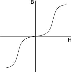
When used as a transformer, the hysteresis curve may be treated as a transfer characteristic showing the relationship between Vin and Vout. If there were no DC current flowing through the transformer, then an AC signal would swing symmetrically about the origin. If we look at the small-signal performance, we see that there is a kink in the characteristic around the origin where the slope of the curve is reduced. Since the core’s permeability is proportional to the slope, the transformer has reduced primary inductance (Lp) at low levels. At low frequencies, reduced Lp reduces gain and increases distortion in the output stage.
The cause of the kink is that the individual magnetic domains that make up the core have stiction in reversing the polarity of their magnetism. (The same effect is true in electrostatics, in that there is stiction in reversing electrostatic charges in polar dielectrics such as polyester and polycarbonate.) A recently popular solution known as pinstriping uses a mix of steel and mu-metal laminations to make up the core. Mu-metal has a much higher initial permeability, so it maintains high Lp at low levels, but saturates quite quickly, at which point the steel takes over, so pinstriping can improve the initial permeability of the core. Unfortunately, mu-metal is fragile and significantly more expensive than steel.
Alternatively, by passing the valve’s quiescent current through the transformer, we ameliorate the problem of low initial permeability making the transfer characteristic more linear, and it is claimed that this is responsible for the excellent midrange detail in this breed of amplifiers. However, a more prosaic explanation is that voice coil inductance causes loudspeaker impedance to rise above 250 Hz, and that when driven from a source resistance of half the loudspeaker’s nominal impedance this typically results in a lift of 3 dB by 3 kHz.
Although the transformer has a low primary inductance, suggesting a poor bass response, a well-designed core is less likely to saturate at low frequencies, since it had to be oversize and gapped to accommodate the quiescent current. Because of this, Lp is nearly constant from full AC output power to zero AC output. Provided that the loudspeaker is carefully matched, a good subjective bass quality can be achieved, because it does not change significantly with level.
Unfortunately, we can make no excuses for the high frequency performance. The large, leaky output transformer has significant losses at high frequency, although excellent construction helps matters.
Single-ended amplifiers typically use true triodes with directly heated cathodes, such as 2A3, 300B, 211 and 845, rather than beam tetrodes or pentodes connected as triodes. Unfortunately, directly heated cathodes are prone to hum when fed with AC, or premature failure when fed with DC, because Vgk at one end of the heater/cathode is lower than the other, causing higher emission at the low Vgk end.
To sum up: single-ended triode amplifiers have good low-level performance but they require careful loudspeaker matching to make the most of their bass performance and low power (usually <10 W), and their cost per audio watt is high due to the expensive output transformer and esoteric valves. But they are simple to make.
Classes of Amplifiers
The ‘class’ of an amplifier refers to the proportion of quiescent anode current to signal current. Until now, we have only looked at Class A amplifiers, although the fact was not explicitly stated. If we relax that restriction, we will need some definitions. Efficiency is defined as:
Although the valve also requires power for the heaters, it is usual to define the ‘power in’ as being from the HT supply.
The following comparisons all assume that the load is coupled to the amplifier by a perfect output transformer because this enables the DC component of the valve’s current to pass through the (reflected) load without loss (no resistive losses in a perfect transformer). Further, the output transformer stores energy in its primary inductance enabling the anode to swing linearly to twice the HT voltage.
Class A
Anode current is set such that even with maximum allowable input signal, current never falls to zero. In other words, the valve never switches off. (Maximum theoretical efficiency of a Class A amplifier is 50% for a sine wave output.)
Class B
There is zero quiescent anode current, and current only flows during the positive half-cycle of the input waveform. The valve is therefore switched off for the negative half-cycle of the input waveform, and considerable distortion of the signal occurs, since it has been half-wave rectified. Additional measures need to be taken to deal with this problem. (Maximum theoretical efficiency for sine wave output is 78.5% for a push–pull Class B amplifier.)
Class C
Anode current flows for less than half a cycle of the input waveform. This method is used only in radio frequency amplifiers where resonant techniques can be used to restore the missing portion of the signal, and results in even greater efficiency and distortion than Class B.
Radio frequency engineers refer to the conduction angle to specify the proportion of time in which anode current flows. Using this description, we see that Class A amplifiers have a conduction angle of 360°, Class B has 180° and Class C <180°. The transition between Class A and pure Class B is quite broad, and so there is an intermediate class known as Class AB (see Figure 6.4).
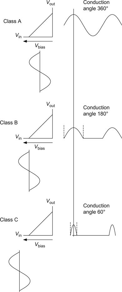
In Figure 6.4, the transfer characteristic of the output device is assumed to be perfect, so the input sine wave is simply reflected through the diagonal transfer characteristic to produce the output. In Class B operation, the bias voltage cuts off the valve, and it is only on positive half-cycles that the signal is able to switch the valve on. It will be noticed that the output waveform of the Class B stage is very similar to the power supply waveforms in Chapter 5 and, for the same reason, half-wave rectification is taking place.
Note that as bias voltage is increased negatively, the conduction angle falls.
In audio, we normally refer to currents rather than conduction angles, and there are subdivisions of classes defined by the grid current of the valve. (RF engineers are unable to do this since they invariably operate with grid current to maximise efficiency at the expense of linearity.)
Class *1
Grid current is not allowed to flow. Many of the larger (≥50 W) classic amplifiers were push–pull Class AB1.
Class *2
The input signal is allowed to drive the grid positive with respect to the cathode, causing grid current to flow. This improves efficiency, since the anode voltage can now more closely approach zero, which is particularly relevant to triodes. At the onset of grid current, the input resistance of the output stage falls drastically (possibly approaching 1/gm), and the driver stage needs a very low output resistance if it is to maintain an undistorted signal into this extremely non-linear load without distortion. Some modern single-ended amplifiers use high-μ transmitter triodes intended for Class B2 operation that pass very little anode current at Vgk=0, so they bias the grid positive to force the required quiescent current, and thus operate entirely in Class A2.
The Push–Pull Output Stage and the Output Transformer
We saw that the Class B stage introduced considerable distortion by half-wave rectifying the input signal. Clearly, this is a disadvantage for a Hi-Fi amplifier, since we require linearity.
Suppose, however, that we had two Class B valves, one fed directly with the input signal, and the other with an inverted signal. During time t1 the upper valve conducts, whilst the lower is cut-off, and during t2, the situation is reversed (see Figure 6.5).
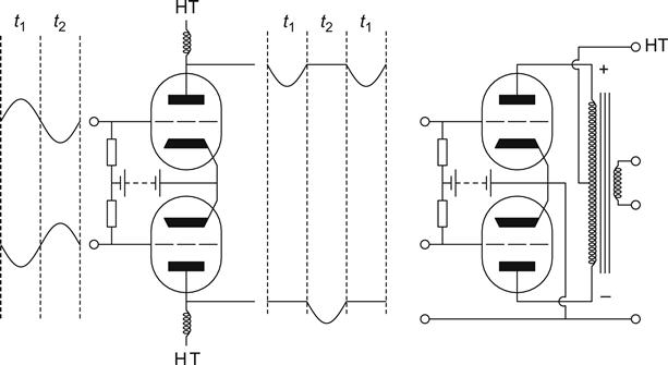
So far all that we have achieved is to ensure that any one valve is switched on, irrespective of incoming signal polarity. However, by inverting one output and summing it with the other in the output transformer, we can recreate the shape of the original input waveform. The inversion is performed by reversing the connection of one winding, and is marked on the diagram with + and – symbols.
Whether achieved by a transformer or by a direct coupled series amplifier, such as a White cathode follower, this form of connection is known as push–pull, and is the only way of approximating linearity in a Class B amplifier.
Unsurprisingly, this dissection of the signal and its subsequent restitching is rather less than perfect, and pure Class B is rarely used because of the distortion generated at the crossover region, where one device takes over from the other. In practice, some quiescent current is allowed to flow in an attempt to smooth the transition, resulting in Class AB operation. The theoretical optimum bias voltage for a Class AB amplifier is found by extending the linear part of the transfer characteristic until it intersects the Vgk-axis. However, practical devices do not operate linearly down to cut-off and then suddenly switch off, so individual differences between devices mean that the ideal point is ill-defined, and crossover distortion is not eliminated.
Push–pull output stages can also be used for Class A amplifiers, giving additional advantages.
Because of the reversal of one winding, the magnetising flux caused by the quiescent anode currents cancels (provided that they are equal). Because the transformer core only has to handle signal current, it does not need a gap and can be far smaller for a given power — this is the main reason for using a push–pull output stage in a Class A amplifier.
Since the core is small, it is important that the quiescent anode current of each valve is identical, otherwise DC magnetisation of the core will generate odd harmonic distortion. This can be done by having an adjustment for DC balance in the bias circuit, or by using pairs of valves with matched anode currents (see Figure 6.6).
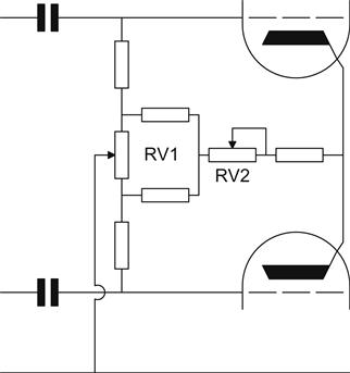
RV2 sets total anode current, whilst RV1 adjusts DC balance by biassing one grid more or less positively than the other.
If the core should become permanently magnetised (perhaps by failure of a valve), it will need to be degaussed, or it will generate additional (and unnecessary) distortion. This can be done by applying a sufficiently large alternating magnetic field to the core to saturate it both positively and negatively, and then reducing the field to zero over a period of about 10 s. In practice, the low remanence of typical transformer core materials means that this procedure is unlikely to be necessary.
A useful consequence of the reduced size of transformer is an improved High Frequency response due to the reduction of stray capacitances.
Not only does quiescent anode current cancel in the transformer, but power supply hum also cancels, since it is in-phase in each winding. Improved tolerance to power supply hum allows a cheaper power supply.
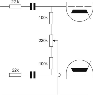
Additionally, even harmonic distortion, caused by unequal gain on positive and negative half-cycles, is cancelled, whilst odd harmonic distortion is summed. Since triodes generate primarily even harmonic distortion, this is useful, but pentodes generate primarily odd harmonics, and therefore require considerable (>20 dB) negative feedback to reduce their distortion to acceptable levels. Cancellation of even harmonic distortion is only achieved if each winding is fed identical signal voltage by its valve, so some amplifiers have adjustments for AC balance, whereas others specify pairs of valves matched for gain (see Figure 6.7).
Modifying the Connection of the Output Transformer
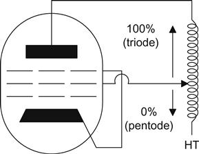
We have mainly considered triodes, and given pentodes scant regard because of their odd harmonic distortion. But if we imagine the output transformer primary as a set of windings that could be tapped at any point, we see that for pentode operation g2 would be connected to the centre tap (0%), whereas for a triode it would be connected at the anode (100%) (see Figure 6.8).
What would happen if we were to tap at an intermediate point? This question was asked in 1951 by David Hafler and Herbert I. Keroes [1], and an amplifier named ultra-linear became synonymous with an output stage that had been invented by Alan Blumlein [2] in 1937. Regarding tapping points, Mullard’s EL84 and EL34 data sheets quite clearly state that 43% gave minimum distortion and 20% maximum power, although it was suggested [3] in 1958 that 20% gave minimum distortion for KT66. This form of distributed loading became almost universal in the final days of valve supremacy, since it combined the efficiency and ease of driving the pentode with much of the improved linearity of the triode. It should be noted that:
And as a consequence, negative feedback at g2 is not as linear a process as one might wish. Nevertheless, almost all power amplifiers using pentodes in the output stage use this scheme because it is far superior to pure pentodes.
Up until now we have placed the transformer in the anode circuit, but we could place the same transformer in the cathode circuit to form a cathode follower resulting in an extremely low output resistance from the valve. As an example, a pair of EL34s, connected as triodes, would each have an anode resistance of about 900 Ω, but used as cathode followers the driving resistance would be a tenth of this at 90 Ω. Reflected through the transformer, the output resistance seen by the loudspeaker would be a fraction of an ohm even before global negative feedback. Unfortunately, there are two crippling disadvantages to this topology.
Firstly, although the output stage is excellent, we have transferred its problems to the driver stage. Each output valve now swings ≈150 VRMS on its cathode, and has a gain <1, requiring ≈500 Vpk–pk to drive it! This can be done, but it is not a trivial exercise to design the driver stage, since we must either use transformer inter-stage coupling, or a resistive anode load requiring a high HT voltage.
Secondly, the high voltage on the cathode of the output valves severely strains the heater/cathode insulation, and can cause premature heater failure. Connecting the heater to the cathode transfers the stress to the heater transformer but requires individual heater windings for each half of the output stage (to avoid shorting k1 to k2), and forces each valve to drive the transformer’s inter-winding capacitance (≈1 nF). In the early days of television, the (expensive) display tube often failed because of leaky heater to cathode insulation, so a service engineer’s fix that avoided the expense of a new tube was to tie the heater to the cathode and supply it from a new transformer rather than including it in the series heater string. But because the 3 MHz bandwidth video signal was applied to the cathode, the transformer needed a low inter-winding capacitance (typically 25 pF), so these were readily available. A similar transformer having multiple low capacitance windings would be ideal for cathode follower output valves.
Alternatively, there are a few valves (usually intended for use as the series-pass element in regulators) whose heater/cathode insulation can withstand 300 V, such as the 6080/6AS7G. Because this valve has such a low ra, its optimum load resistance is fairly low, and its output voltage at full power is also quite low, reducing the strain on heater/cathode insulation. Unfortunately, μ is also very low, so the gain of the output stage is substantially less than unity, and the driver stage has to be quite special (see Figure 6.9).

As can be seen, a complex power supply would be required simply to produce 6 W. Admittedly, the driver could cope with a number of 6080s in parallel, but the cure still seems worse than the complaint. The only reason that this design survived to the drawing stage is that the output stage should be quite tolerant of poor output transformers; conversely, a good output transformer would allow very good performance. The amplifier uses triodes throughout, whose distortion is predominantly second harmonic, but this is cancelled by push–pull action, so the amplifier relies on accurate balance rather than global feedback to reduce distortion, and has a balanced input.
Another form of distributed loading places part of the load in the cathode, and part in the anode; Peter Walker’s Quad II amplifier in the UK used this technique to gain useful benefits from local feedback and distortion cancellation with reasonably relaxed driving requirements. McIntosh [4] in the USA took the technique to its logical conclusion by having equal anode and cathode loads bifilar wound to minimise the output transformer leakage inductance that exacerbated Class B crossover distortion. Sadly, the drive requirements are almost as severe as for the cathode follower, and insulation between the bifilar anode and cathode windings is crucial, so the technique has not been widely adopted (see Figure 6.10).

Each output valve controls its current through equal anode and cathode loads so any change in anode and cathode voltage is equal and opposite. Cross-coupling g2 of each valve to the opposite valve’s anode means that for a given valve, g2 and cathode voltage changes track, implying pure pentode operation, and this is significant because:
• A pentode can swing its anode closer to 0 V, allowing it to deliver more power to the load than a triode.
• A pentode’s g2 prevents feedback from the anode to the control grid reducing gain. We often consider this feedback to be useful (it’s what causes the low ra of a triode), but if we want to apply external feedback, minimising this gain reduction becomes important. Thus, achieving pentode gain before applying transformer feedback maximises the amount of (distortion-reducing) feedback.
The commercial technique of bootstrapping the driver stage’s HT to reduce its distortion and increase voltage swing is a form of positive feedback and makes amplifier high-frequency stability crucially dependent on output transformer design.
Output Transformer-Less (OTL) Amplifiers
Almost all the different output stage configurations were devised in an effort to reduce the adverse effect of the output transformer, so it is not surprising to find that there have been some designs that dispense with the output transformer. These are often known as Futterman [5] amplifiers (who patented the notion), or OTLs.
Driving low-impedance loads directly is not natural for a valve, so radical approaches are needed. High peak currents are required, so valves with robust cathodes are needed, which invariably were not designed for audio, and they therefore have extremely questionable linearity and consistency. Examples are the 6080/6AS7G double triode series regulator valve, and television line scan output valves such as the PL504 and PL519 pentodes. Efficiency is generally on the low side of appalling. Output stages invariably use paralleled White cathode followers with plenty of global feedback to reduce the output resistance (see Figure 6.11).
These amplifiers are quirky in the extreme, yet some designers think that the problems of output transformers are so severe that they persist in making successful OTL amplifiers.
However, the one OTL application where no excuses need be made is headphone amplifiers. Not only do headphones tend to have a higher impedance than loudspeakers (32–300 Ω versus 4–8 Ω) thereby requiring less current, but the close coupling to the ear increases their apparent efficiency and further reduces the current required. The combination of these two factors makes an OTL headphone amplifier not only possible but also desirable, which accounts for the number of recent designs.
The Entire Amplifier
Having looked at the problems of the output stage, we can now consider the support circuitry in detail. We will mainly consider push–pull amplifiers, since they make up the majority of designs, although their design principles may well sbe perfectly applied to single-ended amplifiers. The output stage is insufficiently sensitive to be driven directly from a pre-amplifier, so it needs additional gain. If it is push–pull, it needs a phase splitter. Since linearity is unlikely to be ideal, we will probably need global negative feedback, which will further reduce gain, and this will need to be restored. A complete circuit might therefore comprise an input stage, a phase splitter, a driver stage and the output stage (see Figure 6.12).
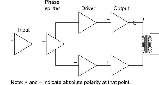
Although a Class A output stage is a constant resistive load, a Class AB2 output stage heavily loads the driver stage when drawing grid current, and its driver stage would need very low output resistance and be able to source significant current to drive this load without distortion.
Unlike the output stage, and possibly the driver stage, the remainder of the stages in a power amplifier will be loaded by predictable resistive loads. It is therefore possible, and desirable, to design these stages with great care in order that they should not degrade the performance of the entire amplifier.
The Driver Stage
Unless the amplifier is quite low power, it will require a dedicated driver stage. We need good linearity, good output voltage swing and, unless we are prepared to add a cathode follower, low output resistance.
The differential triode pair is the ideal choice. The output stage probably requires about 25 VRMS to each grid, and has an input capacitance of 40 pF, or more. An output resistance of 10 kΩ coupled to an input capacitance of 40 pF gives a high frequency cut-off of 400 kHz, which is perfectly acceptable. Since ra≈Rout, the high-μ valves, which tend to have a high ra, are probably unsuitable.
In a properly designed power amplifier, the output stage should be the limiting factor, so we ought to design the driver stage to have at least 6 dB of overload margin. This requirement probably rules out our favourite valve, the E88CC. Very few commonly available valves satisfy our requirements (Table 6.1).
Table 6.1
Dual Triodes Suitable as Drivers
| Type | ra (kΩ) | Comments |
| *SN7/*N7 | ≤10 | Lowest distortion |
| ECC82 | ≤10 | 13 dB worse distortion than *SN7/*N7 |
| E182CC | ≤5 | Good on paper, but can sound strident |
| 6BL7 | ≤3 | Cripplingly high Cag |
| 6BX7 | ≤2 | Capable of driving 845; robust |
The *SN7/*N7 family is by far the most linear of the previous selection, and if the *SN7GTA or *SN7GTB versions are used, Va(max)=450 V. The octal 6BX7 and 6BL7 were designed for use as the field scan amplifier in televisions, but field scan amplifiers are required to be non-linear, so audio performance is variable. In a distortion test of thirty 6BX7 triode sections, the author found that distortion varied by a factor of 4 between samples and that very few envelopes contained a pair of low distortion triodes.
If ultimate performance is required, it is far better to use a pair of single valves and accept that more metalwork is required. The octal 6AH4 is a single triode quite similar to the dual 6BX7, whereas the noval 6S4A is more akin to the 6BL7. Having tested 224 6S4A, the author found that those made by GE were most likely to meet their specification, but Sylvania was the worst (Table 6.2).
Table 6.2
Single Pentodes Suitable as Drivers (When Triode Connected)
| Type | ra (kΩ) | Comments |
| EF184 | ≤5 | Cheap and really plentiful, μ=60 |
| N78 | ≤3 | Uncommon, but dirt cheap |
| A2134, EL84 | ≤2 | NOS EL84 extinct, but current Slovak production fine |
Even lower driving resistance can be provided by an additional direct coupled cathode follower stage, which also has the advantage of buffering the differential pair from grid current effects (see Figure 6.13).
The Phase Splitter
The driver stage is always preceded by the phase splitter, and traditionally the two stages have been combined–although as we shall see, this is not always a good idea. Design of the phase splitter is crucial to the success of a push–pull amplifier, so we will look at this in detail.
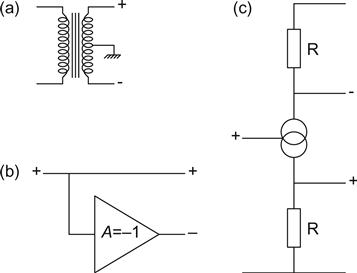
The phase splitter converts a single-ended signal into two signals of equal amplitude, but one has inverted polarity. There are three fundamental ways of achieving this goal (see Figure 6.14):
• We use a centre-tapped transformer in the same way that we use an output transformer to provide inverted and non-inverted signals. All of the previous considerations about transformers apply with a vengeance because of the comparatively high impedances involved, so the technique is not widely used, even though balance is near-perfect under all conditions (see Figure 6.14a).
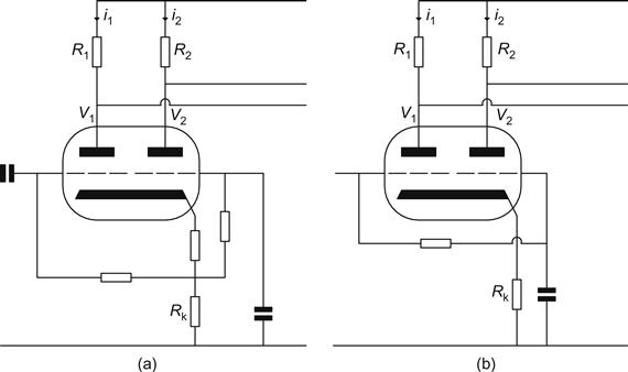
• We have two outputs: one is the original signal, and the other is simply the input passed through an inverter (see Figure 6.14b).
• A valve controls the flow of current between two resistors, one of which is connected to ground and the other to HT. Increased current causes the instantaneous voltage dropped across each resistor to rise, so at any instant the voltage relative to ground is falling at one output, whilst the other is rising (see Figure 6.14c).
The third method is the basis of the concertina phase splitter. Although we will see shortly that the floating paraphase inverter can be a pure expression of the second technique, it is more usual for the second and third techniques to be combined in some form of cathode-coupled amplifier or differential pair.
Triode phase splitters having low resistance outputs are very sensitive to their loading and have different output resistances when both outputs are loaded compared to only one output being loaded. Phase splitters with a high ra have an output resistance dominated by RL, so phase splitters using pentodes and cascodes are immune to loading problems.
Loading sensitivity means that triode phase splitters should only be loaded by a stage that can be guaranteed never to draw grid current because the interaction between phase splitter loading sensitivity and drastically reduced input resistance due to grid current exacerbates distortion caused by grid current.
The Differential Pair and Its Derivatives
Most classic phase splitters were based on the differential pair, and much ingenuity was demonstrated in improving their small-signal performance.
A perfect differential pair comprises two devices having equal load resistances connected so as to allow a signal current to swing backwards and forwards between the two load resistances without any loss whatsoever. Loss of signal current from the cathode to ground impairs performance, so the tail resistance is crucial, and should ideally be infinite.
>RL Solution",5,0,2,1,105pt,105pt,0,0>The Rk>>RL Solution
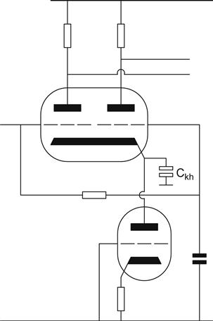
A differential pair can be optimised with a pentode or cascode constant current sink in its tail. An EF184 pentode can achieve a tail resistance >10 MΩ, and even the larger pentodes, such as the EL83, can attain 1 MΩ unaided. Alternatively, we can use a cascoded semiconductor constant current sink, but we will always be limited at high frequencies by Ckh from the differential pair’s cathode, even if the sink is perfect (see Figure 6.15).
The behaviour of the differential pair was discussed in Chapter 2. Provided that Rk≈∞, a balanced output must be achieved if RL1=RL2. Output resistance must also be identical from both outputs, and rout=ra|RL, as before.
However, if only one output is loaded, then:
Loading one output heavily (driving grid current) is equivalent to leaving the other output unloaded, so we find ourselves in the unfortunate situation of driving a condition that requires low source resistance with increased resistance, which is why grid current distortion is exacerbated.
The Rk≈RL Compensated Solution
We accept that we cannot easily achieve a high tail resistance, and do not even try. We use a resistor, typically between 22 kΩ and 82 kΩ, as a tail, calculate what the errors will be, and try to correct them. The principle is often known as the cathode-coupled or Schmitt phase splitter [6] because he was the first to analyse the errors and show how they could be corrected. Practical implementations modify the circuit slightly to accommodate external DC conditions, so the Leak TL series of amplifiers paid the price of biassing their input stage optimally by needing another low-frequency time constant to couple to the self-biased variant (Figure 6.16a), whereas the Mullard 5-20 used the elegant DC coupled Clare [7] variant (Figure 6.16b).
V2 can be considered to be a grounded grid amplifier, fed from the cathode of V1. It is this use of the first valve as a cathode follower to feed the second valve that results in the apparent loss of gain of the second valve, since for a cathode follower, Av<1. By inspection, we see that 2 vgk is required to drive the stage, so the gain of the compound stage to each output is half what we would expect from an individual valve.
If the outputs are in balance, then v1=v2, so:
The gain of V2 is A2, so
The signal current flowing in the cathode resistor is the out-of-balance output signal current:
The signal at the output of V2 must be:
Expanding and collecting I2 terms:
Substituting i1R1=i2R2, and simplifying:
This shows that unless the gain or the tail resistance of the stage is infinite, the ratio of the anode loads should be adjusted to maintain balance. Note that A2 is the individual, unloaded, gain of V2, and not the gain of the entire stage.
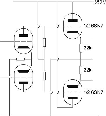
As an example, the Leak TL12+ phase splitter/driver was investigated. This uses an ECC81 and gives a gain of 42 for V2 (R2=100 kΩ, μ=53, ra=26.5 kΩ), R1 should therefore be 91 kΩ, and this is exactly what Leak used (see Figure 6.17).
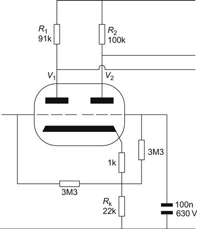
The output resistance of each half of the stage is slightly different because it is in parallel with a slightly different anode load, but curing this in order to preserve High Frequency balance upsets the voltage balance at low frequencies. The nearest approximation that we could achieve is to include the grid-leak resistances as part of the anode loads when calculating the necessary changes. The following grid-leak resistors are 470 kΩ, so RL2=100 kΩ‖470 kΩ=82.46 kΩ, and the gain of V2 falls to 40. The required total load for V1 (including the 470 kΩ grid leak) is thus 75.7 kΩ, and RL2=90.2 kΩ.
Low Frequency balance is determined by the time constant of the grid decoupling capacitor and its series resistor, since it cannot hold the grid of V2 to AC ground at very low frequencies.
Rather than tinker with resistor values whose calculation is critically dependent on valve parameters, the author would rather add a constant current sink to the cathode to force the stage into balance.
The Rk<<RL High Feedback Solution
We make no attempt at providing a large value of tail resistor, and rely on feedback to maintain balance. This circuit was devised by Carpenter [8], but is also known as the floating paraphase or see-saw phase splitter. Typically, the design uses a high-μ valve, such as the ECC83, from whose data sheet this circuit was taken (see Figure 6.18).

If we redraw the circuit (making it identical to Figure 6.6 of Carpenter’s patent), we see that V2 is simply a unity gain inverter, whose gain is defined by resistors R1 and R2 (see Figure 6.19).
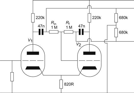
Since the open-loop gain of V2 is not infinite, these values must be adjusted to give a gain of –1. Unfortunately, the calculation is further complicated by the fact that R2 affects the loading, and open-loop gain, of the stage. V2 also requires a build-out resistor to equalise its output resistance, which has been significantly reduced by negative feedback. Once these corrections have been made, the balance of this phase splitter is good, since the operation of V2 is stabilised by negative feedback.
The circuit is analysed by first drawing a DC loadline to correspond to the 220 kΩ anode load. The Mullard operating point is at Va=163 V. The 1 MΩ feedback resistor is in parallel with this at AC, so we draw an AC loadline through the operating point corresponding to 180 kΩ. From this we find that the AC gain of the valve is 67.
We need to find the value of β that will give final gain of 1, using:
We find that β=0.985. The easiest way to achieve this is to increase the value of the feedback resistor:
This gives a value of 1,015 kΩ, so we would add 15 kΩ in series. So far, we have only discovered a 1.5% error, which is trivial, but if we consider the output resistances we find a much larger error. The output resistance of V1 is ra in parallel with RL, and is ≈53 kΩ, but the output resistance of V2 has been reduced by a factor of (1+βA0), from 53 kΩ to ≈790 Ω. 52.2 kΩ of build-out resistance is therefore required, but the nearest standard value of 51 kΩ would be fine. These outputs are then each loaded by 680 kΩ, and if corrections are not made, the output from V2 is ≈6% high.
In practice, these corrections were never made, which perhaps accounts for the poor reported performance of the stage. It might be thought that the cathode coupling would improve balance, but V2 has such heavy feedback that if inadvertently set to non-unity gain (wrong ratio of gain-defining resistors) it can easily overcome any self-balancing action generated at the cathode. The justification for cathode coupling has little to do with improving balance and much more to do with eliminating a pair of undesirable cathode bypass capacitors.
The Concertina Phase Splitter
The phase splitters based on the differential pair were all able to provide overall gain, but once Rk<∞, output balance became partially dependent on the matching of μ between the valves.
Feedback causes the concertina phase splitter to have slightly less than unity gain to each output, and its output balance is almost totally determined by passive components, so valve characteristics hardly enter the picture. Conceptually, operation is very simple. Modulation of grid voltage causes a signal current to flow in the valve, the anode and cathode loads are equal and they have the same current flowing through them, so the signals generated across them are equal, implying perfect balance (see Figure 6.20).
Gain of the Concertina
The gain of the concertina to its anode may be found using the standard triode gain equation, but noting that all undecoupled resistances down to ground via the anode resistance are multiplied by a factor of (μ+1), then:
But for the concertina, Rk=RL, so:
Because of this low value of gain to the anode, Miller capacitance is also low, and the stage has wide bandwidth. Since there is no grid current, anode current is identical to cathode current and applying Ohm’s law to the equal anode and cathode load resistances shows that gain to the cathode is equal to gain to the anode.
Output Resistance with Both Terminals Equally Loaded (Class A1 Loading)
The concertina is a special case (Rk=Ra) of an unbypassed common cathode amplifier with outputs taken from both anode and cathode. The general feedback equation is:
The denominator of the feedback equation is the factor by which resistances are changed and is known as the feedback factor. Since we know the gain of the concertina and the gain of a simple triode amplifier, we can substitute them into the feedback equation to solve for the feedback factor:
Cross-multiplying to find the feedback factor:
The anode output resistance of a common cathode triode amplifier with no feedback is:
The feedback works to reduce anode output resistance, so this value must be divided by the feedback factor (practically, we multiply by the inverse of the feedback factor):
The (RL+ra) terms cancel, leaving:
Initially, it seems most surprising that series feedback (Rk=Ra, after all) should reduce output resistance from the anode so that rout ≈1/gm, but this can be understood by considering an external capacitive load on each output. In the same way that Rk=Ra defines a gain of 1 at low frequencies, so XC(k)=XC(a) defines a gain of 1 at high frequencies, and changing this ratio of capacitances certainly would change the gain, or frequency response at high frequencies, since it would change the feedback ratio β.
Because Zk=Za, the frequency response at each output is forced to be the same, so the output resistances must also be equal, and rout(k)=rout(a).
Concertina Output Resistance, Only One Output Loaded (Class B Loading)
Looking into the cathode, we see Rk down to ground, in parallel with rk the anode path to ground:
Substituting:
Simplifying, and noting that Ra=Rk=RL:
Alternatively,
In a practical application, the (μ+2) term is usually significantly larger than the ra/RL term, so to a reasonable approximation:
Although the cathode output resistance can be calculated fully, the approximation is usually good enough, and generally gives a value of about 1 kΩ.
Looking into the anode, we see Ra to HT, which is AC ground, in parallel with the cathode path to ground:
Substituting
Tidying terms
If we inspect this equation closely, we see that the terms involving μ are the only significant terms, and that if μ is reasonably large, then (μ+1)≈(μ+2), so that rout≈RL. Thus, the concertina suffers a similar weakness to phase splitters based on the differential pair in that one output driving grid current is equivalent to leaving the other unloaded. However, if the cathode output drives grid current, its output resistance remains low, whereas if the anode output drives grid current, its output resistance rises significantly. This imbalance implies that concertina distortion due to driving grid current will contain additional even harmonic components compared to phase splitters based on the differential pair.
It is usual to direct couple to the anode of the input stage, and let that determine the DC conditions of the concertina, resulting in the saving of a coupling capacitor and a low-frequency time constant. Although the concertina is frequently criticised for its unity gain to individual outputs, this is a differential gain of 2, so the combination of input stage and concertina gives double the gain of the same 2 valves used as a phase splitter based on the differential pair.
Phase Splitters and Class B Output Stage Miller Capacitance
If a phase splitter drives a Class B output stage, only one output valve is switched on at any given time, suggesting that there could be no Miller capacitance from the switched-off valve, thereby unbalancing the phase splitter. However, the output transformer acts as an autotransformer, so the valve’s anode still swings and its Cag still has a large voltage across it, causing the charging current that manifests itself as Miller capacitance despite that valve being switched off, so it is not necessary to buffer the phase splitter.
Obviously, the autotransformer argument does not apply to OTLs, but because OTLs have a cathode follower output stage, its input capacitance would be expected to be low. However, because the cathode follower drives such a low impedance load, its gain is very low, so it cannot bootstrap Cgk, resulting in a higher input capacitance than would otherwise be expected. Since OTL output stages are almost inevitably Class AB, on one half-cycle the load is driven by a cathode follower and on the other by an anode follower (common cathode amplifier). The two different amplifiers have entirely different input capacitances (Cga≠Cgk), suggesting that buffering the phase splitter could be worthwhile.
The Input Stage
The input stage is where global negative feedback is applied, so it must provide an inverting and a non-inverting input, both with low noise. The triode differential pair is an obvious candidate for this stage, but the common cathode triode or pentode can also be used, in which case global negative feedback is habitually applied to its cathode (see Figure 6.21).
Design of the input stage is fairly trivial, but can be slightly complicated by the usual practice of direct coupling to the phase splitter, which restricts choice of anode operating conditions.
Stability
When we looked at RC networks in Chapter 1, we saw that a single RC network tended towards a maximum phase shift of 90°. To make an oscillator, we need 180° of phase shift, so a single stage amplifier with one RC network causing an Low Frequency or High Frequency cut-off cannot oscillate. If we cascade two such stages, we can approach 180° of phase shift, and if we feed this back into the input, it will ring, but not oscillate. If we have three such stages, it is a racing certainty that we can make the cascade oscillate when we apply feedback, and this is the basis of the phase shift oscillator.
To achieve oscillation, we need more than phase shift. Just because our feedback signal’s phase has been shifted by 180° will not necessarily generate oscillation. We also need sufficient loop gain. The basis of oscillation is that it is self-sustaining; the gain of the amplifier must be sufficiently high to overcome the losses in the feedback loop before oscillation can occur. Loop gain is thus defined as the gain of the amplifier multiplied by the loss of the feedback loop.
If we have a phase shift of 180° and loop gain ≥1, the circuit will oscillate, and this is known as the Barkhausen criterion.
Now that we have this criterion, we can see how to avoid designing oscillators. We have two weapons at our disposal:
• We can reduce the number of stages, such that phase shift never reaches 180°. We rarely achieve this ideal, because the output transformer plus output stage plus driver stage harbours so many phase shifts, but the principle of minimising the number of stages within a feedback loop is still valid.
• We attack the second condition of the oscillator statement, and reduce loop gain to ≤1 at the troublesome frequencies. This is the basis of all the methods that you will see for stabilising amplifiers, and it is a powerful weapon capable of oppressing anything. Whether the resulting amplifier is of any use may be more debatable.
Slugging the Dominant Pole
This rather vibrant and mystifying description is actually very simple.
A pole in electronic jargon is simply another way of saying ‘high frequency cut off’. What we aim to do is to make the amplifier look as if it only has one High Frequency cut off, which, with a maximum phase shift of 90°, is unconditionally stable. We look for the RC network with the lowest High Frequency cut-off frequency, i.e. the dominant one, and we slug it with yet more capacitance to make it even lower.
Suppose that as a worst case, we cascaded four identical amplifiers, each with an High Frequency cut-off frequency of 300 kHz, and a gain of 10. At 300 kHz, each amplifier contributes a phase shift of 45°, making a total shift of 180°. The gain of each amplifier is 3 dB down at 300 kHz, so the gain of each amplifier at that frequency is ![]() , so the gain of the total amplifier must be:
, so the gain of the total amplifier must be:

In a typical amplifier we might want to reduce this gain from 2,500 to 125, which would be 26 dB of negative feedback, and would reduce distortion to a twentieth of its original value. In order to do this, the feedback loop would have a loss of 0.0076. If we now check for stability, 0.0076×2,500=19. The amplifier has a loop gain ≥1 and a phase shift of 180°, so it will oscillate.
We need to reduce the open-loop gain at 300 kHz by a factor of 19, or 25.5 dB, to achieve stability (this has little effect on the frequency response of the final amplifier). Remembering that 6 dB/octave is equivalent to 20 dB/decade, reducing one cut-off from 300 kHz to 30 kHz will give us 20 dB reduction, and halving from 30 kHz to 15 kHz will give us another 6 dB, making 26 dB in total. This procedure may be formalised by the following statement:
The loop gain may be as large as the ratio of the two most dominant time constants.
To apply this rule, we simply choose how much feedback we want, calculate the loop gain, and adjust the dominant time constant until the ratio between it and the adjacent time constant is equal to the loop gain.
The amplifier is now stable, but only just, and it will ring. We should distance the dominant time constant still further to increase stability and remove ringing, certainly by a factor of 2, and preferably a little more. It should be realised that over-zealous stability compensation reduces feedback, and compromises distortion reduction.
Most practical amplifiers, having exhausted the first two possible methods of achieving stability described, resort to manoeuvring the amplitude response independently of phase response using step networks, usually one inside the feedback loop to manoeuvre the open-loop response and another on the feedback loop to manoeuvre the closed-loop response. Such networks are adjusted on test whilst observing a square wave and typically require simultaneous adjustment of four components (not as hard as you might think).
Realistically, we ought to consider that methods of designing for stability, in priority order, are:
There are some stability problems that are peculiar to valve amplifiers, and they have well-known symptoms and cures.
Low Frequency Instability, or Motorboating
This is an oscillation at about 1 or 2 Hz, and is invariably caused by unintentional feedback via the power supply, due to the rising impedance of filter capacitors at low frequencies. In effect, the entire amplifier becomes a relaxation oscillator [9]. The traditional cure was to insert an low frequency step network, or to reduce the value of the coupling capacitors, in the signal path, so as to reduce the loop gain. This solution molests the second condition of the Barkhausen criterion, but only treats the symptoms.
The real solution is to attack the first condition by removing the filter capacitors and their associated RC time constants by fitting HT regulators. This generally kills the problem stone dead. It is this improvement in stability that is the reason for the superior bass in designs using regulated supplies, since it removes previously unidentified low frequency ringing. It should be noted that this problem does not necessarily need a global feedback loop to make it felt, and ‘zero feedback’ pre-amplifiers are not immune.
It is not unusual to discover that not only is the amplifier motorboating, but that it also has bursts of high frequency oscillation, known as squegging. If possible, it is best to cure the high frequency problem first, since it indicates marginal stability when the amplifier is under maximum stress and may be concealed once the low frequency instability has been cured.
It is possible to build a power amplifier with only two low frequency time constants – one in the output transformer and one in the driver circuitry – but it is so tempting to allow more than one in the driver. We saw earlier that we can have as much loop gain as the ratio of the two nearest time constants, so if we have three time constants that are not widely separated, we must place the middle time constant at the geometric mean of the outer two. Unfortunately, bandwidth considerations force the middle time constant to be the output transformer which, having an iron core, has inductance that varies with level, so its time constant is variable, implying that it is always moving towards one or other of the outer two time constants, reducing stability.
We can now see that the temptation to allow more than one time constant in the driver must be resisted at all costs if Low Frequency stability is to be achieved, so we must now consider whether τdriver should be larger or smaller than τtransformer:
• τdriver<τtransformer: This can be achieved by fitting a small coupling capacitor, but this forces our global negative feedback to correct falling open-loop low-frequency response rather than reducing low-frequency distortion generated in the output transformer.
• τdriver>τtransformer: We know that the output transformer inductance falls as saturation approaches or, to put it another way, it has its largest time constant at low level – which is where it is easiest to test for stability. Thus, there are two advantages to making τdriver>τtransformer:
• Stability increases as output transformer inductance falls.
• Global negative feedback now reduces output transformer distortion rather than correcting falling open-loop response.
Unfortunately, there is a disadvantage. We cannot tolerate blocking at any price because if it occurs it will be prolonged. Thus, the τdriver>τtransformer solution requires that τdriver be implemented before a stage that cannot be overloaded. This is not a problem, but it must be consciously considered.
Parasitic Oscillation and Control Grid-Stoppers
The solution is almost encompassed by the description. Parasitics are the unwanted stray capacitances and inductances that result from the practical attempt to build a component or amplifier.
Miller capacitance in the valve combines with series inductance in the control grid circuit to form a resonant circuit, so valves with a high gm (low rk) are particularly prone to oscillation. (Inductance in the cathode circuit is not a problem because it causes negative feedback that reduces loop gain.) The best cure is to damp the resonant circuit by fitting a grid-stopper resistor in series with the grid as close as possible to the grid pin of the valve base. The physical positioning of the resistor reduces the wire’s inductance (very roughly 0.75 nH/mm), whilst a given value of resistance in the grid circuit is far more effective at increasing the loss of the resonant circuit without compromising frequency response than if it is placed in the cathode circuit. Remembering that:
Thus, Q is most dependent on series resistance, so adding 10 kΩ of series resistance to the grid circuit is a sure-fire way of oppressing parasitic oscillation.
For small-signal valves that are prone to this problem (E88CC, 5842, EC8010) a thin film surface mount resistor actually touching the pin is ideal, whereas leaded carbon film resistors are more convenient for power valves. Typical values range from 100 Ω to 10 kΩ, and are usually found by experiment since individual layout is critical. If you can guarantee >100 MHz bandwidth at your probe tip, use an oscilloscope to determine the smallest acceptable value because excessive resistance increases grid current distortion, but beware that touching the typical 8 pF capacitance of a probe to a marginally stable circuit can sometimes tip the balance between stability and oscillation, so probe at the anode. If you can’t probe, play safe and use a large grid-stopper because unseen RF oscillation always increases distortion.
Parasitic Oscillation of Ultra-Linear Output Stages, and g2 Stoppers
Ultra-linear amplifiers with poor output transformers or parallel pairs of output valves sometimes need a series RC network between anode and g2. This is because this section of the winding has resistance in series with leakage inductance – the additional network attempts to return this impedance to a pure resistance. For 43% taps, the impedance between the anode and g2 tap is≈9% of the total anode to anode impedance, so this is a good starting point for the value of resistor, but both have to be determined empirically (adding them to both halves of the transformer simultaneously, which makes life difficult), and are often around 1 nF and 1 kΩ. Bear in mind that each capacitor has to withstand VHT when the associated anode swings towards 0 V.
Parasitic Oscillation and Anode Stoppers
Now that NOS audio valves are in short supply, it is common to substitute cheaply available RF valves, but (being designed for RF) these can sometimes oscillate at high frequency or VHF. A common amateur radio solution was to add a series anode stopper inductor made from a 2 W 100 Ω carbon resistor overwound with about 10 turns of ≈0.7 mm enamelled copper wire soldered to each end of the resistor – the inductor prevents the valve seeing the capacitance that made it oscillate and the carbon resistor damps the inductor’s VHigh Frequency self-resonance. Exactly the same trick is used at the output of transistor power amplifiers to protect the amplifier from excessive loudspeaker cable capacitance that could cause High Frequency instability and consequent destruction, and it was the absence of this component that caused the wholesale destruction of some well-known amplifiers when low inductance high capacitance loudspeaker cable became briefly fashionable.
High Frequency Stability and the 0 V Chassis Bond
Although we tend to think that we require a low resistance bond at the input socket between the amplifier’s 0 V and the chassis to minimise hum, it also needs to be low inductance to maintain High Frequency stability. There is inevitably stray capacitance between each and every part of the circuit and the chassis. Thus, there will somewhere be two capacitors in series that connect an amplifier’s output back to the input in phase, potentially causing oscillation. Connecting the chassis to 0 V short circuits the junction of those two capacitors to 0 V and breaks that positive feedback loop.
Stability Margin
Stability of valve amplifiers is often described by the amount of additional global negative feedback that would be required to cause oscillation. This is simply the ratio by which the dominant time constants were further distanced, over and above the necessary minimum required for stability. The designers of the Mullard 5-20 were proud to claim that 10 dB more feedback would be required to cause instability, whereas the Williamson is questionable at Low Frequency even without additional feedback.
Unlike a transistor amplifier, it is unusual to be able to apply more than 30 dB of global negative feedback to a valve amplifier, and even then design needs to be planned very carefully to ensure that the feedback reduces distortion rather than stability.
Classic Power Amplifiers
Now that we can recognise and analyse individual stages, we can investigate the design of some classic amplifiers such as the Williamson, the Mullard 5-20 and the Quad II.
The Williamson
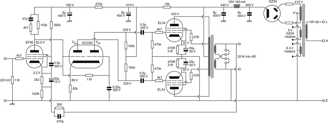
The design of this amplifier was published in Wireless World [10] in 1947, and set a standard of performance that was years ahead of its time.
The input stage is the standard common cathode triode with 20 dB of global negative feedback applied from the loudspeaker output to the cathode. The phase splitter is a concertina circuit direct coupled from the input stage, and feeds a differential pair using both halves of a 6SN7 (see Figure 6.22).
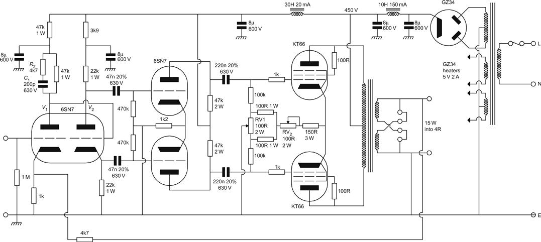
The output stage is a push–pull pair of KT66 beam tetrodes operated as triodes that provide 15 W output in Class AB1, operating mostly in Class A. RV1 adjusts the DC balance of the output valves in order to minimise distortion due to the transformer core, whilst RV2 sets the quiescent current to 125 mA for the entire stage.
The linearity and headroom of each stage is excellent due to the careful positioning of operating points and choice of valves, but because this amplifier has four stages enclosed by the feedback loop, stability needs to be taken very seriously.
The input stage initially has an output resistance of ≈7.5 kΩ, but this is raised by the feedback to ≈47 kΩ. In combination with 12 pF of input capacitance from the concertina, this gives a high frequency cut-off of ≈280 kHz. However, this has been modified by adding the step compensation components R2 (4.7 kΩ) and C1 (200 pF) to the anode circuit of V1. This circuit puts a step in the amplitude response which begins to fall at ≈130 kHz, but the phase response remains virtually unchanged until 280 kHz.
The concertina drives a driver stage with an input capacitance of 60 pF, and because the output transformer for the Williamson was very carefully specified, it seems unlikely that losses in the output transformer would cause the global feedback loop to force the driver stage out of Class A operation. The concertina, thus, faces a balanced load, and has an output resistance ≈350 Ω, resulting in f−3 dB=7.5 MHz, which is sufficiently high to be insignificant.
The driver stage has an output resistance of ≈8.7 kΩ, together with 55 pF of input capacitance from the output stage, the cut-off is ≈330 kHz, and the output transformer is specified to have a cut-off of 60 kHz.
The number of high frequency cut-offs within the feedback loop has not been minimised, and the dominant high frequency cut-off (the output transformer) is rather close to the pair which are next most dominant. Thus, the only remaining way to achieve stability at high frequency was to adjust the phase response independent of amplitude response by means of a step network.
At low frequencies it is more useful to consider time constants than –3 dB points. The input stage is direct coupled to the concertina, so we can ignore this. The concertina feeds the driver stage with a CR of ≈22 ms, as does the driver to output stage, and the output transformer is set to 48 ms. Additionally, the author’s experience has been that decoupling the HT between input stage and concertina can sometimes induce motorboating. In view of this, it is not surprising that Low Frequency stability is questionable, as was conceded in the original Wireless World article. In 1952, Hafler and Keroes decided that their output stage would benefit from a Williamson driver [11], so they quintupled the concertina to driver stage coupling capacitors from 50 nF to 0.25 μF to separate the low-frequency time constants.
It should be remembered that in 1947, circuits were designed using long multiplication or tables of logarithms, and if speed was needed – slide rules. Computer-aided AC analysis was not an option! Most amplifiers were designed as carefully as possible, then adjusted on test for best response – and wide-bandwidth (>1 MHz) oscilloscopes were recently developed luxuries.
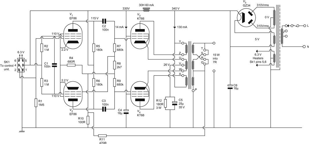
The Mullard 5-20
This was a 20-W design introduced by Mullard [12] to sell the EL34 pentode. There is considerable similarity between this design, the Mullard 5-10 (10 W using EL84), and some Leak amplifiers (see Figure 6.23).
The input stage is an EF86 pentode, which is responsible for the high sensitivity but poor noise performance of these amplifiers. Most of the cathode bias resistance is bypassed, since it would otherwise reduce the gain from around 120 to 33, which would be a waste of open-loop gain that could be used to correct distortion produced by the output stage. Unadorned, the pentode has an output resistance of 100 kΩ, and drives ≈50 pF of input capacitance from the phase splitter, which would give a cut-off of 32 kHz, but this is modified by the usual step network across its anode load.
A slightly unusual feature is that the g2 decoupling capacitor is connected between g2 and cathode, rather than g2 and ground. In most circuits, the cathode is at (AC) ground, and so there is no reason why the g2 decoupling capacitor should not go to ground. In this circuit, there is appreciable negative feedback to the cathode, and so the g2 capacitor must be connected to the cathode in order to hold g2–k (AC) volts at zero, otherwise there would be positive feedback to g2.
The cathode-coupled phase splitter is combined with the driver circuit using an ECC83. When loaded by the output stage, for V2, Av=54, but gain to one output is half this at 27.
The anode load resistors have not been modified to give perfect balance. With the 470 kΩ grid-leak resistors of the output stage in parallel with the 180 kΩ anode loads, the effective anode load is 130 kΩ. Using the formula derived earlier, this means that V2b should have an AC anode load 3% higher than V2a, and RL for V2b would then be 187 kΩ. Mullard did actually state this [12], but probably assumed that most constructors would not have access to sufficiently close precision resistors to use the information.
The output stage has an input capacitance of ≈30 pF, and the driver stage has an output resistance of 53 kΩ when loaded symmetrically, giving a cut-off at ≈100 kHz, which is quite poor. Loaded asymmetrically, the output resistance rises to ≈90 kΩ, which lowers the cut-off to ≈60 kHz.
Looking at the driver stage, we should investigate how capable it is of driving the output stage. 85 V will be wasted across the 82 kΩ tail resistor, but with 410 V of HT, this still leaves us with 325 V. With the component values given, this puts the operating point at 240 V on the 180 kΩ DC loadline. Drawing the AC 130 kΩ loadline through this point shows that the stage would generate ≈4% second harmonic distortion at full drive (Vout=18 VRMS), if it were not operated as a differential pair. Mullard claimed 0.4% distortion for the entire driver circuitry.
Although distortion appears acceptable, the driver stage has only 10 dB of overload capability. When output stage gain begins to fall due to cathode feedback or insufficient primary inductance in the output transformer, or input capacitance loads the driver, the global feedback loop will try to correct this by supplying greater drive to the output stage, and the 10 dB margin will be eroded, increasing distortion.
The driver circuitry was designed to produce an amplifier of high sensitivity even after 30 dB of feedback had been applied, and this has forced other factors to be compromised. Whereas the Williamson sacrificed stability for linearity, the Mullard 5-20 achieves stability at the expense of noise and linearity.
The output stage is a pair of EL34s in Blumlein distributed load configuration, with 43% taps for minimum distortion. Unlike the Williamson, there is no provision for adjusting or balancing bias, and this might seem to be a retrograde step.
Bias adjustment implies connecting the cathodes together and using a proportion of grid bias to provide the balance adjustment. Because the biassing is firmly set by the potentiometers, there is no self-regulation of bias current, and as the valves age, balance will need to be reset. In short, providing this adjustment ensures that it has to be used regularly.
By contrast, the Mullard 5-20 has separate cathode bias resistors and relies on automatic bias to hold the anode currents at their correct, and therefore equal, currents. In practice, this works well, although it does not quite achieve the low transformer core distortion of a freshly balanced adjustable system.
This system does have a disadvantage in that the individual cathode bias resistors apply series negative feedback to the output valves, raising their output resistance. The output transformer could be redesigned to maintain the match to the load, but this is undesirable as it would require a higher primary impedance, which makes a high quality design more difficult to achieve. Because of this, the cathode bias resistors must be bypassed by capacitors, and this is where the problems really begin.
The capacitor is a short circuit to AC, and so prevents feedback, but its reactance rises at very low frequencies, so it is no longer a short circuit, and allows feedback. Because the output stage is matched to the load, the unwanted feedback causes a sharp rise in distortion and reduction of output power due to the mismatch. The obvious solution is to fit a large enough capacitor to ensure that the Low Frequency cut-off for this combination is below all frequencies of interest, perhaps 1 Hz. Remembering that the resistance that the capacitor sees is Rk in parallel with rk, we can easily calculate the value required.
For a pentode, rk=1/gm; a typical output pentode has gm=10 mA/V at its working point, so rk≈100 Ω, which is in parallel with a bias resistor of ≈300 Ω, giving a total resistance of 75 Ω. For 1 Hz, we therefore need 2,000 μF of capacitance.
2,000 μF 50 V capacitors were simply not available at the time, and they weren’t fitted. They are readily available now, but there’s a more subtle reason for using a smaller value. When the output stage is driven into Class B, each cathode tries to move more positively than negatively. It can’t turn off any further, but it can certainly turn on harder. The cathode capacitor integrates these changes into a gently rising DC bias voltage, which biasses the valve further into Class B, and the problem continues. The effect of this is that a momentary overload can cause distortion of following signals that would normally have been within the capabilities of the amplifier – this is a form of blocking. As the cathode bias capacitor becomes larger, the recovery time from overload lengthens. Theoretically, we never overload amplifiers, and this is not a problem, but occasional overload is inevitable, and its effects should be considered.
One way to deal with this problem is to reduce the cathode bias resistor to ≤1 Ω, so that it no longer causes noticeable feedback, and measure the current through it using an operational amplifier. This then feeds an asymmetric clipper so that when the valve strays into Class B and clips one half-cycle, the clipper removes an equal amount from the other half-cycle before feeding the processed signal to an integrator. The integrator can have an RC time constant of almost any value we choose, and 10 s is not unusual. The output of the integrator is a smoothed DC voltage proportional to anode current, which can be compared to a fixed reference, and the difference between the two levels drives an amplifier whose output sets the negative grid bias for the output valve.
If the anode current of one valve is set as a reference, then the other valve, or valves, can share this reference, which then forces anode currents into balance. The increased complexity of this scheme is (partly) offset by its improved performance and reduction in HT voltage required, since the cathode bias scheme wastes HT (see Figure 6.24).

This circuit was designed to sense a 40 mA anode current by developing 40 mV across the 1 Ω resistor; the rest of the circuit is based on this 40 mV signal, so if a different current is to be sensed, the sense resistor should be changed to suit. The 5534 has a gain of 100, and amplifies the mean DC level to 4 V, with AC peaks rising to 8 V. Any peak above 8 V is clipped by the diode/transistor clamp, since the other half-cycle will already have been clipped by the valve. The clipped signal is integrated by the 2.2 MΩ resistor in combination with the 470 nF capacitor, giving τ=1 s. The 071 compares this smoothed DC with a reference derived from the potential divider chain, and uses this to control the bias transistor. The clamp reference voltage set by the 2 kΩ variable resistor should be adjusted to achieve constant anode current under all conditions of overload. Although this circuit was designed to provide –11 V bias, this can easily be changed by returning the bias transistor’s collector load to a more negative supply as necessary; no other changes are required.
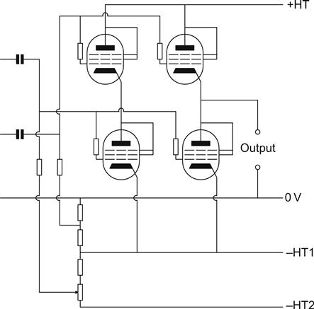
The Quad II
The Quad II is an unusual design, which at first sight does not look too promising, but works because the design is synergetic.
In this design, not only has the phase splitter been combined with the driver stage, but it has also been combined with the input stage. In order to achieve the necessary gain, pentodes have been used. Output resistance is therefore high, as is input noise. To make matters worse, a variant of the see-saw phase splitter has been used. The output stage has local feedback, requiring increased drive voltage (see Figure 6.25).
The output stage is a pair of KT66 beam tetrodes with anode and cathode loads split in the ratio 9.375:1. The cathode connection, therefore, provides little drive to the loudspeaker and may be considered to be series feedback from the output transformer. However, the cathode current in the output transformer is the sum of the anode and g2 currents, and it was found that this summation reduced third harmonic distortion by a further 8 dB over that due to the negative feedback [13].
The effect of this transformer-coupled feedback on output resistance is the opposite to what might be intuitively expected [14]. If we simply leave a cathode resistor unbypassed, then this generates series feedback which increases ra, yet transformer-coupled feedback reduces ra. This can be understood if we apply a short circuit as a load. Clearly, the output stage is unable to drive any voltage into this load, but conversely there is no feedback signal applied to the cathodes. The grids are therefore driven by the full input signal, rather than the input signal minus the feedback, so the output stage is driven harder as it attempts to maintain its voltage into a short circuit. This action is directly equivalent to reducing output resistance, and the new value of output resistance can be found using the normal feedback equation.
The transformer primaries are equivalent to 3 kΩ anode to anode. With tetrodes, this low value of anode load results in a reduction of third harmonic distortion, and an increase in second harmonic, which is then cancelled by push–pull action in the output transformer (assuming that the output valves are perfectly matched).
The automatic bias is shared, so there is no provision for balancing anode current, and we can expect an increase in distortion at low frequencies due to saturation of the (rather small) transformer core. Curiously, the cathode resistor was only rated at 3 W, yet it dissipates 3.8 W. If your Quad II distorts, a burnt-out cathode bias resistor may well be the cause.
Even with pentodes, there is not a great deal of gain from the driver circuitry, and input sensitivity is low: 1.4 V for full output. This is an excellent choice of input sensitivity for a power amplifier, as not only does it guarantee impeccable noise performance (even from a pentode), but also it means that the input is far less susceptible to hum and noise from input cables or heater circuitry. The Quad II was only beaten in signal-to-noise performance by the Williamson, which was quieter because it had a triode input stage.
Despite being a variant of the see-saw phase splitter, the phase splitter/input stage does not rely on feedback for balance, and its operation is quite elegant. The output valves must each have a grid-leak resistor, so instead of applying additional loading to the driver valves, a tapping is taken from one of these to provide the input for V2. Provided this tapping has an attenuation equal to the gain of V2, the output of the phase splitter must be balanced. Component variation means this will not always be true, so the cathodes of the two valves are tied together to improve balance.
Pentode stages have output resistance ≈RL. Since RL for the Quad input/phase splitter/driver is 180 kΩ, this would appear to be very poor at driving the ≈30 pF input capacitance of the output stage, resulting in a cut-off of ≈30 kHz. However, apart from the output transformer, this is the only High Frequency cut-off in the circuit, and it is not a problem because it is the dominant pole. Each output valve requires a swing of ≈80 Vpk–pk, which is easily provided, because pentodes can approach 0 V more closely than triodes, and also because LC filtering was used on the HT line, rather than RC filtering, thus increasing the available HT. The LC filtered HT supply also feeds g2 of the output valves, which has the valuable advantage of reducing hum, since the anode current of a tetrode or pentode is far more dependent on g2 voltage than anode voltage.
Pentodes need to have g2 decoupled to ground. Instead of each EF86 having a capacitor to ground, a single capacitor is connected between g2 of the two valves. This has three advantages:
• If we had two individual capacitors, they would effectively be in series, with a centre tap to ground. Since each valve is connected to an equal but opposite signal, the centre tap would be at ground potential even if it were disconnected from ground. Therefore, we could cheerfully disconnect the centre tap from ground, leaving two capacitors in series that can be replaced by a single capacitor of half the value.
• Since this one capacitor is connected between two points of equal potential, it doesn’t need the full voltage rating to ground. However, it is as well to consider the effect of fault conditions when determining the voltage rating, so this is not a great advantage.
• Connecting g2 of each valve together at AC helps maintain balance in the same way as commoning the cathodes.
Although substituting one stage that combines the functions of input, phase splitter and driver does not achieve the linearity of purpose designed stages, it achieves better linearity than the Mullard circuit because less gain is demanded from it.
With only a simple driver circuit and output stage within the global feedback loop, the elegant Quad II has no stability problems, but it has by far the smallest output transformer of all three amplifiers. A small output transformer always means compromised primary inductance, which means that much of the output stage’s available current is wasted driving the output transformer’s reactance rather than the external load. However, remember that the Quad II was designed to drive an electrostatic loudspeaker (open circuit at low frequencies), so this weakness was not apparent in its intended use.
New Designs
We have investigated individual stages, we have looked at functional blocks, and we have seen how classic designs were configured. Rather than merely observing, it is now time to put that knowledge to use, and design an amplifier.
In early editions of this book, it was suggested that an old amplifier could be cannibalised for its transformers and chassis. Sadly, this approach can no longer be justified because classic amplifiers are now likely to be fifty years old, and the amount of work expended in re-using components that might fail within ten years is prohibitive. It is now cheaper and easier to make an amplifier with completely new components.
Single-Ended Madness
There are three reasons why a single-ended design has been included:
• The author feels that the single-ended genre should be given a fair trial and hanging. Or not, as the case may be.
• The author was given an NOS 6528, and realised that not only could it form the basis of a stereo amplifier, but also he already had a suitable mains transformer, chokes, rectifiers, and HT capacitors. (The fact that a pair of custom-designed output transformers would be needed was not allowed to intrude upon this logic.)
• A single-ended amplifier is electrically simpler than push–pull, so it can make a good first project.
However, be warned. For a given output power, single-ended amplifiers are significantly bigger, heavier, and more expensive than push–pull.
The Scrapbox Challenge Single-Ended Amplifier
Unfortunately for the transformer manufacturers, much of the ironmongery for this amplifier came from the author’s salvage stock – hence the amplifier’s name. Almost none of the components are critical, although alternatives will be offered as the design argument progresses.
Choice of Output Valve
Power amplifier design starts with required output power, which then leads to the choice of output valve(s). Thankfully, loudspeakers are gently becoming more sensitive as their designers appreciate the advantages of a carefully chosen cone material, so even ≤10 W suffices perfectly well without having to resort to expensive high-efficiency designs such as horns. Having decided on ≤10 W, the next choice is which 300B to use. The world probably has enough 300B designs, so the 6528 made for an interesting alternative.
The 6528 (distributed by Tung-Sol/Chatham, Cetron, and Raytheon) is a double triode intended for use as a series-pass valve in regulated power supplies. The glass envelope and base resembles a GEC KT88, and it is internally akin to a 6080, but the detailed construction and consequent specifications are positively heroic (Table 6.3).
Table 6.3
Comparison of 6080 and 6528 Dual Triode Series-Pass Regulator Valves
| 6080 | 6528 | |
| μ | 2 | 9 |
| gm | 7 mA/V | 37 mA/V |
| ra | 280 Ω | 245 Ω |
| Pa(max) | 13 W | 30 W |
| Ik(max) | 125 mA | 300 mA |
| Va(max) | 250 V | 400 V |
| Ih | 2.5 A | 5 A |
| Cag | 8.6 pF | 23.8 pF |
| Cgk | 5.5 pF | 17.8 pF |
The primary attraction of the 6528 is its astonishingly low ra, which suggests that we could use a low-impedance output transformer – enabling better transformer design. We now need to decide what the primary impedance should be, so we will soon plot loadlines on the anode characteristics, but we must first clarify the class of output stage.
Choice of Output Class
Actually, there is very little room for manoeuvre. A single-ended amplifier can only be Class A. Class A2 implies grid current and requires power driving circuitry with extremely low output resistance, so this low-power amplifier will be Class A1, where no grid current is permitted, allowing a simple voltage driver stage to suffice.
Choosing the DC Operating Point by Considering Output Power and Distortion
A power valve consumes expensive heater power, so it does not make sense to operate it at any point other than its maximum anode dissipation (30 W). This means that our loadline must be a tangent to the Pa(max) curve. We also know that for maximum output, we should not clip one half of the waveform before the other, so our DC operating point must allow equal and opposite grid swings. Using the Tung-Sol/Chatham curves, sweeping a transparent ruler along the Pa(max) curve resulted in a 2 kΩ loadline with an operating point at Va=255 V, which required Vgk≈−27 V and Ia=120 mA (see Figure 6.26).
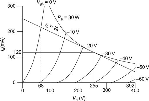
From the operating point, we can swing quite linearly to almost Vgk=0 V before drawing grid current, and to a roughly equal and opposite swing of Vgk=−50 V before cut-off begins to cramp the grid curves. Once we know how many grid volts can be swung, we can check the corresponding anode swing. At Vgk=−0 V, Va=68 V, and at Vgk=−50 V, Va=392 V, so the peak-to-peak anode swing is 324 V. If we assume that we swing an undistorted sine wave, then 324 Vpk–pk=115 VRMS.
The loadline passes from 500 V (Ia=0) to 250 mA (Va=0), which corresponds to 2 kΩ, and this is much higher than the conventional choice of 2ra. If we know the anode load and the voltage swing across it, we can calculate the power developed in the load to see if the proposed loadline is acceptable:
We can estimate the percentage of second harmonic distortion using:
At the chosen operating point, Vmax=392 V, Vmin=68 V and Vquiescent=255 V, resulting in 7.7% second harmonic distortion at full output.
This performance is typical for the genre, and other loadlines predicted significantly less audio power or worse distortion. (There is no point in being too critical about the anode load, since real loudspeakers are nothing like pure, constant resistances anyway.)