
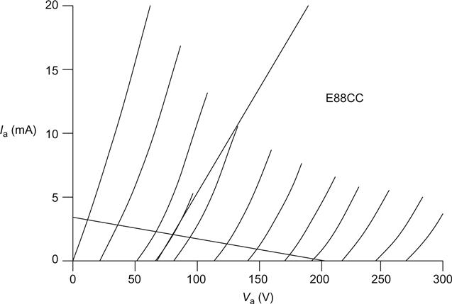
Plotting Va=204 V, Ia=0 mA is easy, but we don’t yet know where the other end of the loadline will be. However, we do know a point on the line; we know that Ia=2 mA at the operating point, although we do not know the voltage. It is up to us to choose a voltage, and Va=81 V is a good choice for linearity. Linearity is still important in a CCS because the complete circuit will probably modulate the sink’s anode voltage with an audio signal. If linearity is poor, this indicates non-constant ra, which is part of the term that governs the output resistance of the sink. If the output resistance varies with applied voltage whilst it is being used as an active load for another valve, it will cause distortion in that valve. If we now draw our loadline, we can find the current through RL when Va=0. From this, we can calculate the value of RL, which is then 60 kΩ. The nearest value to this is 62 kΩ, and this is what we would use.
Since Ia=2 mA, we know that the cathode of the valve will be at 124 V. Vgk=−2.5 V, so the grid needs to be at 121.5 V. This voltage is set in the normal way using the potential divider and capacitor combination.
The AC resistance, looking into the anode of this circuit, is:
For our design, this gives a value of slightly more than 2 MΩ. Achieving this result with a pure resistance would require a 4 kV HT supply. The AC resistance is in parallel with Cout, and Cag causes sink gain to fall, so the sink impedance falls as frequency rises. (Cout is the capacitance from anode to all other electrodes except the grid.)
Pentode Constant Current Sinks [8]
Pentodes are even better as CCSs because of their high μ, and are particularly useful when the allowable voltage drop across the sink is quite low.
If we needed a CCS of 10 mA, but were only allowed a 100 V drop across it, an E88CC could achieve an output resistance of only ≈100 kΩ, which is still a 10-fold improvement over a 10 kΩ resistor, but a pentode can do rather better.
If we leave even a 2 kΩ cathode resistor unbypassed, a pentode can increase its output resistance to >10 MΩ. This is a stunningly good CCS, but it should be remembered that pentodes tend to be noisy, so this would not be a good choice in the first stage of a sensitive pre-amplifier (see Figure 2.35).
When using a pentode as a CCS, it is vital to remember that the cathode resistor passes not only the desired constant current, but also the g2 current. Note also that the g2 decoupling capacitor must be taken to the cathode, and not to ground. This is because we want cathode feedback to increase ra, but we do not want the voltage between g2 and the cathode to vary, as this would cause positive feedback that would reduce ra.
Some pentodes make better CCSs than others because their anode characteristics are flatter, giving a higher output resistance, or because the flat part of their anode characteristics swings closer to 0 V. Table 2.1 shows single pentodes that are particularly suitable in CCSs.
Table 2.1
Comparison of Pentode Suitability versus CCS Current
| Type | Optimum current (mA) | Cout (pF) | Pa (W) |
| EF91/6AM6 | ≤6 | 3.1 | 2.5 |
| EF184/6EJ7 | 8–15 | 3 | 2.5 |
| EL83/6CK6 | 15–30 | 6.6 | 9 |
| EL822 | 20–45 | 6 | 12 |
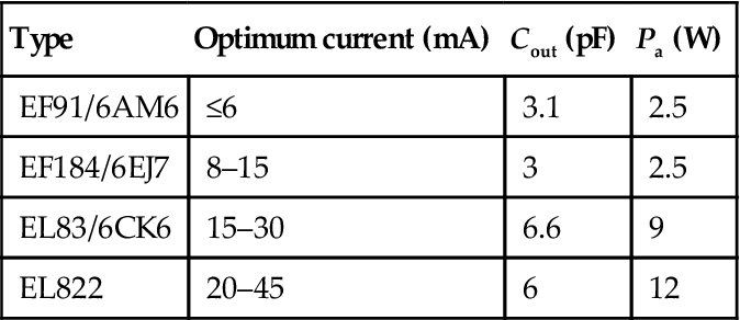
Table 2.1 shows optimum currents much lower than Ia(max), partly because at higher currents the anode curves tilt away from the horizontal, indicating reduced ra, but mostly because the major contribution to output resistance actually comes from the unbypassed Rk, whose value is multiplied by a factor of gm·ra(μ), which is typically 1,000 or more for a pentode. Higher currents require less bias and a reduced value of Rk, thus reducing output resistance. For maximum output resistance, it is better to use a valve with an oversized Pa, requiring a large Rk, than that with a perfectly rated Pa, requiring a smaller Rk. Unfortunately, the disadvantage of a CCS operated at very low Ia is that ![]() becomes a significant proportion of Ik, making the circuit inefficient.
becomes a significant proportion of Ik, making the circuit inefficient.
As an example, we might require an 8 mA CCS. However, this is the lower end of efficient operation for an EF184, and the curves show that it is likely to require ![]() , which means that total HT current has been increased by ≈38%. If there is only one sink, then this isn’t a problem, but if there are many such sinks, this can greatly increase the cost of the HT supply. If we were willing to reduce the sink current to 6 mA, this would bring it within range of the EF91, which only requires
, which means that total HT current has been increased by ≈38%. If there is only one sink, then this isn’t a problem, but if there are many such sinks, this can greatly increase the cost of the HT supply. If we were willing to reduce the sink current to 6 mA, this would bring it within range of the EF91, which only requires ![]() in this instance, reducing HT current from 11 mA to 7.55 mA. Although the EF91 does not have quite such attractive curves as the EF184, it is far cheaper to use, and if HT current is limited, it can be worth bending a design to allow its use.
in this instance, reducing HT current from 11 mA to 7.55 mA. Although the EF91 does not have quite such attractive curves as the EF184, it is far cheaper to use, and if HT current is limited, it can be worth bending a design to allow its use.
Optimally biassed, most small-signal pentodes split Ik between Ia and ![]() by ≈4:1 ratio. Thus, 8 mA of Ia typically requires 2 mA of
by ≈4:1 ratio. Thus, 8 mA of Ia typically requires 2 mA of ![]() . It is very important to check that the pentode’s Ia, Pa, and especially
. It is very important to check that the pentode’s Ia, Pa, and especially ![]() are not exceeded. Successful design of pentode CCSs requires full datasheets with curves or a valve tester/rig to allow voltages to be imposed and currents to be determined experimentally (which is more reliable).
are not exceeded. Successful design of pentode CCSs requires full datasheets with curves or a valve tester/rig to allow voltages to be imposed and currents to be determined experimentally (which is more reliable).
If the CCS is to be used in a stage with a low signal level, it is worth considering hum and screening. The EF184 has an integral metal screen, the EF91 has a conductive paint screen on the inside of the envelope, but the EL83 and EL822 power valves are completely unscreened.
The Cathode Follower with Active Load
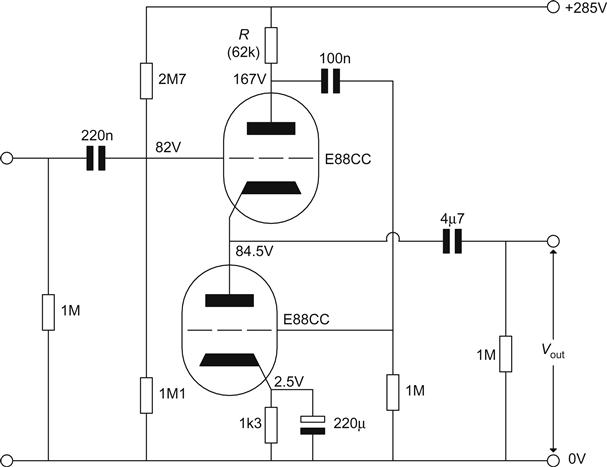
You probably have realised that the requirements for the triode CCS were set by the cathode follower designed earlier, so we can now combine them to form a cathode follower with an active load (see Figure 2.36).
Because the value of RL for the upper stage is now so large, the gain becomes:
The gain is, therefore, 0.97, which is only a little higher than before, but the distortion is greatly reduced. It is possible to make distortion predictions, but these are of very doubtful value, since real valves do not behave in the nice mathematical fashion that the equations require to generate sensible answers.
Grid current can cause a cathode follower to have very much higher distortion than expected. The author tested a self-biassed cathode follower using a 6S45 with an EF184 CCS active load, and then determined its input resistance by measuring the relative loss when driven from a 1 MΩ source resistance compared to 5 Ω. Sadly, the input resistance was not quite as high as predicted, and adjusting the value of grid-leak resistor from 150 kΩ to 1 MΩ not only changed the input resistance and slightly changed Ia (indicating grid current), but also reduced the distortion at +20dBu from 0.23% to 0.052%. Reducing the source resistance from 1 MΩ to 24 kΩ further reduced the Total Harmonic Distortion +Noise (THD+N) from 0.052% to 0.02%. Cathode followers are often used as buffers after volume controls, so this sensitivity to source resistance can be significant, particularly because, as we will see in Chapter 7, that some volume controls have higher output resistance than others.
To sum up, a carefully designed cathode follower with a resistive load produces low distortion – replacing this with an active load improves it further, and challenges test equipment, but for optimum distortion the valve should be selected/tested for low grid current.
The White Cathode Follower
Named after its inventor, the White cathode follower [9] is the basis of all output transformer-less (OTL) power amplifiers because of its low output resistance. The circuit comes in two forms: one self-contained and the other requiring an external phase splitter.
Analysis of the Self-Contained White Cathode Follower
The lower valve is fed with a signal from the upper valve, which, in turn, it feeds back into the cathode/grid circuit of the upper valve. At the input to the lower valve, the circuit may be considered to be a cascode amplifier (see Figure 2.37).
Provided that μ is reasonably large and the cathode is bypassed:
And the resistance looking into the cathode of the upper valve is:
But the gain of the lower valve is devoted to reducing the output resistance at the cathode of the upper valve, so combining the two equations gives:
μ is usually rather greater than 1, even for power triodes, so if we substitute μ=gm·ra:
We can now recognise the R·ra term as the inverted parallel combination of R and ra. This is significant because it indicates that there is a point beyond which increasing R has no effect and that final output resistance is limited by ra:
where
It should be noted that two rather dubious approximations were made to derive this result, both of which relied on high μ. The example in Figure 2.36 was optimised for low output resistance, and R≈10ra, beyond which limit no practical improvement is possible.
Although superficially completely different, the self-contained White cathode follower and the shunt-regulated push–pull (SRPP) amplifier described later in this chapter are both shunt-regulated amplifiers because both valves contribute to the AC load current. Rigorous equations for gain and output resistance derived by Amos and Birkinshaw [10] are as follows:
where V1 is the upper (amplifying) valve and V2 is the lower (regulating) valve.
Using an E88CC as an example, with gm≈5 mA/V and μ≈28, the rigorous equation predicts rout=6.6 Ω, whereas the approximate equation is only 4% high at 6.9 Ω despite the two dubious approximations. Experimentation with a spreadsheet reveals that this version of the White cathode follower is unsuited to low-μ valves, since a 6080 (μ=2) predicts rout≈35 Ω, which is worse than when used as a standard cathode follower (rout≈15 Ω). However, a triode-strapped E55L (μ=30) predicts rout<2 Ω, and a triode-strapped D3a (μ=80) should easily achieve rout<1 Ω. It is easy to become excited about predicted low output resistances, but we must always remember that all such equations contain the implicit assumption that the output resistance of the HT supply is 0 Ω, which is normally only approximated by a regulated supply.
Since the White patent suggested that the circuit was particularly suitable for driving analogue video cables (which were typically 75 Ω transmission lines), it is not surprising that the stage makes an excellent output cable driver for a pre-amplifier.
Note that because the feedback that causes the low output resistance is AC coupled, output resistance rises at low frequencies not to 1/gm, but to:
In this instance, rout rises to 1.5 kΩ, rather than 200 Ω, which is what a normal cathode follower would achieve. The practical implication is that the stage will not short circuit low-frequency noise (such as mains hum) induced into the output cable as effectively as a stage with a true 6 Ω output resistance from DC to light.
Usually, we do not need to calculate the gain Av precisely, and the general cathode follower approximation of Av=μ/(μ+1) is perfectly adequate, but if the stage was to be used as the basis of a Sallen & Key filter, the rigorous calculation of gain might be needed.
The White Cathode Follower as an Output Stage
The primary use of the White cathode follower is as an output stage for OTL amplifiers. A series resistor in either of the HT rails is a serious waste of power, so we must use the version preceded by a phase splitter (see Figure 2.38).
Assuming that neither valve switches off under any signal conditions (Class A), the gain of the lower valve is:
The upper valve no longer has a resistor in its anode circuit, so rk=1/gm, and this is the anode load of the lower valve. Substituting:
Multiplying by gm and simplifying:
A cathode follower with Rk=∞ would have the same gain, and because the lower valve strives to produce exactly the same signal as a standard cathode follower if it saw Rk=∞, there is no voltage difference between the two valves, so the upper valve does see Rk=∞. However, the input to the lower valve must be inverted, requiring an external phase splitter.
The lower valve no longer reduces the output resistance of the upper valve, since with a gain of 1 it cannot apply feedback to the upper valve, which is why OTL amplifiers need considerable global feedback to bring their output resistance down to a suitable value for damping moving coil loudspeakers.
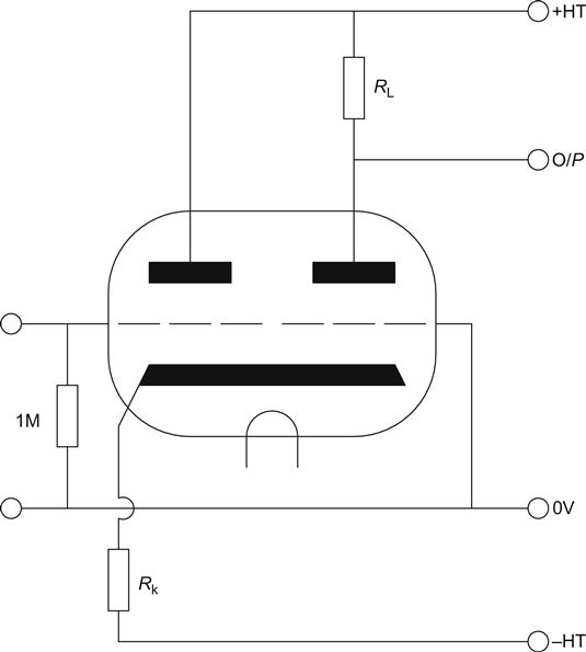
The μ-Follower
Invented by J.W. Horton [11] in 1933, but forgotten, this is a design which has attracted considerable interest since its rediscovery a few years ago [12]. (There is nothing new under the sun.) Essentially, it is a common cathode amplifier with an active load. Unlike the cathode follower, where it is arguable whether this is really necessary, the common cathode amplifier can definitely benefit from this sort of treatment (see Figure 2.39).
The top valve is a self-biassed cathode follower that has its input capacitively coupled from the anode of the common cathode lower stage. Since the cathode follower has Av≈1, and is non-inverting, the signal at its cathode will be nearly equal to that at the anode of the lower valve. If this is the case, then there will be little, or no, signal voltage across the upper resistors. Little, or no, signal current flows, implying a high-resistance active load or constant current source. The lower valve achieves voltage gain Av≈μ, and it produces low distortion (ra is no longer a factor). As a bonus, we have two output terminals, either the direct output from the lower anode or the low resistance output from the cathode follower. It should be noted, however, that the high-resistance active load actually only operates at AC, since the coupling capacitor forms a high-pass filter in conjunction with the (admittedly high) cathode follower input resistance.
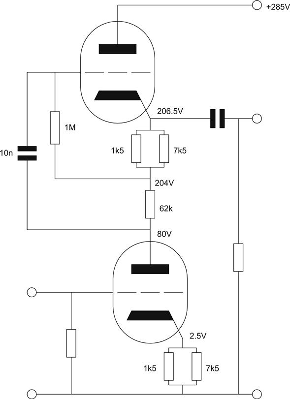
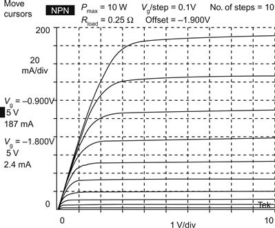
If the upper valve is a constant source (even if only at AC), then we can plot the loadline for the lower valve as a horizontal line (see Figure 2.40).
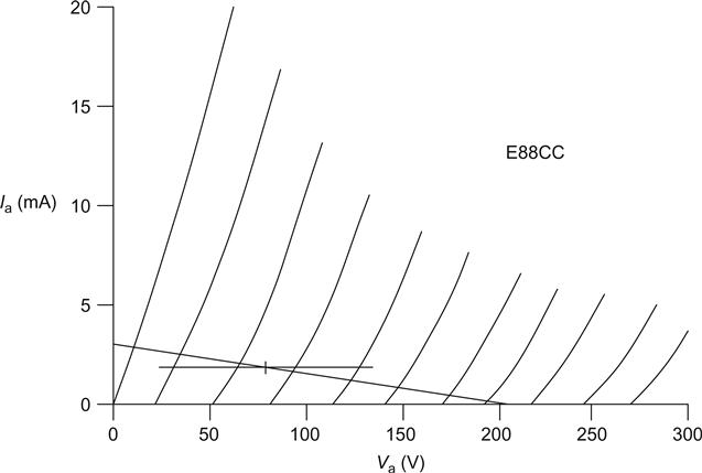
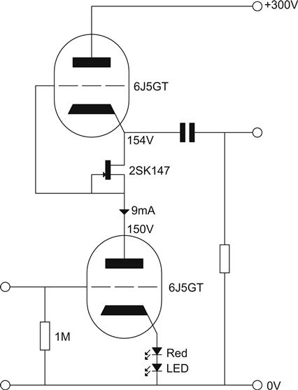
This is an example of an AC loadline, where the slope of the loadline does not relate to DC conditions, although it must pass through the DC operating point. We can move this line to any operating point that we like. If we choose an anode current of 2 mA, and bias the anode voltage to 80 V, this gives μ=32.5, and so we would expect a gain of ≈32.
We now have to determine the operating point for the upper stage. We will supply the compound stage from an HT of 285 V, leaving 205 V for the upper stage. Since the anode currents are equal, Ia for the upper valve must also be 2 mA. If we now choose an anode voltage for the upper valve (I have chosen 80 V), we can plot the loadline. At Va=0, we have a current of 3.25 mA, which corresponds to a 63 kΩ total cathode load for the upper valve. Vgk for the upper valve is 2.5 V, for Ia=2 mA; we need a 1.25 kΩ cathode bias resistance (1k5//7k5). We have now established the DC conditions of the stage.
Once we know the gain of the cathode follower, we can determine the value of the active load that it presents, and find its input resistance, which will enable us to choose an appropriate value for the coupling capacitor.
From the loadline, the gain before feedback is 29, so the gain of the cathode follower is 29/30, which is 0.97. The lower valve sees an anode load of:
This gives a value of ≈2 MΩ, so our earlier assumptions about the gain and linearity of the lower stage were justified. We can use our earlier formula to determine the input resistance at the grid of the cathode follower:
This gives an input resistance of ≈19 MΩ. If we need a 1 Hz cut-off, then 10 nF is perfectly adequate. The cathode bias resistor for the lower valve is calculated in the normal way.
The lower valve’s ra and stray capacitance form a low-pass filter, and although this effect is generally negligible with medium-μ valves such as the 6J5, it becomes significant when high-μ valves such as the 7F7 are used. There are two ways in which we can inadvertently raise ra and cause significant High Frequency loss:
• For high-μ valves in particular, the choice of operating point is a balance between maximum swing (requiring low Ia, but causing high ra) and High Frequency f−3 dB point (low ra, but requires high Ia).
• Although the high value of load resistance for the lower valve causes β to be so small that not bothering to bypass the lower cathode resistor in a μ-follower doesn’t cause noticeable loss of gain at 1 kHz, it raises ra.
As an example of these points, a μ-follower using a 7F7 as the lower valve suffered 0.9 dB loss at 20 kHz due to the interaction between excessive ra and stray capacitances when the cathode bypass was removed (1 kHz gain was unchanged).
An extremely useful secondary advantage of the μ-follower is its excellent immunity to noise on the HT supply, known as Power Supply Rejection Ratio (PSRR). At the output of any common cathode amplifier, PSRR can be found:
This is quite simply because ra forms a potential divider with RL. For maximum rejection of HT noise and ripple, RL should be as high as possible compared to ra.
A pentode has ra>RL and, therefore, has no rejection of HT noise.
Cathode feedback considerably increases ra, but does not reduce total gain by a proportionate amount and, therefore, destroys HT rejection. In our (bypassed) example, ra for the lower valve is equal to 6 kΩ and the active load ≈2 MΩ, resulting in 50 dB rejection of HT noise, but removing the bypass would raise ra for the lower valve to 47 kΩ and reduce HT rejection to 33 dB, despite leaving gain relatively unchanged.
Strictly, we should include the loss of the cathode follower in any calculation of gain to the low resistance output (Atotal=μ×Acathode follower), giving a gain of 31.5 in this instance.
The Importance of the AC Loadline
Up until now we have tacitly assumed that the input resistance of the following stage had little, or no, effect on the performance of the preceding stage. This would not be true if we used the anode output of the μ-follower because the value of the following grid-leak (typically ≈1 MΩ) is not merely comparable with the value of RL, it is actually less than RL and, therefore, lowers the effective value of RL from ≈2 MΩ to 670 kΩ. This has a negligible effect on gain, but trebles the distortion, so using the anode output is not recommended.
Whilst Rg≥10RL, it is legitimate to ignore its effect on the preceding stage, but once it becomes smaller than this, we should consider drawing an AC loadline to investigate whether it will cause a problem. Stages with active loads must take into account the input resistance of the following stage.
An accurate AC loadline is easily drawn. First we find the AC load, which is usually just the anode load and the following grid-leak in parallel. We know that the AC loadline must pass through the operating point, so all we need is a second point. The simplest way to do this is to move a convenient number of squares horizontally (change the voltage by 100 V or so), and calculate the increase, or decrease, in current through the AC load to give our second point. The line through these points is then the AC loadline, so inspection of this line gives the gain and linearity of the stage including the effects of the following load resistor.
Upper Valve Choice in the μ-Follower
There is no reason why the upper valve should be the same as the lower valve in a μ-follower. As a rule of thumb, the AC load resistance seen by the lower valve can be found by:
Maximising rL minimises distortion in the lower valve, but experiment shows that once rL≥50ra, there is no further benefit to be gained and it is more profitable to investigate the distortion produced by the upper valve. Because a cathode follower operates with 100% feedback, increasing μ increases feedback and reduces distortion. However, high-μ valves need a higher value of Va to avoid grid current, reducing available Va for the lower valve and lowering maximum voltage swing.
High gm is also useful in the upper valve if the stage is to feed a passive equalisation network because the resultant low (but changeable) rout is a smaller proportion of the network’s series resistance.
The 6545P single triode has μ=52 and gm≈20 mA/V at sensible anode currents, but its main advantage as the upper valve is that it can swing Vgk close to 0 V without distortion, allowing a high output voltage swing from a given HT voltage.
When triode strapped (g2, g3 to a), the D3a pentode is also a good choice as μ=80, and gm≈20 mA/V is easily achievable even at quite low currents, but significant grid current begins at Vgk≈−1.1 V. The D3a has gold-plated pins and was produced in the era when gold plating genuinely meant special quality. Not only does it meet its published specification, but it is very consistent from one sample to another. By contrast, the (Soviet era) 6545P generally only just meets the lower limits of its specification and is rather variable, although its anode curves are extremely linear.
Limitations of the μ-Follower
Although the μ-follower is an excellent gain stage, it does have limitations. We have seen that it has a low output resistance and low distortion, and it is, therefore, tempting to use it as a line stage to drive long cables or low input resistance transistor amplifiers.
However, a low-impedance load steepens the AC load line of the cathode follower upper valve. Although this valve has 100% feedback, the steeper load line slightly reduces gain and the cathode follower can no longer bootstrap the lower stage’s RL as effectively, so the lower valve sees a reduced load resistance, and distortion in the lower valve rises; connection of an external load always increases distortion within a μ-follower. As an extreme example, the rout of a 6J5/6J5 μ-follower was tested at 0 dBu. At +28 dBu, the stage produced 0.29% THD+N, so it was predicted to produce ≈0.01% THD at 0 dBu. However, an output resistance measurement that dropped the output from 0 dBu to −6 dBu by loading it with a 720 Ω resistance increased THD+N to 0.85%.
If a low-load resistance must be driven with minimum distortion, the μ-follower can be buffered by a cathode follower. To drive the load effectively, the cathode follower should pass ≥10 mA, and the valve should be a frame-grid type with high gm and high μ; 6545P and triode-strapped D3a are ideal. The cathode follower is a high-impedance load, so it can be direct coupled to the lower output of the μ-follower to avoid the inevitable distortion of the upper valve in the μ-follower. For lowest possible distortion, the cathode follower should have a CCS as its load.
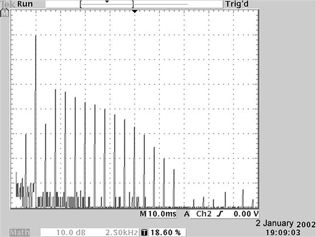
A well-designed μ-follower enters overload very suddenly. A 6J5/6J5 μ-follower driven from a 51 kΩ source was driven into grid current, resulting in an output of +38.1 dBu (61.6 VRMS) at 0.87% distortion. A high source resistance causes hard clipping at the onset of grid current, so we should expect a decaying series of odd harmonics. However, because grid current only clips one half-cycle and asymmetry causes even harmonics, we can expect all possible harmonics (see Figure 2.41).
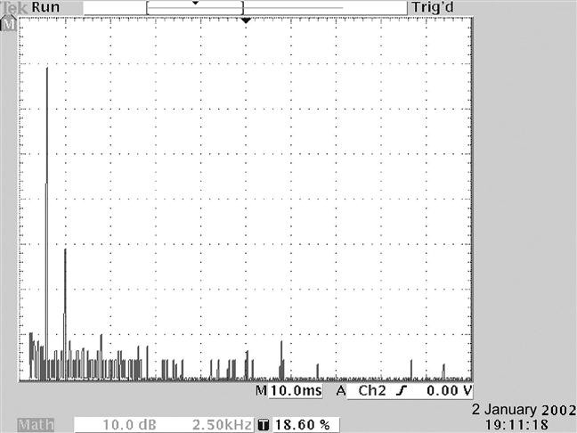
Dropping the level by 1 dB to +37.1 dBu reduced the distortion to 0.54%, and the higher harmonics entirely disappeared (see Figure 2.42).
The μ-follower is a gain stage and cathode follower connected in such a way that it provides a CCS load to the gain stage, making it much more linear. The downside is that the cathode follower is in series with the gain stage and consumes excess HT voltage because the (normally triode) cathode follower cannot swing to Va=0, and also because of the voltage dropped across RL. If we don’t combine the two valves in this way, but instead use a semiconductor CCS load for the gain stage and another for the (DC-coupled) cathode follower, we can obtain the same distortion as the μ-follower but a higher maximum output swing for a given HT voltage. We will investigate semiconductor CCSs at the end of this chapter.
The Shunt-Regulated Push–Pull Amplifier (SRPP)
Patented by RCA [13], the SRPP was developed in the early 1950s to be used as a power amplifier or modulator in television transmitters, where it was typically required to drive 1,100 Vpk–pk into a load of 400 Ω in parallel with 500 pF with low distortion [14]. Far more distortion can be tolerated in video than in audio, and the standards of video at the time were comparatively poor, so ‘low distortion’ meant ≈2% and ‘negligible distortion’ meant <1%.
Although we are unlikely to use the SRPP in its original application, it is useful to understand the problems that the transmitter engineers faced and how they were solved. Developing 1,100Vpk–pk across 400 Ω wasn’t really a problem – it just needed a large valve, but maintaining that voltage across the 500 pF capacitance was. The highest frequency produced by the 405 line ‘high definition’ system was 3 MHz, and at this frequency, XC≈100 Ω, requiring considerably more current than the 400 Ω resistance. The obvious solution was to increase the standing current in the stage, but this would have been wasteful of electricity because full amplitude High Frequency signals are very rare in real pictures (as opposed to test signals). What was needed was a means of sensing when the extra current was required, and then allowing a second valve to furnish that current. A resistor in series with the output of the lower valve senses the load current, so the voltage across this is used to drive the regulator (upper) valve. Because the regulator valve could typically quadruple the total signal power of the stage without requiring any additional standing current, this stratagem allowed a considerable increase in efficiency – a very important consideration in amplifiers dissipating kilowatts of heat.
The same type of valve is invariably used for both upper and lower sections (see Figure 2.43).
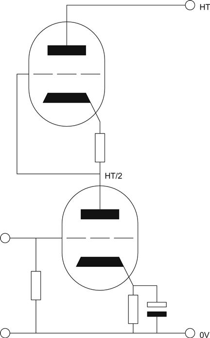
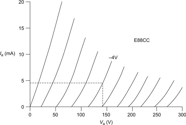
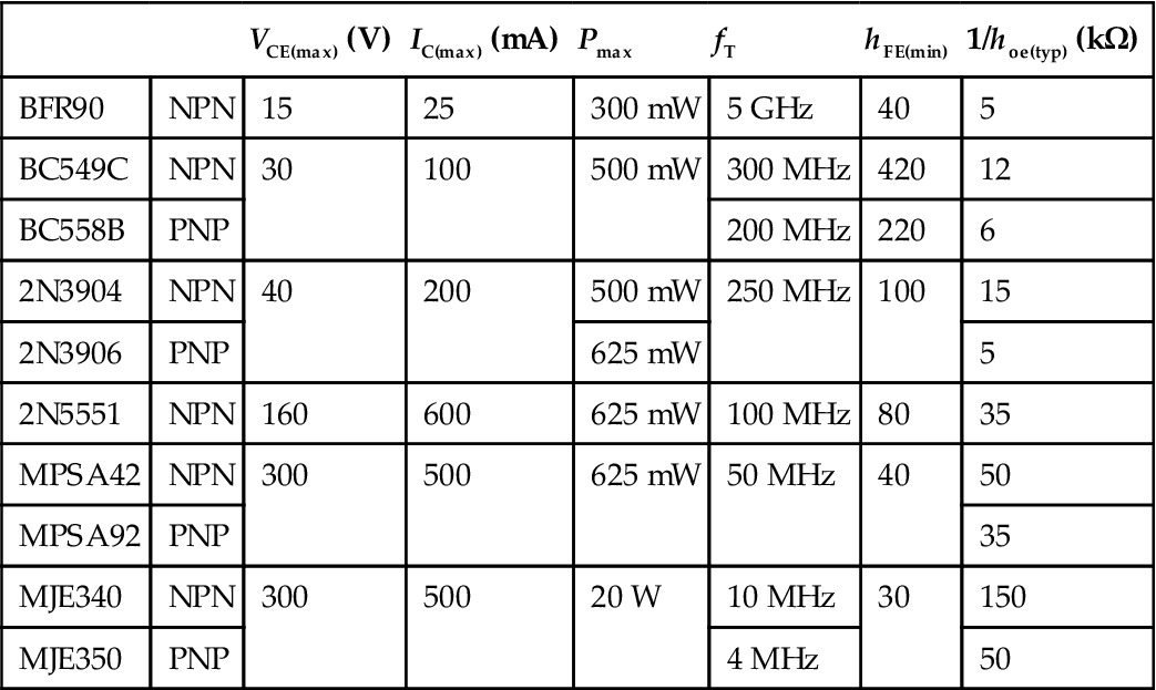
The same current passes through both valves, so the associated cathode bias resistor Rk is the same. From a DC point of view, the section above the lower anode is identical to that below it, so each section sees half the HT voltage. If we draw a vertical line on the anode characteristics at 285 V/2=142.5 V and choose our anode current, this determines the required bias. The −4 V curve crosses 142.5 V at 4.5 mA, so 4 V/4.5 mA=889 Ω, and a 910 Ω resistor is fine (see Figure 2.44).
Conceivably, differing valves or differing DC conditions could be used for upper (V2) and lower (V1) valves, in which case the full equations derived by Amos and Birkinshaw [15] give the gain of the stage as:
And the output resistance may be found from:
The SRPP is intermediate between the common cathode amplifier with a resistor as RL, and the μ-follower with an active RL, but the low value of upper cathode resistance Rk means that the value of RL seen by the lower valve is inevitably quite low, implying that the SRPP must have Av<μ and significantly increased distortion compared to a μ-follower.
A pair of typical 6J5GTs whose characteristics had previously been measured was set up as an SRPP:
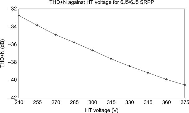
The equations predicted Av=14.3 and rout=2.3 kΩ. Measurement found Av=13.5 and rout=2.3 kΩ. The SRPP was compared with the μ-follower by swapping the same valves between stages, and testing with identical DC conditions for all valves. Unsurprisingly, given its heritage, not only did the SRPP deliver a significantly higher output voltage swing than the μ-follower, but also the μ-follower required a higher HT voltage because it wastes HT across its additional 10 kΩ Rk (see Figure 2.45).
At an output of +28 dBu (19.5 VRMS), the μ-follower produced 0.24% THD+N, but the SRPP produced 1.32%, an increase of 15 dB. As predicted, the SRPP produces significant distortion, and although this falls with level, it is still rather high for use in a pre-amplifier gain stage. The effect of HT voltage on distortion at +28 dBu was also investigated (see Figure 2.46).
Although the SRPP seems a poor choice compared to the μ-follower, it does have the advantage that it is DC coupled internally (the μ-follower needs a coupling capacitor to the upper valve), and it is, therefore, immune to blocking (see Chapter 3).
The β-Follower
The β-follower [16] seeks to exploit the advantages of the μ-follower with the efficiency and DC coupling of the SRPP stage (see Figure 2.47).
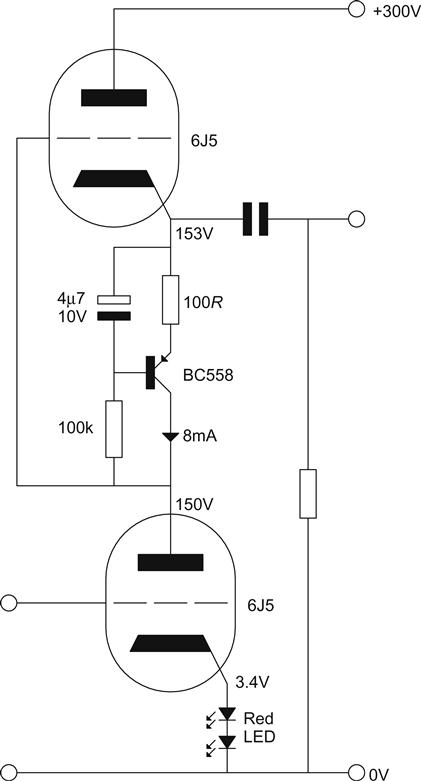
Replacing the cathode bias resistor with a bipolar transistor allows the large (perhaps 10 kΩ) RL to be discarded, reducing wastage of HT, and allowing the two valves to be DC coupled.
Bipolar transistors are usually treated as if their output characteristics are constant current, which implies horizontal output curves, but real transistors have curves that slope slightly (see Figure 2.48).
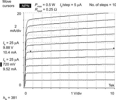
Looking into the anode, a valve multiplies Rk by μ; similarly, a bipolar transistor multiplies any resistance in the emitter circuit by β, or hfe, so the curves can be flattened by adding an emitter resistor. Since hfe for a small-signal transistor is likely to be ≈400, a 100 Ω resistor in the emitter makes the output resistance 1/hoe≈40 kΩ. The cathode follower then multiplies this resistance by its μ, perhaps 20, to give RL≈8 MΩ, which is even better than a μ-follower can achieve.
The β-follower easily achieves rL≥50ra, even with a low-μ upper valve, so the upper valve must be chosen for minimum distortion, otherwise it will compromise the excellent performance of the lower valve.
The β-follower is an excellent test bed for determining irreducible distortion. If the lower valve is fed from rs≈0, and loaded by rL≈∞, then the remaining distortion is due to errors in valve geometry, such as uneven grid winding. The 6J5/6J5 β-follower shown in Figure 2.47 gave distortion performance that challenged the author’s test equipment, with only the second harmonic being reliably measurable at −55 dB below the fundamental at an output level of +28 dBu – all other harmonics were better than −100 dB!
In theory, we could replace the bipolar transistor and its associated components by a depletion-mode junction field-effect transistor (JFET). If the gate is connected directly to the source, a typical 2SK147 becomes a ≈9 mA constant current source. However, rd (the output resistance looking into the drain) is typically <10 kΩ, so it is not as effective at reducing distortion as the β-follower (see Figure 2.49).
The Cathode-Coupled Amplifier
The cathode-coupled amplifier was a popular oscilloscope amplifier because directly coupling a cathode follower to a grounded grid stage produced a non-inverting amplifier having wide bandwidth; the circuit has recently become popular in OTL headphone amplifiers (see Figure 2.50).
The amplifier can be considered to be a cathode follower (non-inverting) coupled to grounded grid amplifier (also non-inverting).
The cathode follower has 100% negative feedback, and its gain before feedback is:
Feedback reduces gain:
Combining the two to give the gain after feedback:
Looking into the cathode of the grounded grid stage, we see:
But the cathode follower sees this rk in parallel with its load resistance Rk, so its gain becomes:
The total gain of the amplifier is the product of grounded grid gain and cathode follower gain:
As Tektronix [17] pointed out, once RL approaches ra (as would be likely in an oscilloscope) and μ is large, cathode follower gain simplifies to ½, implying a total gain roughly half that of a common cathode stage. Otherwise, provided that μ is reasonably large, the Rk term becomes negligible, and the gain simplifies to:
which is slightly lower than the gain we would expect from a conventional common cathode stage, but non-inverting.
The grounded grid section intrinsically has wide bandwidth because the control grid screens the cathode from the anode, and the cathode follower section has wide bandwidth because it does not suffer Miller capacitance from a changing anode voltage. Thus, the combined amplifier has wide bandwidth – which is why it was so popular as an oscilloscope amplifier.
However, there is a price to be paid for this bandwidth. Unless RL is very large, the load resistance seen by the cathode follower is only a few kΩ, which greatly increases its second harmonic distortion (H2). It is fortunate that the signal level at this point is likely to be low, because this load resistance causes very little gain before feedback and, therefore, very little feedback is available to reduce distortion. The increased H2 would not have been a problem in an oscilloscope because oscilloscope display tubes necessitated push–pull operation, which cancels H2.
The Differential Pair
All of the circuits that we have so far studied have been single-ended, which is to say that they have only one output. (The μ-follower-type circuits were single-ended because although they had two outputs, they were of the same polarity.)
By contrast, the differential pair has two inputs and amplifies the difference between them to provide two outputs, one inverted with respect to the other; this makes the differential or long-tailed pair [18] a very useful stage.
A differential pair can be made using the basic common cathode triode amplifier or with cascodes. (The μ-follower is not suitable because differential pairs attempt to exploit the normally large ratio between RL and Rk.) For simplicity, we will analyse the differential pair using the basic common cathode triode amplifier (see Figure 2.51).
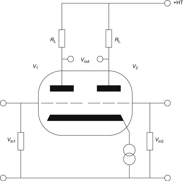
The circuit consists of two identical triodes, often in the same envelope, with their cathodes tied together, passing anode current to ground via a CCS and each driving equal value anode load resistors.
Suppose that we apply an input signal such that the voltage on the anode of V1 rises by 1 V. The current through V1 must, therefore, have fallen, but since both valves are sitting on a CCS, this can only occur if the current through V2 has risen by an equal amount. Since the anode load resistors are equal, it follows that the voltage on the anode of V2 must have fallen by 1 V.
The outputs of the two anodes are equal in voltage, but one is inverted with respect to the other.
Returning to the inputs: if we short circuit ![]() to ground, and apply a sine wave to
to ground, and apply a sine wave to ![]() , then the cathode will ‘follow’ that signal because, ignoring the anode loads, the circuit is a cathode follower. This means that V2 is driven by its cathode, an amplified signal appears on its anode, and, therefore, an equal and opposite signal appears on the anode of V1. The argument works in the same manner for a signal applied to
, then the cathode will ‘follow’ that signal because, ignoring the anode loads, the circuit is a cathode follower. This means that V2 is driven by its cathode, an amplified signal appears on its anode, and, therefore, an equal and opposite signal appears on the anode of V1. The argument works in the same manner for a signal applied to ![]() .
.
Gain of the Differential Pair
When driven by a signal connected between the two grids, the gain of the differential pair is identical to that of a standard common cathode stage, but the output voltage is found between the anodes of the stage. Therefore, if we look between one anode and ground, we only see half of the output voltage, and the gain appears to be halved.
If we use the differential pair as a phase splitter, and apply the same input voltage as before between one grid and ground, instead of each grid seeing half the input voltage, one sees the entire input voltage and the other none. Because the voltage difference between the two grids is the same, the gain remains the same.
Output Resistance of the Differential Pair
Provided that the output of the differential pair is not unbalanced in any way, rout at each terminal is identical to that of a simple common cathode amplifier (ra‖RL).
However, if only one output is loaded, the output resistance rises considerably. Working backwards from the path to ground (HT supply) via the first RL, we see:
But we now also see a path Rk to ground (0 V), which is in parallel with rk:
Multiplying through by (μ+1):
Looking down through the second anode, we see ra in series with this multiplied by a factor of (μ+1):
If we divide by Rk(μ+1), we obtain:
As Rk tends to ∞, the right-hand term on the bottom line reduces to zero, resulting in a maximum value of ![]() :
:
This high value of ra will become significant when we investigate the PSRR of the differential pair.
If RL>>ra, then the output resistance (only one terminal loaded) is:
AC Balance of the Differential Pair and Signal at the Cathode Junction
Provided that the anode load resistors are perfectly matched, the only way that there can be an AC imbalance at the anodes is if some signal current is lost to ground by a finite tail resistance. Thus, an infinite tail resistance would allow two entirely different valves to achieve perfect balance provided their anode loads were matched.
If the two valves are perfectly matched, then they must have identical gain to their identical anode loads and there can be no signal at the cathode junction (grids driven by signals of equal and opposite polarity). If they are not perfectly matched, their gains must differ, so there must be a signal at the cathode junction.
If the two valves are not driven by signals of equal and opposite polarity, there must be a signal at the cathode junction. This statement is easily understood by considering the extreme case of a phase splitter (signal at only one grid); the only way the valve with no signal on its grid can have its Vgk modulated is by moving its cathode, requiring a signal at the cathode junction.
The two previous statements show that any imperfection of drive or valve matching results in a signal at the cathode junction – there should ideally be no signal. Worse, if there is a signal, it implies that the valves are being forced to amplify that signal in order to produce their output signal, and any interference signal at the cathode junction will also be amplified.
Common-Mode Rejection Ratio (CMRR)
Rather than assuming signals of equal and opposite polarity on each grid, we will now consider the response to identical signals on each grid. If we apply +1 V to both grids, the cathode voltage simply rises by 1 V, the cathode current remains constant, and the anode voltages do not change, because we have not modulated Vgk. The amplifier only responds to differences between the inputs or differential signals. Applying the same signal to both grids is known as a common-mode signal.
This property of rejecting common-mode signals is significant, since it implies that the circuit can reject hum on power supplies, or common-mode hum on the input signal, so we will investigate it further.
The signal at each output can be expressed in terms of currents using Ohm’s law:
Each output will be an exact inverted replica of the other if i1=i2, provided that the two load resistors are equal. There are two main ways in which this nirvana may be eroded:
• If signal current is lost through an additional path to ground. A signal current i1 flowing down V1 out of its cathode must split, with some current being lost down Rk and the remainder flowing up into the cathode of V2, to become i2. However, if Rk=∞, no current can flow down Rk, and i1=i2. If μ1=μ2, and RL(1)=RL(2), then:
This indicates that we should use high-μ valves, and maximise the ratio of Rk to RL. As an example, an EF184 constant current source (rsink=Rk≈1 MΩ) and E88CC differential pair (μ=32) and RL=47 kΩ would have CMRR≈57 dB.
• Results from the above equation will be degraded if μ1≠μ2, or if RL(1)≠RL(2), or a combination of the two. With the easy availability of low-cost, accurate digital multimeters, mismatching of load resistors is avoidable, but matching the valves is harder. If μ1≠μ2, then:
which indicates that high-μ valves are still desirable, but that matching is important.
Because the simple equation for CMRR ignores mismatched valves, mismatched load resistors and stray capacitances, any predictions of CMRR>60 dB should be treated with caution. Nevertheless, it is handy for checking that your tail resistance Rk is sufficiently high to ensure that predicted CMRR>40 dB, since 40 dB is an easily achievable CMRR in practice.
Power Supply Rejection Ratio (PSRR)
Since hum and noise on the power supply line are a common-mode signal, they must also be attenuated by the CMRR. We might also expect the potential divider formed by ra and RL to give significant additional attenuation. However, at either terminal, the only path to ground is via the other anode and RL up to the HT supply, which is exactly the scenario we investigated when determining rout with only one output loaded, therefore:
And the attenuation of power supply noise (solely due to potential divider action) is thus:
If RL>>ra, we achieve the maximum attenuation of 6 dB! Our previous example (RL=47 kΩ and ra=4.95 kΩ) attenuates by 5.2 dB, and together with the 57 dB due to CMRR, PSRR=62 dB.
It is now well worth comparing the PSRR of the common cathode stage, μ-follower and differential pair (same DC conditions for the amplifying valve) (Table 2.2).
Table 2.2
Comparison of PSRR for Different Topologies
| Stage | PSRR (dB) |
| Common cathode (RL=47 kΩ) | 20 |
| μ-Follower (rL≈742 kΩ) | 44 |
| Differential pair (rsink≈1 MΩ) | 62 |
The differential pair is the best, and will remain the best, since an improved constant current source for the μ-follower could be adapted to become an improved CCS for the differential pair.
Knowing the PSRR enables us to design power supplies correctly because it gives an indication of the allowable hum on the HT supply.
For example, the second (differential pair) stage of a balanced pre-amplifier might need the 100 Hz power supply hum to be 100 dB quieter than the maximum expected audio signal. At this point, the signal has not received RIAA 3,180 μs/318 μs correction, so the level at 100 Hz is 13 dB lower than at 1 kHz. However, peak levels from LP are +12 dB compared to the 5 cm/s line-up level, so the maximum audio signal at 100 Hz is 1 dB lower than the 1 kHz calculated signal level at the anode (2.2 VRMS)=2 V. We want 100 dB signal/hum, but because 62 dB of this will be provided by the differential pair’s PSRR, we only need the hum on the power supply to be 38 dB quieter than 2 V, so we could tolerate 25 mV of hum on the power supply – which is easily achievable.
Semiconductor Constant Current Sinks
The differential pair demonstrated the need for CCSs, but the pentode CCS is profligate with HT voltage (although it is a good sink), and a differential pair with grids at ground potential would require a subsidiary negative supply for the sink of −100 V. This is often undesirable, so a solution is needed.
Unlike the original valve designers, we are in the fortunate position of being able to use transistors, and even op-amps, if we consider them to be necessary. This is a perfect example of where a transistor or two can be very helpful.
The simplest form of a transistor CCS is very similar to our triode version. The red LED sets a constant potential of ≈1.7 V on the base of the transistor. Vbe is ≈0.7 V, so the emitter resistor has 1 V held across it – irrespective of its resistance. We can, therefore, use Ohm’s law to determine the resistance required to programme a particular current:
Thus, if we need to sink 5 mA, we would need a 200 Ω programming resistor. The AC resistance looking into the collector is:
In this instance, a BC549C (hFE guaranteed>420 and 1/hoe≈12 kΩ) gives rout≈96 kΩ. Note that an expensive 2 W resistor is required to bias the LED (see Figure 2.52a).
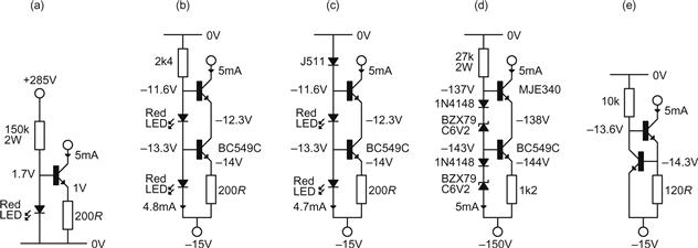
The simple circuit can easily be improved upon, and since silicon is cheap, it seems worthwhile to do so. There are two problems to be addressed. Firstly, the transistor needs VCE>0.5 V for it to operate as a CCS, which is uncomfortably close to typical bias voltages for high-μ valves such as the ECC83. Secondly, 92 kΩ output resistance is not especially high, and we can do much better.
A transistor cascode is broadly similar to a pentode, but a practical circuit requires a negative supply, although this may not be a problem in a power amplifier, because there is often a negative bias supply for the output valves that we can use. (Even though the bias winding normally supplies <1 mA, wire rated for 1 mA is very fragile, so transformer manufacturers typically use thicker wire, allowing us to draw 10 mA from this winding, and the increase in transformer VA loading is usually negligible.)
A cascode CCS has much higher output resistance than a single transistor CCS:
The AC output resistance of the initial design has been multiplied by the hfe of the second transistor (assumed to be 400), which improves it from ≈96 kΩ to ≈40 MΩ, and the value of 1/hoe (which we probably don’t know accurately) is now negligible.
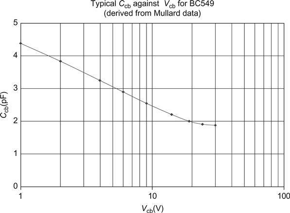
The qualities we want from a CCS are high output resistance and low output capacitance – because capacitance to ground reduces output impedance at high frequencies. All transistors have internal capacitance between their collector and base Ccb, and the higher the power and/or voltage rating of a transistor, the higher Ccb tends to be. Maximising performance at high frequencies means choosing the most fragile transistor we dare in order to minimise Ccb.
However, it is possible to accidentally make Ccb higher than expected (see Figure 2.53).
Ccb is the capacitance across the depletion region between base and collector, and its thickness is proportional to ![]() , so if there’s a choice between having 1 V and having 10 V across the transistor, choose 10 V – this is another justification for a negative supply. However, a more obvious advantage is that the negative supply allows the output port to be taken down to 0 V without linearity problems. High Frequency stability of the cascode CCS is excellent (see Figure 2.52b).
, so if there’s a choice between having 1 V and having 10 V across the transistor, choose 10 V – this is another justification for a negative supply. However, a more obvious advantage is that the negative supply allows the output port to be taken down to 0 V without linearity problems. High Frequency stability of the cascode CCS is excellent (see Figure 2.52b).
As shown, the cascode current sink is relatively sensitive to hum and noise on the negative supply because of current changes through the voltage reference. The cheapest and best solution is to regulate the negative supply, perhaps using a 337 three-terminal regulator, but if there isn’t enough negative voltage available for the 4 V drop needed across the regulator, a second-best solution is to insert a constant current diode into the chain that feeds the voltage reference (see Figure 2.52c).
The cascode CCS is easily adapted to withstand a larger voltage by replacing the outer transistor (the one connected to the load) with a higher-voltage type, but this generates two new problems:
• High-voltage transistors inevitably have a low hfe, and because rout is the product of the two current gains and the programming resistor, reduced hfe translates directly into reduced rout. Don’t over-specify the device – if you only need to withstand 100 V and dissipate 100 mW, then a 2N5551 (hfe(min)=80) doubles the output resistance compared to an MJE340 (hfe(min)=30).
• If the outer transistor has a significant voltage across it, it probably also dissipates significant power. As an example, 120 V×10 mA=1.2 W – which is too much for a small transistor, forcing an MJE340 and a heatsink. Elsewhere, the author has vilified small heatsinks on transistors, preferring to use the chassis as a heatsink, but this is the one instance where it is essential to use an individual heatsink. The collector of almost all power transistors is connected to the case, so we place an insulating washer between it and the heatsink. For an MJE340, the transistor, insulating washer and heatsink form a capacitance of ≈8 pF, and one end of this capacitor is connected to the output terminal of our CCS. If we connect the heatsink to ground, we connect 8 pF in parallel with the output of our CCS and reduce output impedance at high frequencies. Solution: Use an individual heatsink (oriented to lose heat efficiently), do not connect it to ground, and minimise its capacitance to ground.
Because we have voltage to spare, some of the lost output resistance can be recovered by setting a higher reference voltage, allowing a higher value of RE. The 1N4148 diode compensates for variation of the lower transistor’s Vbe due to temperature, but should not be added to LED references because the temperature coefficients of Vbe and VLED are quite similar, so they are already temperature compensated [19] (see Figure 2.52d).
It is essential to realise that it is only the outer transistor (the one connected to the load) that has to withstand any external high voltage. Not only is it unnecessary to use a high-voltage device for the inner transistor, but it would significantly degrade performance. High-voltage transistors always have low hfe − 40 is typical for the MJE340 – so a cascode CCS required to withstand +100 V using a pair of MJE340s would have an output resistance one-tenth that of exactly the same design using a BC549C as the inner transistor, simply because the BC549C has 10 times the hfe of an MJE340. Remember: choose the outer transistor to survive external conditions and the inner transistor to optimise performance.
The Williams [20] ‘ring-of-two’ circuit works by holding 0.7 V across the 120 Ω sense resistor. If that voltage rises, due to increased current through the resistor, T1 turns on harder, which causes the base voltage of T2 to fall. T2 begins to turn off, so the current through the 120 Ω resistor and, therefore, the sink current, is held constant (see Figure 2.52e).
Beware that because the ring-of-two relies on feedback applied over two transistors, there is a possibility of oscillation at high frequencies due to stray capacitances. By comparison, the cascode CCS is far less likely to become unstable.
Using Transistors as Active Loads for Valves
All the previous sink circuits can be mirrored about 0 V and PNP transistors substituted for NPN. If the circuit is then connected to the HT supply, all the previous sink circuits become constant current sources, allowing a triode to achieve Av=μ. More significantly, they permit a valve to achieve low distortion from a low HT voltage.
As an example, in common with all high-μ valves, the ECC83 needs considerable Va before it can be biassed out of grid current; 150 V is typical. As a general rule of thumb, RL>2ra, and as ra≈75 kΩ for the ECC83, we might use RL=150 kΩ. If Ia=0.7 mA, we would drop 105 V across RL, so we would need 255 V of HT. But we might only require the stage to produce an output swing of 5 Vpk–pk, so most of the HT is wasted. If we replace the 150 kΩ resistor with a constant current source, the valve sees a much higher value of RL, and we can set the HT voltage independently to accommodate the maximum required output swing (see Figure 2.54).
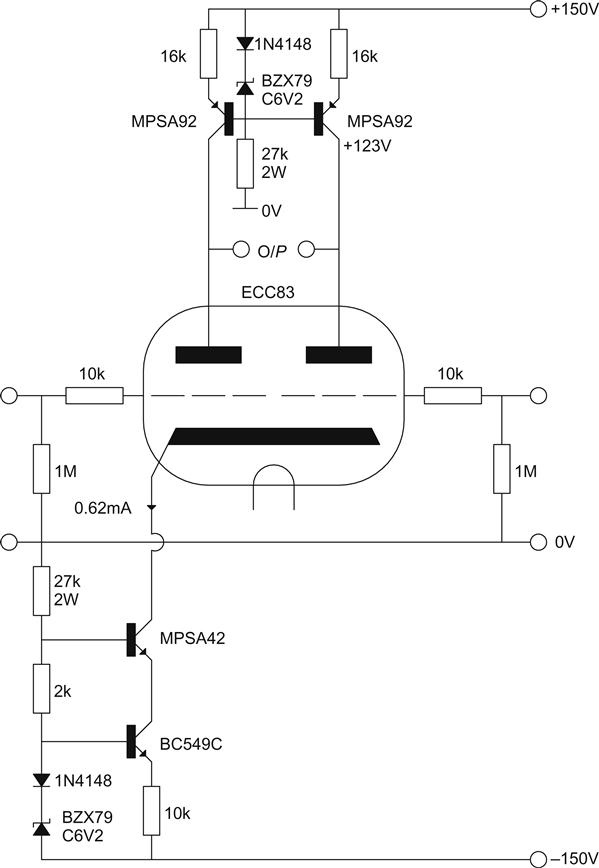
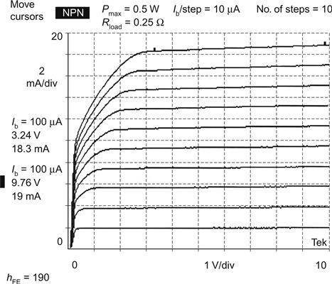
In Figure 2.54, the concept of operating a high-μ valve from a low HT was taken to the extreme because the author needed a high gain differential pair stage (ECC83: μ=100), but only had 150 V of positive HT available. Note that high-voltage transistors are required to withstand either anode swinging towards 0 V.
At fist sight, the circuit has two constant current sources, both trying to define the current in the same wire. The trick is that the cathode CCS is deliberately superior to the anode constant current sources, enabling it to enforce its behaviour upon them.
The anode constant current sources have an output resistance of ≈600 kΩ (hfe=40 and RE=15 k), but the cathode CCS has an output resistance of ≈130 MΩ (hfe1=420, hfe2=40 and RE=7k5). Thus, fine adjustment of the cathode CCS simply changes the voltage drop across the 600 kΩ output resistance of the anode constant current sources. The output resistance of the anode constant current sources doesn’t change appreciably with temperature, so the stability of the final circuit is down to the behaviour of the cathode CCS. The cathode CCS enforces 0.82 mA, ideally split equally between the anode CCSs so that each passes 0.41 mA. By Ohm’s law, a 1 μA change in current through the 600 kΩ output resistance of an anode CCS would cause a change in voltage drop of 0.6 V. The LED reference voltage and ordinary resistor in the cathode CCS circuit should be stable to <1% drift in current, resulting in <2.5 V drift in each anode voltage, which is perfectly acceptable.
Although Zener diodes are normally bypassed to reduce noise, the noise generated by both diodes is a common mode and is, therefore, rejected by the next (differential) stage. On test, the circuit achieved the required differential swing of 7Vpk–pk at 1 kHz with only 0.04% distortion.
A cascode greatly increases rout, flattening the loadline and reducing distortion in the valve. If we wanted to maximise output swing and minimise distortion, we might operate a 7N7 (loctal equivalent to 6SN7) at Ia=8 mA because μ becomes more nearly constant when Ia>6 mA. We assume that our cascode will provide a horizontal loadline, so we plot this at 8 mA (see Figure 2.55).
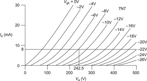
Normally, as Va rises, we have to consider the cramping of curves as Ia falls and cut-off is approached, but Ia is now a constant, and the only limit to positive swing is that the cascode requires sufficient voltage to operate correctly. 15 V is quite adequate for the cascode, so a 400 V HT would allow Va to swing to 385 V. Looking in the opposite direction along the 8 mA loadline, grid current is likely to begin at ≈100 V. The maximum possible swing is, therefore, 385−100 V=285 Vpk–pk≈100 VRMS.
Although the cascode forces Ia=8 mA, we must adjust valve bias to set Va. At just over maximum swing, we should clip positive and negative half-cycles equally, so the operating point should be halfway between the maximum and minimum permissible anode voltages – which is their average:
Looking at the curves, we see that Vgk≈8 V is required to set Va correctly, and this can be provided by an 8.2 V Zener diode (see Figure 2.56).
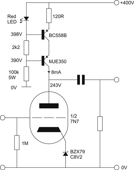
Since the stage is intended to swing large voltages, noise is not a problem, so it is not essential to bypass the Zener diode with a capacitor.
If there is 242.5 V across the valve, then there is 147.5 V across the lower transistor, so it must dissipate 1.18 W when quiescent. When Va swings to 100 V, the transistor must withstand 285 V at 8 mA, so it momentarily dissipates 2.28 W, and it might seem that this is the required rating of the transistor. However, the flat loadline has reduced distortion almost to zero, so the positive and negative swings are equal, and the average power dissipated in the transistor over one cycle of audio is equal to the quiescent power.
As before, it is only the transistor nearest the valve that must be able to withstand high voltages and dissipate significant power, so the additional transistor can be as fast and fragile as we like.
Optimising rout by Choice of Transistor Type
Table 2.3 compares transistors that are useful in support circuitry for valves.
Table 2.3
Abbreviated Data for Bipolar Transistors Useful in Valve Support Circuitry
| VCE(max) (V) | IC(max) (mA) | Pmax | fT | hFE(min) | 1/hoe(typ) (kΩ) | ||
| BFR90 | NPN | 15 | 25 | 300 mW | 5 GHz | 40 | 5 |
| BC549C | NPN | 30 | 100 | 500 mW | 300 MHz | 420 | 12 |
| BC558B | PNP | 200 MHz | 220 | 6 | |||
| 2N3904 | NPN | 40 | 200 | 500 mW | 250 MHz | 100 | 15 |
| 2N3906 | PNP | 625 mW | 5 | ||||
| 2N5551 | NPN | 160 | 600 | 625 mW | 100 MHz | 80 | 35 |
| MPSA42 | NPN | 300 | 500 | 625 mW | 50 MHz | 40 | 50 |
| MPSA92 | PNP | 35 | |||||
| MJE340 | NPN | 300 | 500 | 20 W | 10 MHz | 30 | 150 |
| MJE350 | PNP | 4 MHz | 50 |
VCE(max): The maximum allowable voltage between collector and emitter. (There are various ways of specifying this limit, so unless you know your precise circuit conditions, it is wise not to exceed 2/3 VCE.)
IC(max): The maximum allowable collector current.
Pmax: The maximum allowable power dissipation in the device (P=IC×VCE).
hFE(min): Minimum DC current gain from base to collector. (The author’s measurements suggest that hFE is generally double the manufacturer’s specified minimum value at the typical currents required by valves.)
fT: AC current gain hfe falls with frequency. At fT, hfe=1; this is known as the transition frequency.
1/hoe(typ): This is the typical AC resistance (equivalent to ra) seen looking into the collector. It is very rarely specified by manufacturers, so these figures were measured on a curve tracer at VCE=10 V and IC=10 mA to allow comparison between the types. PNP transistors tend to have a lower Early voltage than their NPN counterparts, so 1/hoe is lower and falls faster at higher currents.
Output resistance at low frequencies is partly determined by 1/hoe, but is dominated by hfe, since any resistance in the emitter circuit is multiplied by hfe. Impedance at high frequencies is shunted by the capacitance seen at the collector of the transistor, which will partly be determined by strays, but also by the transistor itself. In general, high-voltage/high-power transistors have a larger silicon die area, and greater capacitance, which is reflected in their lower fT. Additionally, fT varies significantly with IC, and operating a transistor below its optimum IC could reduce fT by a factor of five. If in doubt, download the transistor’s datasheet from the Internet – all the semiconductor manufacturers have excellent websites. As a consequence of these considerations, a small cascode CCS would ideally use two BC549Cs, or if low output capacitance (≈0.5 pF excluding strays) was essential and sufficient voltage was available, a triple cascode composed of a BFR90 with two BC549Cs beneath it. It is only critical for the outer transistor to have low output capacitance because the capacitances of the other transistors are at lower impedance points.
Any bipolar transistor needs a minimum VCE for it to operate linearly. For a low-voltage transistor at currents ≤30 mA, ≈1 V is sufficient, but higher currents may require 2 V (see Figure 2.57).
High-voltage transistors such as MPSA42 or MJE340 may require VCE>2 V. A CCS in a differential pair operating as a phase splitter has half the input signal across it, so this point can become significant. In a cascode sink, the lower transistor has hardly any AC signal across it, so it can operate with only 2–3 VDC, leaving the remaining DC for the upper transistor, which supports the bulk of the AC signal.
Field-Effect Transistors (FETs) as Constant Current Sinks
FETs are described as being depletion or enhancement mode. An enhancement mode device needs bias similar to a bipolar transistor to turn it on, whereas a depletion mode device needs bias similar to a valve to turn it off. Both can be used for making CCSs, but a depletion mode device can be self-biassed, whereas the enhancement mode device requires an external voltage, making it more cumbersome to use. ‘Constant current’ diodes are actually depletion mode FETs with their gate and source tied together. They tend to have a low maximum voltage, and disappointingly low slope resistance for their price.
As stated earlier, the output capacitance of any constant current circuit must be minimised if it is to maintain its performance at high frequencies, and that means choosing transistors with low output capacitance. Sadly, many high-voltage FETs simply aren’t suitable for valve electronics because of excessive output capacitance. As an example, the 700 mW power rating of the ZVN0545A suggests that it ought to be useful but it actually has higher output capacitance than the 15 W (TO220) DN2540N5. The reason for this is that semiconductor manufacturers make far fewer different devices than you think – they just package the dies differently. Thus, the DN2540N3 is the same silicon die, but in a TO92 package, reducing its power rating to 1 W.
Happily, the 400 V 15 W Supertex DN2540N5 depletion mode JFET is very nearly ideal for supporting valve audio. Unfortunately, the phrase ‘device variation’ was invented for FETs and never more so than for the voltage VGS(ID=0) required to turn the device on (or off); Supertex specify a spread of VGS(ID=0) from −1.5 V to −3.5 V. Fortunately, it’s easy to measure VGS for an individual device under any operating conditions, so devices can be matched or other circuit values can be determined for a specific device (see Figure 2.58).
The drain of the device is connected to a positive supply having the same voltage expected in the final circuit. The gate is connected to ground via a 1 kΩ gate-stopper resistor to prevent RF oscillation. The source is connected to a convenient negative supply via a programmable CCS adjusted to the required current. A Digital Volt Meter (DVM) connected between ground and source measures VGS. If we had more than one device, we would quickly run them all through the test jig to find each individual VGS. Devices with similar VGS would be deemed to be pairs.
Designing Constant Current Sinks Using the DN2540N5
The very simplest CCS using the DN2540N5 is little more than the contents of the constant current diode vilified earlier (see Figure 2.59).
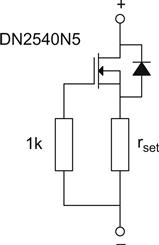
The carbon gate-stopper resistor prevents Very High Frequency (VHF) oscillation, and the source resistor programmes the current. Unfortunately, the value of the source resistor has to be found empirically for each DN2540N5, using the test jig of Figure 2.58. Alternatively, a variable resistor could be used and Adjusted On Test (AOT), but we still need to know the approximate value required in order to buy the correct value of variable resistor and if accidentally set to 0 Ω at switch-on, the saturation current might cause damage. It really is easier (and cheaper) to use the jig and fit a fixed resistor.
As an example, we might want to use a DN2540N5 as a CCS shared by the cathodes of a pair of EL84s. We know that when the EL84s are working, their cathodes will be at ≈11 V and will pass a total of 80 mA. The programmable CCS probably needs a minimum of 6 V across it to operate correctly, so we connect it to a negative supply of perhaps −9 V. We then apply +11 V to the drain of our Device Under Test (DUT), and using an ammeter adjust the programmable CCS to draw 80 mA through the DN2540N5. Having set the required current, we measure the voltage between 0 V and the FET’s source. (We don’t attempt to genuinely measure VGS on the FET because connecting a DVM to it will almost certainly cause oscillation, so we assume zero gate current and measure from 0 V.) Perhaps, we find that for our particular sample, VGS=−1.873 V at Ids=80 mA. All we need to do to turn the JFET into a 80 mA CCS for our EL84 is to add a source resistor that will drop 1.873 V when 80 mA passes through it (just like a triode), 1.873 V/0.08 A=23.4 Ω. The nearest standard value of 24 Ω will almost certainly do.
Like the pentode CCSs we investigated earlier, the FET multiplies the value of its programming resistor by μ. Unsurprisingly, μ is not given by the manufacturer, but can be found from the relationship:
The drain slope resistance rds can be found from the device curves by measuring output currents on one VGS curve at two widely spaced voltages (see Figure 2.60):
The mutual conductance gm at Vds=100 V can also be found from the device curves:
Note that although this value of gm is much lower than given on the datasheet, it is far higher than a valve could achieve at the same current. Combining the two values, we obtain μ≈4,500, which is a little higher than we might expect from a pentode. More significantly, a 39 Ω programming resistor in this FET would produce a ≈40 mA CCS having an output resistance of 175 kΩ. To put this into context, a genuine 175 kΩ resistor would drop 7 kV rather than 100 V and dissipate 282 W rather than 4 W.
The previous worked example was given not to suggest that such a process is needed, but to show just how good a CCS can be made with the DN2540N5.
Nevertheless, considerable improvement is possible, and like the simple bipolar transistor, the cascode is the way to go. Remembering how the single BJT CCS evolved into a cascode, we could add a voltage reference and second FET (see Figure 2.61a and b).

Unfortunately, by adding the voltage reference, we lose the very desirable property of the circuit being a two-terminal device. Because the DN2540N5 is a depletion mode device, the voltage reference is not strictly necessary, and we could use one DN2540N5 as the reference resistance for the other (see Figure 2.61c).
However, there are disadvantages because the lower device in the cascode is forced to operate with a very low Vds, but they can be ameliorated by returning the upper device’s gate stopper not to 0 V but to the source of the lower device (see Figure 2.61d).
This simple circuit is deservedly popular because (being two-terminal) it can be used equally well as an anode load or as the cathode tail resistance in a differential pair. The programming resistance is multiplied by both amplification factors, and even though the lower device’s performance suffers due to the low Vds, our previous example is likely to improve from ≈175 kΩ to ≈30 MΩ.
However, things are not quite as rosy as they might seem. The high resistance applies at DC, but not at AC because of output capacitance COSS [21] (see Figure 2.62).
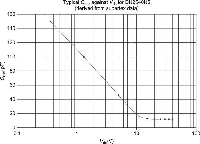
As can be seen from the graph, COSS is alarmingly high at low voltages and it is not until Vds>15 V that it falls to its asymptotic value of ≈12 pF. Fortunately, we would always operate at Vds>15 V (preferably 40 V, or more) because a BJT cascode is a better choice at lower voltages. An EF184 pentode CCS could achieve an output capacitance of 3 pF, but once we add typical strays of 3 pF to both circuits, the valve advantage degrades to 6 pF against 15 pF. This somewhat poorer output capacitance is the price we pay for the undoubted convenience of a two-terminal CCS.
The device has a maximum continuous current rating of 500 mA, so it should come as no surprise to learn that performance degrades at low currents. If you need a current <10 mA, then you owe it to yourself to see if there’s an alternative solution because the device is much better >10 mA, and at 25 mA it really comes alive (rout of a cascode CCS at 25 mA was four times that at 10 mA, all other factors kept constant).