
Circuit Analysis
Publisher Summary
This chapter illustrates Circuit Analysis. Electrons are charged particles. Charged objects are attracted to other charged particles or objects. Charged objects come in two forms—negative and positive. Unlike charges attract, and like charges repel. Electrons are negative and positrons are positive, but while electrons are stable in the universe, positrons encounter an electron almost immediately after production, resulting in mutual annihilation and a pair of 511 keV gamma rays. An electron is very small, and does not have much of a charge, so one needs a more practical unit for defining charge. That practical unit is the coulomb (C). One could say that 1 C of charge had flowed between one point and another, which would be equivalent to saying that approximately 6,240,000,000,000,000,000 electrons had passed, but much handier. Simply being able to say that a large number of electrons had flowed past a given point is not in it very helpful. One might say that a billion cars have traveled down a particular section of motorway since it was built, but if he/she were planning a journey down that motorway, he or she would want to know the flow of cars per hour through that section.
In order to look at the interesting business of designing and building valve amplifiers, we need some knowledge of electronics funmentals. Unfortunately, fundamentals are not terribly interesting, and to cover them fully would consume the entire book. Ruthless pruning is, therefore, necessary to condense what is needed in one chapter.
It is thus with deep sorrow that the author has had to forsaken complex numbers and vectors, whilst the omission of differential calculus is a particularly poignant loss. All that is left is ordinary algebra, and although there are lots of equations, they are timid, miserable creatures and quite defenceless.
If you are comfortable with basic electronic terms and techniques, then please feel free to go directly to Chapter 2, where valves appear.
Mathematical Symbols
Unavoidably, a number of mathematical symbols are used, some of which you may have forgotten, or perhaps not previously met:
a≡b a is totally equivalent to b
a≈b a is approximately equal to b
a≥b a is greater than, or equal to, b
a≤b a is less than, or equal to, b
As with the = and ≠ symbols, the four preceding symbols can have a slash through them to negate their meaning (a ∋ b, a is not less than b).
√a the number which when multiplied by itself is equal to a (square root)
an a multiplied by itself n times. a4=a×a×a×a (a to the power n)
° degree, either of temperature (°C), or of an angle (360° in a circle)
![]() parallel, either parallel lines, or an electrical parallel connection
parallel, either parallel lines, or an electrical parallel connection
Electrons and Definitions
Electrons are charged particles. Charged objects are attracted to other charged particles or objects. A practical demonstration of this is to take a balloon, rub it briskly against a jumper and then place the rubbed face against a wall. Let it go. The balloon remains stuck to the wall. This is because we have charged the balloon, and so there is an attractive force between it and the wall. (Although the wall was initially uncharged, placing the balloon on the wall induced a charge.)
Charged objects come in two forms: negative and positive. Unlike charges attract, and like charges repel. Electrons are negative and positrons are positive, but whilst electrons are stable in our universe, positrons encounter an electron almost immediately after production, resulting in mutual annihilation and a pair of 511 keV gamma rays.
If we don’t have ready access to positrons, how can we have a positively charged object? Suppose we had an object that was negatively charged, because it had 2,000 electrons clustered on its surface. If we had another, similar, object that only had 1,000 electrons on its surface, then we would say that the first object was more negatively charged than the second, but as we can’t count how many electrons we have, we might just as easily have said that the second object was more positively charged than the first. It’s just a matter of which way you look at it.
To charge our balloon, we had to do some work and use energy. We had to overcome friction when rubbing the balloon against the woollen jumper. In the process, electrons were moved from one surface to the other. Therefore, one object (the balloon) has acquired an excess of electrons and is negatively charged, whilst the other object (woollen jumper) has lost the same number of electrons and is positively charged.
The balloon would, therefore, stick to the jumper. Or would it? Certainly it will be attracted to the jumper, but what happens when we place the two in contact? The balloon does not stick. This is because the fibres of the jumper were able to touch the whole of the charged area on the balloon, and the electrons were so attracted to the jumper that they moved back onto the jumper, thus neutralising the charge.
At this point, we can discard vague talk of balloons and jumpers because we have just observed electron flow.
An electron is very small, and doesn’t have much of a charge, so we need a more practical unit for defining charge. That practical unit is the coulomb (C). We could now say that 1 C of charge had flowed between one point and another, which would be equivalent to saying that approximately 6,240,000,000,000,000,000 electrons had passed, but much handier.
Simply being able to say that a large number of electrons had flowed past a given point is not in itself very helpful. We might say that a billion cars have travelled down a particular section of motorway since it was built, but if you were planning a journey down that motorway, you would want to know the flow of cars per hour through that section.
Similarly in electronics, we are not concerned with the total flow of electrons since the dawn of time, but we do want to know about electron flow at any given instant. Thus, we could define the flow as the number of coulombs of charge that flowed past a point in one second. This is still rather long-winded, and we will abbreviate yet further.
We will call the flow of electrons current, and as the coulomb/second is unwieldy, it will be redefined as a new unit, the ampere (A). Because the ampere is such a useful unit, the definition linking current and charge is usually stated in the following form.
One coulomb is the charge moved by one ampere flowing for one second.
charge(coulombs)=current(amperes)×time(seconds)
This is still rather unwieldy, so symbols are assigned to the various units: charge has symbol Q, current I and time t.
This is a very useful equation, and we will meet it again when we look at capacitors (which store charge).
Meanwhile, current has been flowing, but why did it flow? If we are going to move electrons from one place to another, we need a force to cause this movement. This force is known as the electro motive force (EMF). Current continues to flow whilst this force is applied, and it flows from a higher potential to a lower potential.
If two points are at the same potential, no current can flow between them. What is important is the potential difference (pd).
A potential difference causes a current to flow between two points. As this is a new property, we need a unit, a symbol and a definition to describe it. We mentioned work being done in charging the balloon, and in its very precise and physical sense, this is how we can define potential difference, but first, we must define work.
This very physical interpretation of work can be understood easily once we realise that it means that one joule of work would be done by moving one kilogramme a distance of one metre in one second. Since charge is directly related to the mass of electrons moved, the physical definition of work can be modified to define the force that causes the movement of charge.
Unsurprisingly, because it causes the motion of electrons, the force is called the Electro-Motive Force, and it is measured in volts.
If one joule of work is done moving one coulomb of charge, then the system is said to have a potential difference of one volt (V).
workdone(joules)=charge(coulombs)×potentialdifference(volts)W=QV
The concept of work is important because work can be done only by the expenditure of energy, which is, therefore, also expressed in joules.
workdone(joules)=energyexpended(joules)W=E
In our specialised sense, doing work means moving charge (electrons) to make currents flow.
Batteries and Lamps
If we want to make a current flow, we need a circuit. A circuit is exactly that a loop or path through which a current can flow, from its starting point all the way round the circuit, to return to its starting point. Break the circuit, and the current ceases to flow.
The simplest circuit that we might imagine is a battery connected to an incandescent lamp via a switch. We open the switch to stop the current flow (open circuit) and close it to light the lamp. Meanwhile, our helpful friend (who has been watching all this) leans over and drops a thick piece of copper across the battery terminals, causing a short circuit.
The lamp goes out. Why?
Ohm’s Law
To answer the last question, we need some property that defines how much current flows. That property is resistance, so we need another definition, units and a symbol.
If a potential difference of one volt is applied across a resistance, resulting in a current of one ampere, then the resistance has a value of one ohm (Ω).
potentialdifference(volts)=current(amperes)×resistance(ohms)V=IR
This is actually a simplified statement of Ohm’s law, rather than a strict definition of resistance, but we don’t need to worry too much about that.
We can rearrange the previous equation to make I or R the subject.
These are incredibly powerful equations and should be committed to memory.
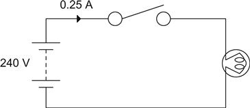
The circuit shown in Figure 1.1 is switched on, and a current of 0.25 A flows. What is the resistance of the lamp?
R=VI=2400.25=960Ω
Now this might seem like a trivial example, since we could easily have measured the resistance of the lamp to 3½ significant figures using our shiny, new, digital multimeter. But could we? The hot resistance of an incandescent lamp is very different from its cold resistance; in the example above, the cold resistance was 80 Ω.
We could now work the other way and ask how much current would flow through an 80 Ω resistor connected to 240 V.
I=VR=24080=3A
Incidentally, this is why incandescent lamps are most likely to fail at switch-on. The high initial current that flows before the filament has warmed up and increased its resistance stresses the weakest parts of the filament, they become so hot that they vaporise, and the lamp blows.
Power
In the previous example, we looked at an incandescent lamp and rated it by the current that flowed through it when connected to a 240 V battery. But we all know that lamps are rated in watts, so there must be some connection between the two.
One watt (W) of power is expended if one joule of work is done in one second.
power(watts)=workdone(joules)timetaken(seconds)P=Wt
This may not seem to be the most useful of definitions, and, indeed, it is not, but by combining it with some earlier equations:
W=QV
So:
P=QVt
But:
Q=It
So:
P=IVtt
We obtain:
This is a fundamental equation of equal importance to Ohm’s law. Substituting the Ohm’s law equations into this yields:

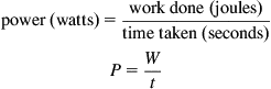
We can now use these equations to calculate the power rating of our lamp. Since it drew 0.25 A when fed from 240 V, and had a hot resistance of 960 Ω, we can use any of the three equations.
Using:
P=V2RP=2402960P=60W
It will probably not have escaped your notice that this lamp looks suspiciously like an AC mains lamp, and that the battery was rather large. We will return to this later.
Kirchhoff’s Laws
There are two of these: a current law and a voltage law. They are both very simple and, at the same time, very powerful.
The current law states:
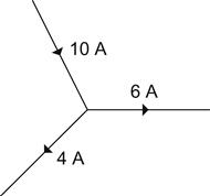
The algebraic sum of the currents flowing into, and out of, a node is equal to zero.
0=I1+I2+I3+⋯
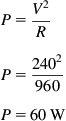
What it says in a more relaxed form is that what goes in, comes out. If we have 10 A going into a node, or junction, then that much current must also leave that junction – it might not all come out on one wire, but it must all come out. A conservation of current, if you like (see Figure 1.2).
currentflowingintothenode:I1=10Acurrentsleavingthenode:I2=4AI3=6Atotalcurrentleavingthenode:Itotal=10A
From the point of view of the node, the currents leaving the node are flowing in the opposite direction to the current flowing into the node, so we must give them a minus sign before plugging them into the equation.
0=I1+I2+I3=10A+(−4A)+(−6A)=10−4−6
This may have seemed pedantic, since it was obvious from the diagram that the incoming currents equalled the outgoing currents, but you may need to find a current when you do not even know the direction in which it is flowing. Using this convention forces the correct answer!
It is vital to make sure that your signs are correct.
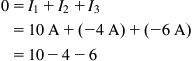
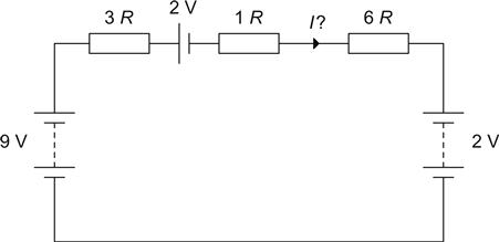
The voltage law states:
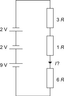
This law draws a very definite distinction between EMFs and potential differences. EMFs are the sources of electrical energy (such as batteries), whereas potential differences are the voltages dropped across components. Another way of stating the law is to say that the algebraic sum of the EMFs must equal the algebraic sum of the potential drops around the loop. Again, you could consider this to be a conservation of voltage (see Figure 1.3).
Resistors in Series and Parallel
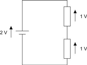
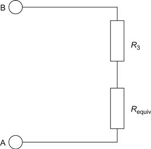
If we had a network of resistors, we might want to know what the total resistance was between terminals A and B (see Figure 1.4).
We have three resistors: R1 is in parallel with R2, and this combination is in series with R3.
As with all problems, the thing to do is to break it down into its simplest parts. If we had some means of determining the value of resistors in series, we could use it to calculate the value of R3 in series with the combination of R1 and R2, but as we do not yet know the value of the parallel combination, we must find this first. This question of order is most important, and we will return to it later.
If the two resistors (or any other component, for that matter) are in parallel, then they must have the same voltage drop across them. Ohm’s law might therefore, be a useful starting point.
I=VR
Using Kirchhoff’s current law, we can state that:
Itotal=IR1+IR2+⋯
So:
VR=VR1+VR2+⋯
Dividing by V:
1R=1R1+1R2+⋯
The reciprocal of the total parallel resistance is equal to the sum of the reciprocals of the individual resistors.
For the special case of only two resistors, we can derive the equation:
This is often known as ‘product over sum’, and whilst it is useful for mental arithmetic, it is slow to use on a calculator (more keystrokes).
Now that we have cracked the parallel problem, we need to crack the series problem.
First, we will simplify the circuit. We can now calculate the total resistance of the parallel combination and replace it with one resistor of that value – an equivalent resistor (see Figure 1.5).
Using the voltage law, the sum of the potentials across the resistors must be equal to the driving EMF:
Vtotal=VR1+VR2+⋯
Using Ohm’s law:
Vtotal=IR1+IR2+⋯
But if we are trying to create an equivalent resistor, whose value is equal to the combination, we could say:
IRtotal=IR1+IR2+⋯
Hence:
Rseries=R1+R2+⋯
Using the parallel and series equations, we are now able to calculate the total resistance of any network (see Figure 1.6).
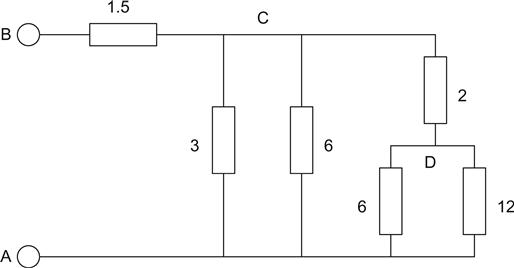
Now this may look horrendous, but it is not a problem if we attack it logically. The hardest part of the problem is not wielding the equations or numbers, but where to start.
We want to know the resistance looking into the terminals A and B, but we do not have any rules for finding this directly, so we must look for a point where we can apply our rules. We can apply only one rule at a time, so we look for a combination of components made up only of series or parallel components.
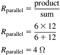
In this example, we find that between node A and node D there are only parallel components. We can calculate the value of an equivalent resistor and substitute it back into the circuit:
Rparallel=productsumRparallel=6×126+12Rparallel=4Ω
We redraw the circuit (see Figure 1.7).
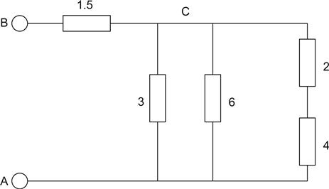
Looking again, we find that now the only combinations made up of series or parallel components are between node A and node C, but we have a choice – either the series combination of the 2 Ω and 4 Ω, or the parallel combination of the 3 Ω and 6 Ω. The one to go for is the series combination. This is because it will result in a single resistor that will then be in parallel with the 3 Ω and 6 Ω resistors. We can cope with the three parallel resistors later:
Rseries=R1+R2Rseries=4+2Rseries=6Ω
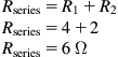
We redraw the circuit (see Figure 1.8).
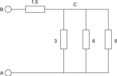
We now see that we have three resistors in parallel:
IR=IR1+IR2+IR3IR=13+16+16IR=23
Hence:
R=32=1.5Ω
We have reduced the circuit to two 1.5 Ω resistors in series, and so the total resistance is 3 Ω.
This took a little time, but it demonstrated some useful points that will enable you to analyse networks much faster the second time around:
• The critical stage is choosing the starting point.
• The starting point is generally as far away from the terminals as it is possible to be.
• The starting point is made up of a combination of only series or parallel components.
• Analysis tends to proceed outwards from the starting point towards the terminals.
• Redrawing the circuit helps. You may even need to redraw the original circuit if it does not make sense to you. Redrawing as analysis progresses reduces confusion and errors – do it!
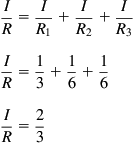
Potential Dividers
Figure 1.9 shows a potential divider. This could be made up of two discrete resistors, or it could be the moving wiper of a volume control. As before, we will suppose that a current I flows through the two resistors. We want to know the ratio of the output voltage to the input voltage (see Figure 1.9).
Vout=IR2V=IR1+IR2V=I(R1+R2)

Hence:
VoutV=IR2I(R1+R2)
This is a very important result and, used intelligently, can solve virtually anything.
Equivalent Circuits
We have looked at networks of resistors and calculated equivalent resistances. Now we will extend the idea to equivalent circuits. This is a tremendously powerful concept for circuit analysis.
It should be noted that this is not the only method, but it is usually the quickest and kills 99% of all known problems. Other methods include Kirchhoff’s laws combined with lots of simultaneous equations and the superposition theorem. These methods may be found in standard texts, but they tend to be cumbersome, so we will not discuss them here.
The Thévenin Equivalent Circuit
When we looked at the potential divider, we were able to calculate the ratio of output voltage to input voltage. If we were now to connect a battery across the input terminals, we could calculate the output voltage. Using our earlier tools, we could also calculate the total resistance looking into the output terminals. As before, we could then redraw the circuit, and the result is known as the Thévenin equivalent circuit. If two black boxes were made, one containing the original circuit and the other the Thévenin equivalent circuit, you would not be able to tell from the output terminals which was which. The concept is simple to use and can break down complex networks quickly and efficiently (see Figure 1.10).
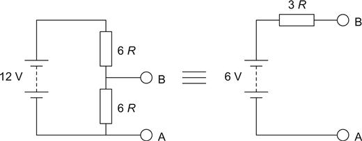
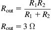
This is a simple example to demonstrate the concept. First, we find the equivalent resistance, often known as the output resistance. Now, in the world of equivalent circuits, batteries are perfect voltage sources; they have zero internal resistance and look like a short circuit when we consider their resistance. Therefore, we can ignore the battery, or replace it with a piece of wire whilst we calculate the resistance of the total circuit:
Routput=R1R2R1+R2Routput=3Ω
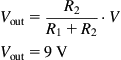
Next, we need to find the output voltage. We will use the potential divider equation:
VoutV=R2R1+R2VoutV=12
So:
Vout=12VVout=6V

Now for a much more complex example. This will use all the previous techniques and really demonstrate the power of Thévenin (see Figure 1.11).
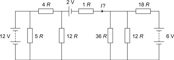
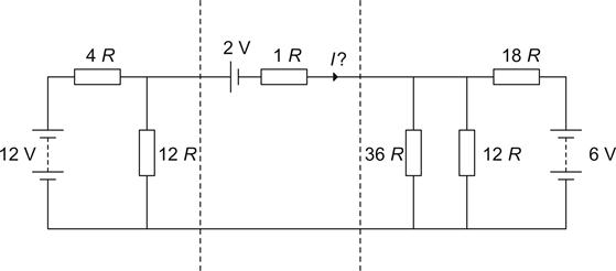
For some obscure reason, we want to know the current flowing in the 1 Ω resistor. The first thing to do is to redraw the circuit. Before we do this we can observe that the 5 Ω resistor in parallel with the 12 V battery is irrelevant. Yes, it will draw current from the battery, but it does not affect the operation of the rest of the circuit. A short circuit in parallel with 5 Ω is still a short circuit, so we will throw it away (see Figure 1.12).
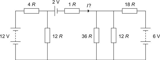
Despite our best efforts, this is still a complex circuit, so we need to break it down into modules that we recognise. Looking at the left-hand side, we find a battery with a 4 Ω and 12 Ω resistor which looks suspiciously like the simple problem that we saw earlier, so let us break the circuit there and make an equivalent circuit (see Figure 1.13).
Using the potential divider rule:
Vout=R2R1+R2·VVout=9V
Using ‘product over sum’:
Rout=R1R2R1+R2Rout=3Ω
Looking at the right-hand side, we can perform a similar operation to the right of the dashed line.
First, we find the resistance of the parallel combination of the 36 Ω and 12 Ω resistors, which is 9 Ω. We now have a potential divider, whose output resistance is 6 Ω and the Thévenin voltage is 2 V.
Now we redraw the circuit (see Figure 1.14).
We can make a few observations at this point. First, we have three batteries in series, why not combine them into one battery? There is no reason why we should not do this provided that we take note of their polarities. Similarly, we can combine some, or all, of the resistors (see Figure 1.15).
The problem now is trivial, and a simple application of Ohm’s law will solve it. We have a total resistance of 10 Ω and a 5 V battery, so the current must be 0.5 A.
• Look for components that are irrelevant, such as resistors directly across battery terminals.
• Look for potential dividers on the outputs of batteries and ‘Thévenise’ them. Keep on doing so until you meet the next battery.
• Work from battery terminals outwards.
• Keep calm, and try to work neatly – it will save mistakes later.
Although it is possible to solve most problems using a Thévenin equivalent circuit, sometimes a Norton equivalent is more convenient.
The Norton Equivalent Circuit
The Thévenin equivalent circuit was a perfect voltage source in series with a resistance, whereas the Norton equivalent circuit is a perfect current source in parallel with a resistance (see Figure 1.16).
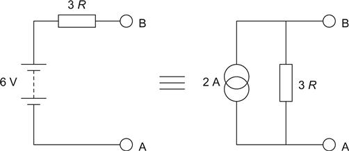
We can easily convert from a Norton source to a Thévenin source, or vice versa, because the resistor has the same value in both cases. We find the value of the current source by short circuiting the output of the Thévenin source and calculating the resulting current – this is the Norton current.
To convert from a Norton source to a Thévenin source, we leave the source open circuit and calculate the voltage developed across the Norton resistor – this is the Thévenin voltage.
For the vast majority of problems, the Thévenin equivalent will be quicker, mostly because we become used to thinking in terms of voltages that can easily be measured by a meter or viewed on an oscilloscope. Occasionally, a problem will arise that is intractable using Thévenin, and converting to a Norton equivalent causes the problem to solve itself. Norton problems usually involve the summation of a number of currents, when the only other solution would be to resort to Kirchhoff and simultaneous equations.
Units and Multipliers
All the calculations up to this point have been arranged to use convenient values of voltage, current and resistance. In the real world, we will not be so fortunate, and to avoid having to use scientific notation, which takes longer to write and is virtually unpronounceable, we will prefix our units with multipliers [1].
| Prefix | Abbreviation | Multiplies by |
| yocto | y | 10−24 |
| zepto | z | 10−21 |
| atto | a | 10−18 |
| femto | f | 10−15 |
| pico | p | 10−12 |
| nano | n | 10−9 |
| micro | μ | 10−6 |
| milli | m | 10−3 |
| kilo | k | 103 |
| mega | M | 106 |
| giga | G | 109 |
| tera | T | 1012 |
| peta | P | 1015 |
| exa | E | 1018 |
| zetta | Z | 1021 |
| yotta | Y | 1024 |
Note that the case of the prefix is important; there is a large difference between 1 mΩ and 1 MΩ. Electronics uses a very wide range of values; small-signal pentodes have anode to grid capacitances measured in fF (F=farad, the unit of capacitance), and petabyte data stores are already common. Despite this, for day-to-day electronics use, we only need to use pico to mega.
Electronics engineers commonly abbreviate further, and you will often hear a 22 pF (picofarad) capacitor referred to as 22 ‘puff’, whilst the ‘ohm’ is commonly dropped for resistors, and 470 kΩ (kiloohm) would be pronounced as ‘four-seventy-kay’.
A rather more awkward abbreviation that arose before high-resolution printers became common (early printers could not print ‘μ’), is the abbreviation of μ (micro) to m. This abbreviation persists, particularly in the US text, and you will occasionally see a 10 mF capacitor specified, although the context makes it clear that what is actually meant is 10 μF. For this reason, true 10 mF capacitors are invariably specified as 10,000 μF.
Unless an equation states otherwise, assume that it uses the base physical units, so an equation involving capacitance and time constants would expect you to express capacitance in farads and time in seconds. Thus, 75 μs=75×10−6 s, and the value of capacitance determined by an equation might be 2.2×10⁻¹⁰ F=220 pF. Very occasionally, it is handier to express an equation using real-world units such as mA or MΩ, in which case the equation or its accompanying text will always explain this break from convention.
The Decibel
The human ear spans a vast dynamic range from the near silence heard in an empty recording studio to the deafening noise of a nearby pneumatic drill. If we were to plot this range linearly on a graph, the quieter sounds would hardly be seen, whereas the difference between the noise of the drill and that of a jet engine would be given a disproportionate amount of room on the graph. What we need is a graph that gives an equal weighting to relative changes in the level of both quiet and loud sounds. By definition, this implies a logarithmic scale on the graph, but electronics engineers went one better and invented a logarithmic ratio known as the decibel (dB) that was promptly hijacked by the acoustical engineers. (The fundamental unit is the bel, but this is inconveniently large, so the decibel is more commonly used.)
The dB is not an absolute quantity. It is a ratio, and it has one formula for use with currents and voltages and another for powers:
dB=20log10(V1V2)=20log10(I1I2)=10log10(P1P2)
The reason for this is that P∝V2 or I2, and with logarithms, multiplying the logarithm by 2 is the same as squaring the original number. Using a different formula to calculate dBs when using powers ensures that the resulting dBs are equivalent, irrespective of whether they were derived from powers or voltages.
This might seem complicated when all we wanted to do was to describe the difference in two signal levels, but the dB is a very handy unit.
Useful common dB values are:
| dB | V1/V2 | P1/P2 |
| 0 | 1 | 1 |
| 3 | √2 | 2 |
| 6 | 2 | 4 |
| 20 | 10 | 100 |
Because dBs are derived from logarithms, they obey all the rules of logarithms, and adding dBs is the same as multiplying the ratios that generated them. Note that dBs can be negative, implying loss or a drop in level.
For example, if we had two cascaded amplifiers, one with a voltage gain of 0.5 and the other with a voltage gain of 10, then by multiplying the individual gains, the combined voltage gain would be 5. Alternatively, we could find the gain in dB by saying that one amplifier had −6 dB of gain whilst the other had 20 dB, and adding the gains in dB to give a total gain of 14 dB.
When designing amplifiers, we will not often use the above example, as absolute voltages are often more convenient, but we frequently need dBs to describe filter and equalisation curves.
Alternating Current (AC)
All the previous techniques have used direct current (DC), where the current is constant and flows in one direction only. Listening to DC is not very interesting, so we now need to look at alternating currents (AC).
All of the previous techniques of circuit analysis can be applied equally well to AC signals.
The Sine Wave
The sine wave is the simplest possible alternating signal, and its equation is:
v=Vpeaksin(ωt+θ)
These mathematical concepts are shown on the diagram (see Figure 1.17).
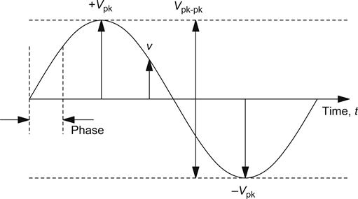
Equations involving changing quantities use a convention. Upper case letters denote DC, or constant values, whereas lower case letters denote the instantaneous AC, or changing, value. It is a form of shorthand to avoid having to specify separately that a quantity is AC or DC. It would be nice to say that this convention is rigidly applied, but it is often neglected, and the context of the symbols usually makes it clear whether the quantity is AC or DC.
In electronics, the word ‘peak’ (pk) has a very precise meaning and, when used to describe an AC waveform, it means the voltage from zero volts to the peak voltage reached, either positive or negative. Peak to peak (pk–pk) means the voltage from positive peak to negative peak, and for a symmetrical waveform, Vpk–pk=2 Vpk.
Although electronics engineers habitually use ω to describe frequency, they do so only because calculus requires that they work in radians. Since ω=2πf, we can rewrite the equation as:
v=Vpeaksin(2πft+θ)
If we now inspect this equation, we see that apart from time t, we could vary other constants before we allow time to change and determine the waveform. We can change Vpeak, and this will change the amplitude of the sine wave, or we can change f, and this will change the frequency. The inverse of frequency is period, which is the time taken for one full cycle of the waveform to occur:
period(T)=1f
If we listen to a sound that is a sine wave, and change the amplitude, this will make the sound louder or softer, whereas varying frequency changes the pitch. If we vary θ (phase), it will sound the same if we are listening to it, and unless we have an external reference, the sine wave will look exactly the same viewed on an oscilloscope. Phase becomes significant if we compare one sine wave with another sine wave of the same frequency or a harmonic of that frequency. Attempting to compare phase between waveforms of unrelated frequencies is meaningless.
Now that we have described sine waves, we can look at them as they would appear on the screen of an oscilloscope. See Figure 1.18.
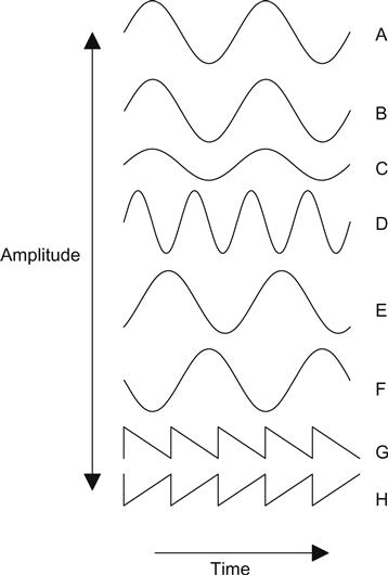
Sine waves A and B are identical in amplitude, frequency and phase. Sine wave C has lower amplitude, but frequency and phase are the same. Sine wave D has the same amplitude, but double the frequency. Sine wave E has identical amplitude and frequency to A and B, but the phase θ has been changed.
Sine wave F has had its polarity inverted. Although, for a sine wave, we cannot see the difference between a 180° phase change and a polarity inversion, for asymmetric waveforms there is a distinct difference. We should, therefore, be very careful if we say that two waveforms are 180° out of phase with each other that we do not actually mean that one is inverted with respect to the other.
The sawtooth waveform G has been inverted to produce the waveform H, and it can be seen that this is completely different from a 180° phase change. (Strictly, the UK term ‘phase splitter’ is entirely incorrect for this reason, and the US description ‘phase inverter’ is much better, but falls short of the technically correct description ‘polarity inverter’ used by nobody.)
The Transformer
When the electric light was introduced as an alternative to the gas mantle, there was a great debate as to whether the distribution system should be AC or DC. The outcome was settled by the enormous advantage of the transformer, which could step up, or step down, the voltage of an AC supply. The DC supply could not be manipulated in this way, and evolution took its course.
A transformer is essentially a pair of electrically insulated windings that are magnetically coupled to each other, usually on an iron core. They vary from the size of a fingernail to that of a large house, depending on power rating and operating frequency, with high frequency transformers being smaller. The symbol for a transformer is modified depending on the core material. Solid lines indicate a laminated iron core and dotted lines denote a dust core, whilst an air core has no lines (see Figure 1.19).

The perfect transformer changes one AC voltage to another, more convenient voltage with no losses whatsoever; all of the power at the input is transferred to the output:
P=Pout
Having made this statement, we can now derive some useful equations:
V·I=Vout·Iout
Rearranging:
VVout=IoutI=n
The new constant n is very important and is the ratio between the number of turns on the input winding and the number of turns on the output winding of the transformer. Habitually, when we talk about transformers, the input winding is known as the primary and the output winding is the secondary.
n(turnsratio)=numberofprimaryturnsnumberofsecondaryturns
Occasionally, an audio transformer may have a winding known as a tertiary winding, which usually refers to a winding used for feedback or monitoring, but it is more usual to refer to multiple primaries and secondaries.
When the perfect transformer steps voltage down, perhaps from 240 V to 12 V, the current ratio is stepped up, and each ampere of primary current is due to 20 A drawn from the secondary. This implies that the resistance of the load on the secondary is different from that seen looking into the primary. If we substitute Ohm’s law into the conservation of power equation:
V2primaryRprimary=V2secondaryRsecondaryRsecondaryRprimary=(VprimaryVsecondary)2=n2
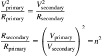
The transformer changes resistances by the square of the turns ratio. This will become very significant when we use audio transformers that must match loudspeakers to output valves.
As an example, an output transformer with a primary to secondary turns ratio of 31.6:1 would allow the output valves to see the 8 Ω loudspeaker as an 8 kΩ load, whereas the loudspeaker sees the Thévenin output resistance of the output valves stepped down by an identical amount.
The concept of looking into a device in one direction, and seeing one thing, whilst looking in the opposite direction, and seeing another, is very powerful, and we will use it frequently when we investigate simple amplifier stages.
Practical transformers are not perfect, and we will investigate their imperfections in greater detail in Chapter 4.
Capacitors, Inductors and Reactance
Previously, when we analysed circuits, they were composed purely of resistors and voltage or current sources.
We now need to introduce two new components: capacitors and inductors. Capacitors have the symbol C, and the unit of capacitance is the farad (F). 1 F is an extremely large capacitance, and more common values range from a few pF to tens of thousands of μF. Inductors have the symbol L, and the unit of inductance is the henry (H). The henry is quite a large unit, and common values range from a few μH to tens of H. Although the henry, and particularly the farad, is rather large for our very specialised use, its size derives from the fundamental requirement for a coherent system of units; a coherent system allows units (such as the farad) to be derived from base units (such as the ampere) with an absolute minimum of scaling factors.
The simplest capacitor is made of a pair of separated plates, whereas an inductor is a coil of wire, and this physical construction is reflected in their graphical symbols (see Figure 1.20).
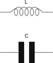
Resistors had resistance, whereas capacitors and inductors have reactance. Reactance is the AC equivalent of resistance – it is still measured in ohms and is given the symbol X. We will often have circuits where there is a combination of inductors and capacitors, so it is normal to add a subscript to denote which reactance is which:
XC=12πfCXL=2πfL

Looking at these equations, we find that reactance changes with frequency and with the value of the component. We can plot these relationships on a graph (see Figure 1.21).

An inductor has a reactance of zero at zero frequency. More intuitively, it is a short circuit at DC. As we increase frequency, its reactance rises.
A capacitor has infinite reactance at zero frequency. It is open circuit at DC. As frequency rises, reactance falls.
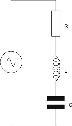
A circuit made up of only one capacitor, or one inductor, is not very interesting, and we might want to describe the behaviour of a circuit made up of resistance and reactance, such as a moving coil loudspeaker. See Figure 1.22.
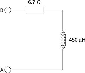
We have a combination of resistance and inductive reactance, but at the terminals A and B we see neither a pure reactance, nor a pure resistance, but a combination of the two factors known as impedance.
In a traditional electronics book, we would now lurch into the world of vectors, phasors and complex number algebra. Whilst fundamental AC theory is essential for electronics engineers who have to pass examinations, we cannot justify the mental trauma needed to cover the topic in depth, so we will simply pick out useful results that are relevant to our highly specialised field of interest.
Filters
We mentioned that reactance varies with frequency. This property can be used to make a filter that allows some frequencies to pass unchecked, whilst others are attenuated (see Figure 1.23).
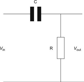
All filters are based on potential dividers. In this filter, the upper leg of the potential divider is a capacitor, whereas the lower leg is a resistor. We stated earlier that a capacitor is an open circuit at DC. This filter, therefore, has infinite attenuation at DC – it blocks DC. At infinite frequency, the capacitor is a short circuit, and the filter passes the signal with no attenuation, so the filter is known as a high-pass filter (see Figure 1.24).
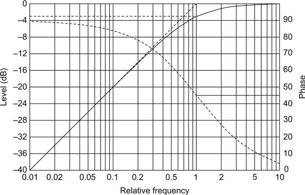
Frequency is plotted on a logarithmic scale to encompass the wide range of values without cramping. When we needed a logarithmic unit for amplitude ratios, we invented the dB, but a logarithmic unit for frequency already existed, so engineers stole the octave from the musicians. An octave is simply a halving or doubling of frequency and corresponds to eight ‘white keys’ on a piano keyboard.
The curve has three distinct regions: the stop-band, cut-off and the pass-band.
The stop-band is the region where signals are stopped or attenuated. In this filter, the attenuation is inversely proportional to frequency, and we can see that at a sufficiently low frequency (LF), the shape of the curve in this region becomes a straight line. If we were to measure the slope of this line, we would find that it tends towards 6 dB/octave.
Note that the phase of the output signal changes with frequency, with a maximum change of 90° when the curve finally reaches 6 dB/octave.
This slope is very significant, and all filters with only one reactive element have an ultimate slope of 6 dB/octave. As we add more reactive elements, we can achieve a higher slope, so filters are often referred to by their order, which is the number of reactive elements contributing to the slope. A third-order filter would have three reactive elements, and its ultimate slope would, therefore, be 18 dB/octave.
Although the curve reaches an ultimate slope, the behaviour at cut-off is of interest, not least because it allows us to say at what frequency the filter begins to take effect. On the diagram, a line was drawn to determine the ultimate slope. If this is extended until it intersects with a similar line drawn continued from the pass-band attenuation, the point of intersection is the filter cut-off frequency. (You will occasionally see idealised filter responses drawn in this way, but this does not imply that the filter response actually changes abruptly from pass-band to stop-band.)
If we now drop a line down to the frequency axis from the cut-off point, it passes through the curve, and the filter response at this point is 3 dB down on the pass-band value. The cut-off frequency is, therefore, also known as f−3 dB, or the −3 dB point, and at this point the phase curve is at its steepest, with a phase change of 45°.
Second-order filters, and above, have considerable freedom in the way that the transition from pass-band to stop-band is made, and so the class of filter is often mentioned in conjunction with names like Bessel, Butterworth and Chebychev, in honour of their originators.
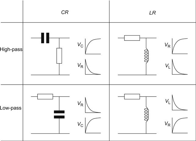
Although we initially investigated a high-pass Capacitor-Resistance (CR) filter, other combinations can be made using one reactive component and a resistor (see Figure 1.25).
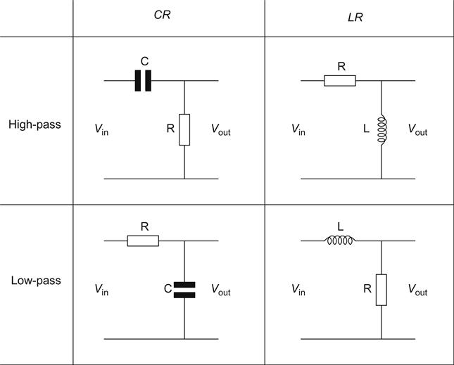
We now have a pair of high-pass filters and a pair of low-pass filters; the low-pass filters have the same slope, and cut-off frequency can be found from the graph in the same way.
Now that we are familiar with the shape of the curves of these simple filters, referring to them by their cut-off frequency and slope is more convenient (the word ‘ultimate’ is commonly neglected). For these simple filters, the equation for cut-off frequency is the same whether the filter is high-pass or low-pass. For a CR filter:
f−3dB=12πCR
And for an LR filter:
f−3dB=R2πL
Time Constants
In audio, simple filters or equalisation networks are often described in terms of their time constants. These have a very specialised meaning that we will touch upon later, but in this context they are simply used as a shorthand form of describing a first-order filter that allows component values to be calculated quickly.
For a CR network, the time constant τ (tau) is:
τ=CR
For an LR network:
τ=LR
Because it is a time constant, the unit of τ is seconds, but audio time constants are habitually given in μs. We can easily calculate the cut-off frequency of the filter from its time constant τ:
f=12πτ
Note that τ is quite distinct from period, which is given the symbol T.
Examples of audio time constants:
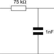
• FM analogue broadcast High Frequency de-emphasis: UK 50 μs and USA 75 μs
• RIAA vinyl record characteristic: 3,180 μs, 318 μs and 75 μs.
A 75 μs High Frequency de-emphasis circuit needs a low-pass filter, usually CR, so a pair of component values whose product equals 75 μs, 1 nF and 75 kΩ would do nicely (see Figure 1.26).
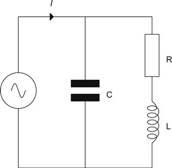
Resonance
So far, we have made filters using only one reactive component, but if we make a network using a capacitor and an inductor, we find that we have a resonant circuit. Resonance occurs everywhere in the natural world, from the sound of a tuning fork to the bucking and twisting of the Tacoma Narrows bridge. (A bridge that finally collapsed during a storm on 7 November 1940 because the wind excited a structural resonance.) A resonant electronic circuit is shown in Figure 1.27.
If we were to sweep the frequency of the source, whilst measuring the current drawn, we would find that at the resonant frequency, the current would rise to a maximum determined purely by the resistance of the resistor. The circuit would appear as if the reactive components were not there. We could then plot a graph of current against frequency (see Figure 1.28).
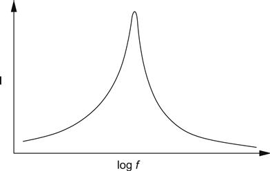
The sharpness and the height of this peak are determined by the Q or magnification factor of the circuit:
Q=1R√LC
This shows us that a small resistance can cause a high Q, and this will be very significant later. The frequency of resonance is:
f=12π√LC
Our first resonant circuit was a series resonant circuit, but parallel resonance, where the total current falls to a minimum at resonance, is also possible (see Figure 1.29).
If Q>5, the above equations are reasonably accurate for parallel resonance. We will not fret about the accuracy of resonant calculations, since we rarely want resonances in audio, and so do our best to remove or damp them.
RMS and Power
We mentioned power earlier, when we investigated the flow of current through a lamp using a 240 V battery. Mains electricity is AC and has recently been respecified in the UK to be 230 VAC +10%−6% at 50±1 Hz, but how do we define that 230 V?
If we had a valve heater filament, it would be most useful if it could operate equally well from AC or DC. As far as the valve is concerned, AC electricity will heat the filament equally well, just so long as we apply the correct voltage.
RMS is short for Root of the Mean of the Squares, which refers to the method of calculating the value. Fortunately, the ratios of VRMS to Vpeak have been calculated for the common waveforms, and in audio design we are mostly concerned with the sine wave, for which:
Vpeak=√2·VRMS
All sinusoidal AC voltages are given in VRMS unless specified otherwise, so a heater designed to operate on 6.3 VAC would work equally well connected to 6.3 VDC.
We have only mentioned RMS voltages, but we can equally well have RMS currents, in which case:
P=VRMS·IRMS
The Square Wave
Until now, all of our dealings have been with sine waves, which are pure tones. When we listen to music, we do not hear pure tones, instead we hear a fundamental with various proportions of harmonics whose frequencies are arithmetically related to the frequency of the fundamental. We are able to distinguish between one instrument and another because of the differing proportions of the harmonics and the transient at the beginning of each note.
A useful waveform for testing amplifiers quickly would have many harmonics and a transient component. The square wave has precisely these properties because it is composed of a fundamental frequency plus odd harmonics whose amplitudes steadily decrease with frequency (see Figure 1.30).
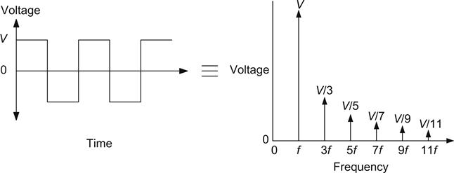
A square wave is thus an infinite series of harmonics, all of which must be summed from the fundamental to the infinite harmonic. We can express this argument mathematically as a Fourier series, where f is the fundamental frequency:
squarewave=4π∑∞n=1sin[(2n−1)·2πft]2n−1
This is a shorthand formula, but understanding the distribution of harmonics is much easier if we express them in the following form:
squarewave∝1(f)+13(3f)+15(5f)+17(7f)+19(9f)+…
We can now see that the harmonics die away very gradually and that a 1 kHz square wave has significant harmonics well beyond 20 kHz. What is not explicitly stated by these formulae is that the relative phase of these components is critical. The square wave thus tests not only amplitude response, but also phase response.
Square Waves and Transients
We briefly mentioned earlier that the square wave contained a transient component. One way of viewing a square wave is to treat it as a DC level whose polarity is inverted at regular intervals. At the instant of inversion, the voltage has to change instantaneously from its negative level to its positive level, or vice versa. The abrupt change at the leading edge of the square wave is the transient, and because it occurs so quickly, it must contain a high proportion of high frequency components. Although we already knew that the square wave contained these high frequencies, it is only at the leading edge that they all sum constructively, so any change in high frequency response is seen at this leading edge.
We have considered the square wave in terms of frequency; now we will consider it as a series of transients in time, and investigate its effect on the behaviour of CR and LR networks.
The best way of understanding this topic is with a mixture of intuitive reasoning coupled to a few graphs. Equations are available, but we very rarely need to use them.
In electronics, a step is an instantaneous change in a quantity such as current or voltage, so it is a very useful theoretical concept for exploring the response of circuits to transients. We will start by looking at the voltage across a capacitor when a voltage step is applied via a series resistor (see Figure 1.31).
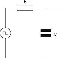
The capacitor is initially discharged (VC=0). The step is applied and switches from 0 V to +V, an instantaneous change of voltage composed mostly of high frequencies. The capacitor has a reactance that is inversely proportional to frequency and, therefore, appears as a short circuit to these high frequencies. If it is a short circuit, we cannot develop a voltage across it. The resistor, therefore, has the full applied voltage across it and passes a current determined by Ohm’s law. This current then flows through the capacitor and starts charging it. As the capacitor charges, its voltage rises, until eventually it is fully charged, and no more current flows. If no more current flows into the capacitor (IC=0), then IR=0, and so VR=0. We can plot this argument as a pair of graphs showing capacitor and resistor voltage (see Figure 1.32).
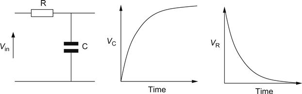
The first point to note about these two graphs is that the shape of the curve is an exponential (this term will be explained further later). The second point is that when we apply a step to a CR circuit (and even an LR circuit), the current or voltage curve will always be one of these curves. Knowing that the curve can only be one of these two possibilities, all we need to be able to do is to choose the appropriate curve.
The transient edge can be considered to be of infinitely High Frequency, and the capacitor is, therefore, a short circuit. Developing a voltage across a short circuit requires infinite current.
An inductor is the dual or inverse of a capacitor, and so an inductor has a similar rule.
We can now draw graphs for each of the four combinations of CR and LR circuits when the same step in voltage is applied (see Figure 1.33).
Having stated that the shape of the curves in each of the four cases is identical, we can now examine the fundamental curves in a little more detail.
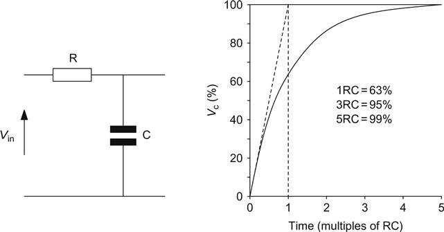
Using the original CR circuit as an example, the capacitor will eventually charge to the input voltage, so we can draw a dashed line to represent this voltage. The voltage across the capacitor has an initial slope, and if we continue this slope with another dashed line, we will find that it intersects the first line at a time that corresponds to CR, which is the time constant that we met earlier. The CR time constant is defined as the time taken for the capacitor voltage to reach its final value had the initial rate of charge been maintained (see Figure 1.34).
The equation for the falling curve is:
v=V·et/τ
The equation for the rising curve is:
v=V·(1−et/τ)
where ‘e’ is the base of natural logarithms and is the key marked ‘ex’ or ‘exp’ on your scientific calculator. These curves derive their names because they are based on an exponential function.
We could now find what voltage the capacitor actually achieved at various times. Using the equation for the rising curve:
| 1τ | 63% |
| 3τ | 95% |
| 5τ | 99% |
Because the curves are all the same shape, these ratios apply to all four of the CR and LR combinations. The best way to use the ratios is to first decide which way the curve is heading; the ratios then determine how much of the change will be achieved, and in what time.
Note that after 5τ, the circuit has very nearly reached its final position or steady state. This is a useful point to remember when considering what will happen at switch-on to high voltage semiconductor circuits.
When we considered the response to a single step, the circuit eventually achieved a steady state because there was sufficient time for the capacitor to charge or for the inductor to change its magnetic field. With a square wave, this may no longer be true. As was mentioned before, the square wave is an excellent waveform for testing audio amplifiers, not least because oscillators that can generate both sine and square waves are fairly cheaply available.
If we apply a square wave to an amplifier, we are effectively testing a CR circuit made up of a series resistance and a capacitance to ground (often known as a shunt capacitance). We should, therefore, expect to see some rounding of the leading edges, because some of the high frequencies are being attenuated.
If the amplifier is only marginally stable (because it contains an unwanted resonant circuit), the high frequencies at the leading edges of the square wave will excite the resonance, and we may see a damped train of oscillations following each transition.
We can also test low frequency response with a square wave. If the coupling capacitors between stages are small enough to change their charge noticeably within one half-cycle of the square wave, then we will see tilt on the top of the square wave. Downward tilt, more commonly called sag, indicates low frequency loss, whilst upward tilt indicates low frequency boost. This is a very sensitive test of low frequency response, and if it is known that the circuit being measured includes a single high-pass filter, but with a cut-off frequency too low to be measured directly with sine waves, then a square wave may be used to infer the sine wave f−3 dB point. The full derivation of the equation that produced the following table is given in the Appendix, but if we apply a square wave of frequency f (Table 1.1).
Table 1.1
Relating Square Wave Sag to Low Frequency Cut-Off Frequency
| Sag observed using a square wave of frequency f (%) | Ratio of applied square wave frequency (f) to low frequency cut-off (f−3 dB) |
| 10 | 30 |
| 5 | 60 |
| 1 | 300 |
Most analogue audio oscillators are based on the Wien bridge and, because of amplitude stabilisation problems, rarely produce frequencies lower than ≈10 Hz. 10% and 5% square wave sag may be measured relatively easily on an oscilloscope and can, therefore, be used to infer sine wave performance at frequencies below 10 Hz.
Another useful test is to apply a high-level, High Frequency sine wave. If at all levels and frequencies, the output is still a sine wave, then the amplifier is likely to be free of slewing distortion. If the output begins to look like a triangular waveform, this is because one, or more, of the stages within the amplifier is unable to fully charge or and discharge a shunt capacitance sufficiently quickly. The distortion is known as slewing distortion because the waveform is unable to slew correctly from one voltage to another. The solution is usually to increase the anode current of the offending stage, thereby enabling it to charge or discharge the capacitance.
Random Noise
The signals that we have previously considered have been repetitive signals – we could always predict precisely what the voltage level would be at any given time. Besides these coherent signals, we shall now consider noise.
Noise is all around us, from the sound of waves breaking on a seashore, and the radio noise of stars, to the daily fluctuations of the stock markets. Electrical noise can generally be split into one of two categories: white noise, which has constant level with frequency (like white light), and 1/f noise, whose amplitude is inversely proportional to frequency.
White noise is often known as Johnson or thermal noise and is caused by the random thermal movement of atoms knocking the free electrons within a conductor. Because it is generated by a thermal mechanism, cooling critical devices reduces noise, so the input transistor associated with a High Purity Germanium (HPGe) detector used for gamma radiation spectroscopy is also cooled by the liquid nitrogen (77 K) needed to reduce leakage currents in the crystal, but some radio telescopes need the much colder liquid helium (4 K) for their head amplifiers. All resistors produce white noise and generate a noise voltage:
vnoise=√4kTBR
k=Boltzmann’s constant ≈1.381×10⁻²³ J/K
T=absolute temperature of the conductor šC+273.16
From this equation, we can see that if we were to cool the conductor to 0 K or −273.16 °C, there would be no noise because this would be absolute zero, at which temperature there is no thermal vibration of the atoms to produce noise.
The bandwidth of the measuring system is important too because the noise is proportional to the square root of bandwidth. Bandwidth is the difference between the upper and the lower f−3 dB limits of measurement. It is important to realise that in audio work, the noise measurement bandwidth is always that of the human ear (20 Hz to 20 kHz), and although one amplifier might have a wider bandwidth than another, this does not necessarily mean that it will produce any more noise.
In audio, we cannot alter the noise bandwidth or the value of Boltzmann’s constant and reducing the temperature is expensive, so our main weapon for reducing noise is to reduce resistance. We will look into this in more detail in Chapters 3 and 7.
1/f noise is also known as flicker noise or excess noise, and it is a particularly insidious form of noise because it is not predictable. It could almost be called ‘imperfection’ noise because it is generally caused by imperfections such as imperfectly ‘clean rooms’ used for making semiconductors or valves, ‘dry’ soldered joints, poor metal-to-metal contacts in connectors – the list is endless. Semiconductor manufacturers usually specify the 1/f noise corner, where the 1/f noise becomes dominant over white noise, for their devices, but equivalent data do not exist for valves.
Because noise is random, or uncorrelated, we cannot add noise voltages or currents, but must add noise powers, and some initially surprising results emerge. Noise can be considered statistically as a deviation from a mean value. When an opinion poll organisation uses as large a sample as possible to reduce error, it is actually averaging the noise to find the mean value.
If we parallel n input devices in a low-noise amplifier, the uncorrelated noise sources begin to cancel, but the wanted signal remains at constant level, resulting in an improvement in signal to noise ratio of √n dB. This technique is feasible for semiconductors where it is possible to make 100 matched parallelled transistors on a single chip (LM394, MAT-01, etc.), but we are lucky to find a pair of matched triodes in one envelope, let alone more than that!
Active Devices
We have investigated resistors, capacitors, inductors and transformers, but these were all passive components. We will now look at active devices, which can amplify a signal. All active devices need a power supply because amplification is achieved by the source controlling the flow of energy from a power supply into a load via the active device.
We will conclude this chapter by looking briefly at semiconductors. It might seem odd that we should pay any attention at all to semiconductors, but a modern valve amplifier generally contains rather more semiconductors than valves, so we need some knowledge of these devices to assist the design of the (valve) amplifier.
Conventional Current Flow and Electron Flow
When electricity was first investigated, the electron had not been discovered, and so an arbitrary direction for the flow of electricity was assumed. There was a 50/50 chance of guessing correctly, and the early researchers were unlucky. By the time the mistake was discovered and it was realised that electrons flowed in the opposite direction to the way that electricity had been thought to flow, it was too late to change the convention.
We are, therefore, saddled with a conventional current that flows in the opposite direction to that of the electrons. Mostly, this is of little consequence, but when we consider the internal workings of the transistor and the valve, we must bear this distinction in mind.
Silicon Diodes
Semiconductor devices are made by doping regions of crystalline silicon to form areas known as N-type or P-type. These regions are permanently charged and at their junction this charge forms a potential barrier that must be overcome before forward conduction can occur. Reverse polarity strengthens the potential barrier, so no conduction occurs.
The diode is a device that allows current to flow in one direction, but not the other. Its most basic use is, therefore, to rectify AC into DC. The arrow-head on the diode denotes the direction of conventional current flow, and RL is the load resistance (see Figure 1.35).
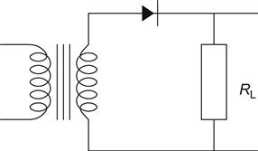
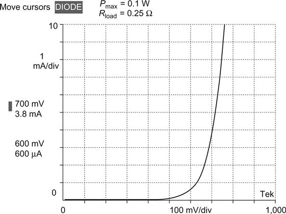
Practical silicon diodes are not perfect rectifiers and require a forward bias voltage before they conduct any appreciable current. At room temperature, this bias voltage is between 0.6 V and 0.7 V (see Figure 1.36).
This forward bias voltage is always present, so the output voltage is always less than the input voltage by the amount of the diode drop. Because there is always a voltage drop across the diode, current flow must create heat, and sufficient heat will melt the silicon. All diodes, therefore, have a maximum current rating.
In addition, if the reverse voltage is too high, the diode will break down and conduct; if this reverse current is not limited, the diode will be destroyed.
Unlike valves, the mechanism for conduction through the most common (bipolar junction) type of silicon diode is complex and results in a charge being temporarily stored within the diode. When the diode is switched off by the external voltage, the charge within the diode is quickly discharged and produces a brief current overshoot that can excite external resonances. Fortunately, Schottky diodes do not exhibit this phenomenon, and soft recovery types are fabricated to minimise it.
Voltage References
The forward voltage drop across a diode junction is determined by the Ebers/Moll equation involving absolute temperature and current, whilst the reverse breakdown voltage is determined by the physical construction of the individual diode. This means that we can use the diode as a rectifier or as a voltage reference.
Voltage references are also characterised by their slope resistance, which is the Thévenin resistance of the voltage reference when operated correctly. It does not imply that large currents can be drawn, merely that for small current changes in the linear region of operation, the voltage change will be correspondingly small.
Voltage references based on the forward voltage drop are known as bandgap devices, whilst references based on the reverse breakdown voltage are known as Zener diodes. All voltage references should pass only a limited current to avoid destruction, and ideally a constant current should be passed.
Zener diodes are commonly available in power ratings up to 75 W, although the most common rating is 400 mW, and voltage ratings are from 2.7 V to 270 V. In reality, true Zener action occurs at ≤5 V, so a ‘Zener’ diode with a rating ≥5 V actually uses the avalanche effect [2]. This is fortuitous because producing a 6.2 V device requires both effects to be used in proportions that cause the two different mechanisms to cancel the temperature coefficient almost to zero and reduce slope resistance. Diodes such as the 1N82* series deliberately exploit this phenomenon to produce a 6.2 V reference with vanishingly low temperature coefficient (0.0005%/°C for the 1N829A), but note that this performance only obtains if a Zener current of 7.5 ± 0.01 mA is used. Slope resistance rises sharply below 6 V, and more gradually above 6 V, but is typically ≈10 Ω at 5 mA for a 6.2 V Zener.
Bandgap references are often actually a complex integrated circuit and usually have an output voltage of 1.2 V, but internal amplifiers may increase this to 10 V or more. Because they are complex internally, bandgap references tend to be more expensive than Zeners, and we may occasionally need a cheap low-noise reference. Light Emitting Diodes (LEDs) and small-signal diodes are operated forward biassed, so they are quiet and reasonably cheap (Table 1.2).
Table 1.2
Comparison of Forward Drops and Slope Resistances for Various Diodes
| Diode type | Typical forward drop at 10 mA (V) | Typical rslope at 10 mA (Ω) |
| Small-signal silicon diode (1N4148) | 0.75 | 6.0 |
| Infrared LED (950 nm) | 1.2 | 5.4 |
| Cheap red LED | 1.7 | 4.3 |
| Cheap yellow, yellow/green LED | ≈2 | 10 |
| True green LED (525 nm) | 3.6 | 30 |
| Blue LED (426 nm) | 3.7 | 26 |
The Agilent HLMP6000 red LED is particularly useful as a low-noise voltage reference (see Figure 1.37).
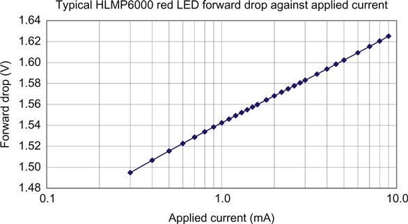
A straight line on a logarithmic scale implies a logarithmic equation:
V=0.0378lnIDC(mA)+1.5418
More significantly, differentiating the equation gives us dV/dI, which we know as slope resistance:
rslope(Ω)=37.8IDC(mA)
Thus, a typical HLMP6000 passing 10 mA has a slope resistance of 3.8 Ω. Note that this is an example of an equation where it was more useful to use the scaled unit (mA) than the base unit (A).
Bandgap references usually incorporate an internal amplifier, so their output resistance is much lower, typically stated as ≈0.2 Ω or less, but this rises with frequency. So if low resistance must be maintained to high frequencies (>1 MHz), the HLMP6000 may be a better choice.
Bipolar Junction Transistors (BJTs)
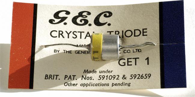
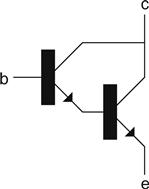
BJTs are the most common type of transistor; they are available in NPN and PNP types and can be used to amplify a signal. The name transistor is derived from transferred resistor. Before the appellation ‘transistor’ became commonplace, they were rather charmingly known as crystal triodes (see Figure 1.38).
We can imagine an NPN transistor as a sandwich of two thick slabs of N-type material separated by an extremely thin layer of P-type material. The P-type material is the base, whilst one of the N-types is the emitter and emits electrons, which are then collected by the other N-type, which is known as the collector.
If we simply connect the collector to the positive terminal of a battery and the emitter to the negative, no current will flow because the negatively charged base repels electrons. If we now apply a positive voltage to the base to neutralise this charge, the electrons will no longer be repelled, but because the base is so thin, the attraction of the strongly positively charged collector pulls most of the electrons straight through the base to the collector, and collector current flows.
The base/emitter junction is now a forward biassed diode, so it should come as no surprise to learn that 0.7 V is required across the base/emitter junction to cause the transistor to conduct electrons from emitter to collector. Because the base is so thin and the attraction of the collector is so great, very few electrons emerge from the base as base current, so the ratio of collector current to base leakage current is high. The transistor, therefore, has current gain, which is sometimes known as β (beta) but more commonly as hFE for DC current gain or hfe for AC current gain, although for all practical purposes, hFE=hfe, making the AC distinction trivial. (hFE: hybrid model, forward current transfer ratio and emitter as common terminal. Don’t you wish you hadn’t asked?)
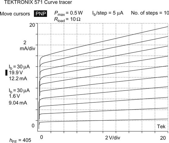
Realistically, hFE is a defect, not a parameter, and should be treated as such. It is not constant between samples and varies as device parameters change (see Figure 1.39).
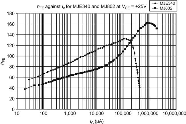
As can be seen, there is a general trend for hFE to rise with increasing collector current but fall sharply as IC(max) is approached. The MJ802 is a special audio power transistor that has been engineered to maintain hFE at high currents, and this accounts for the kink at 40 mA.
A far more important and predictable parameter is the transconductance (more usefully called mutual conductance in valves) gm, which is the change in collector current caused by a change in base/emitter voltage:
gm=ΔLCΔVBE
When we look at valves, we will see that we must always measure gm at the operating point, perhaps from a graph. For transistors, transconductance is defined by the Ebers/Moll [3] equation, and for small currents (less than ≈100 mA), gm can be estimated for any BJT using:
gm≈35IC
The Common Emitter Amplifier
Now that we have a means of predicting the change in collector current caused by a change in VBE, we could connect a resistor RL in series with the collector and the supply to convert the current change into a voltage change. By Ohm’s law:
ΔVCE=ΔIC·RL
But ΔIC=gm·ΔVBE, so:
ΔVCE=ΔVBE·gm·RLΔVCEΔVBE=Av=gm·RL
We are now able to find the voltage amplification Av (also known as gain) for this circuit, which is known as a common emitter amplifier because the emitter is common to both the input and the output circuits or ports. Note that the output polarity of the amplifier is inverted with respect to the input signal (see Figure 1.40).
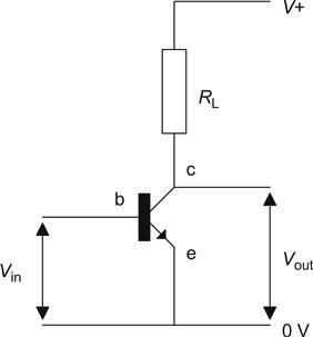
As the circuit stands, it is not very useful because any input voltage below +0.7 V will not be amplified, so the amplifier creates considerable distortion.
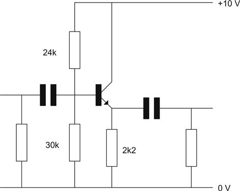
To circumvent this, we assume that the collector voltage is set to half the supply voltage because this allows the collector to swing an equal voltage both positively and negatively. Because we know the voltage across the collector load RL and its resistance, we can use Ohm’s law to determine the current through it – which is the same as the transistor collector current. We could then use the relationship between IB and IC to set this optimum collector current. As we saw earlier, the value of hFE for a transistor is not guaranteed and varies widely between devices. For a small-signal transistor, it could range from 50 to more than 400. The way around this is to add a resistor in the emitter and to set a base voltage (see Figure 1.41).
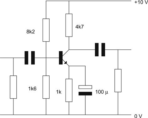
The amplifier now has input and output coupling capacitors and an emitter decoupling capacitor. The entire circuit is known as a stabilised common emitter amplifier and is the basis of most linear transistor circuitry.
Considering DC Conditions
The potential divider chain passes a current that is at least 10 times the expected base current and therefore sets a fixed voltage at the base of the transistor independent of base current. Because of diode drop, the voltage at the emitter is thus 0.7 V lower. The emitter resistor has a fixed voltage across it, and it must, therefore, pass a fixed current from the emitter. IE=IC−IB, but since IB is so small, IE≈IC, and if we have a fixed emitter current, then collector current is also fixed.
The emitter is decoupled to prevent negative feedback from reducing the AC gain of the circuit. We will consider negative feedback later in this chapter.
Briefly, if the emitter resistor was not decoupled, then any change in collector current (which is the same as emitter current) would cause the voltage across the emitter resistor to change with the applied AC. The emitter voltage would change, and vbe would effectively be reduced, causing AC gain to fall. The decoupling capacitor is a short circuit to AC and, therefore, prevents this reduction of gain. This principle will be repeated in the next chapter when we look at the cathode bypass capacitor in a valve circuit.
Input and Output Resistances
In a valve amplifier, we will frequently use transistors as part of a bias network or as part of a power supply, and being able to determine input and output resistances is, therefore, important. The following AC resistances looking into the transistor do not take account of any external parallel resistance from the viewed terminal to ground.
The output resistance 1/hoe looking into the collector is high, typically tens of kΩ at IC≈1 mA, which suggests that the transistor would make a good constant current source (hoe: hybrid model, output admittance and emitter as common terminal). In theory, if all the collector curves of a bipolar junction transistor are extended negatively, they intersect at a voltage known as the Early [4] voltage. Sadly, the real world is not so tidy, and attempts by the author to determine Early voltages resembled the result of dropping a handful of uncooked spaghetti on the graph paper. Nevertheless, the concept of Early effect is useful because it indicates that 1/hoe falls as IC rises (see Figure 1.42).
The Early effect is caused by the depletion region straddling the reverse-biassed base/collector junction. As VCB rises, the depletion region widens, effectively making the base narrower and less able to capture electrons; this increases hfe and results in increased collector current at higher collector voltages.
The resistance looking into the emitter is low, re=1/gm, so ≈20 Ω is typical. If the base is not driven by a source of zero resistance (Rb≠0), there is an additional series term, and re is found from:
re=1gm+Rbhfe
where Rb is the Thévenin resistance of all the paths to ground and supply seen from the base of the transistor. Note that even though we are no longer explicitly including a battery as the supply, the supply is still assumed to have zero output resistance from DC to light frequencies.
Looking into the base, the path to ground is via the base emitter junction in series with the emitter resistor. If the emitter resistor is not decoupled, then the resistance will be:
rb=hfe(1gm+Re)
If the emitter resistor is decoupled, then Re=0, and the equation reduces to:
rb=hfegm=hie
The AC input resistance owing purely to the base/emitter junction is often known as hie and is generally quite low, <10 kΩ (hie: hybrid model, input resistance and emitter as common terminal).
If we now consider the effect of the external parallel resistances, we see that the input resistance of the amplifier is low, typically <5 kΩ. The output resistance seen at the emitter is low, typically <100 Ω (even if the source resistance is quite high), and the output resistance at the collector is ≈RL.
The Emitter Follower
Very occasionally, you will see this amplifier called a common collector amplifier, although this phraseology is rare because it does not convey clearly what the circuit does.
If we reduce the collector load to zero and take our output from the emitter, then we have an amplifier with Av≈1. The voltage gain must be ≈1 because VE=VB−0.7 V; the emitter follows the base voltage, and the amplifier is non-inverting. Although Av=1, the current gain is much greater, and we can calculate input and output resistances using the equations presented for the common emitter amplifier (see Figure 1.43).
Because of its low output resistance and moderately high input resistance, the emitter follower is often used as a buffer to match high-impedance circuitry to low-resistance loads.
The Darlington Pair
Sometimes, even an emitter follower may not have sufficient current gain, and the solution is to use a Darlington pair; this is effectively two transistors in cascade, with one forming the emitter load for the other (see Figure 1.44).
The two transistors form a composite transistor with VBE=1.4 V and hFE (total)=hFE1×hFE2. A Darlington pair can replace a single transistor in any configuration if it seems useful. Common uses are in the output stage of a power amplifier and in linear power supplies. Darlingtons can be bought in a single package, but making your own out of two discrete transistors usually gives better performance and is cheaper in terms of component cost, although putting two parts instead of one on a Printed Circuit Board (PCB) is more expensive.
General Observations on BJTs
We mentioned earlier that the BJT could be considered to be a sandwich with the base separating the collector and the emitter. We can now develop this model and use it to make some useful generalisations, particularly about the defect known as hFE.
As the base becomes thicker, it becomes more and more probable that an electron passing from the emitter to the collector will be captured by the base and flow out of the base as base current; hFE is, therefore, inversely proportional to base thickness.
When a transistor passes a high collector current, its base current must be proportionately high. In order for the base not to melt due to this current, the base must be thickened. The thicker base reduces hFE, and required base current must rise yet further, requiring an even thicker base. hFE is, therefore, inversely proportional to the square of maximum permissible collector current, and high-current transistors have low hFE.
High-voltage transistors need a thick base to allow for the widened depletion region caused by a high collector to base voltage, so high-voltage transistors also have low hFE.
High-current transistors must have a large silicon die area in order for the collector not to melt – this large area increases collector/base capacitance. The significance of capacitance in amplifying devices will be made clear when we consider the Miller effect in Chapter 2, but for the moment we can simply say that high-current transistors will be slow.
We have barely scratched the surface of semiconductor devices and circuits. Other semiconductor circuits will be presented as and when they are needed.
Feedback
Feedback is a process whereby we take a fraction of the output of an amplifier and sum it with the input. If, when we sum it with the input, it causes the gain of the amplifier to increase, then it is known as positive feedback, and this is the basis of oscillators. If it causes the gain to fall, then it is known as negative feedback, and this technique is widely used in audio amplifiers.
The Feedback Equation
The description of feedback was deliberately rather vague because there are many ways that feedback can be applied, and they each have differing effects. Before we can look at these effects, we need a few definitions and a simple equation:
A=A01+βA0
This is the general feedback equation that defines how the gain of an amplifier will be modified by the application of feedback. β is the feedback fraction and is the proportion of the output that is fed, or looped, back to the input. It is because β is so commonly used in the feedback equation that the apparently clumsy term hFE is more popular for bipolar transistor current gain.
If βA0 is very large and positive (causing negative feedback – a reduction of gain), then βA0≈βA0+1, and the gain of the amplifier becomes:
A=1β
A0 no longer affects A, and the closed loop gain of the amplifier is determined solely by the network that provides the feedback signal.
This result is very significant because it implies many things:
• Distortion is produced by variations in gain from one voltage level to another. If open loop gain is no longer part of the equation, then small variations in this gain are irrelevant, and the amplifier produces no distortion.
• If the feedback acts to maintain the correct gain under all circumstances, then it must change the apparent input and output resistances of the amplifier.
• If the feedback fraction β is set by pure resistors, then the equation for closed loop gain does not contain any term including frequency. Theoretically, the output amplitude is, therefore, independent of frequency.
In the late 1970s, when cheap gain became readily available, designers became very excited by the possibilities and implications of the feedback equation, and set out to exploit it by designing amplifiers that were thought to have very high levels of feedback. In practice, these amplifiers did not have high levels of feedback at all frequencies and power levels, and it was the lack of feedback to linearise these fundamentally flawed circuits that caused their poor sound quality.
Before we explore the expected benefits of feedback, we should, therefore, examine how the feedback equation could break down.
Practical Limitations of the Feedback Equation
The feedback equation implies improved performance provided that βA0>>1. If, for any reason, the open loop gain of the amplifier is less than infinite, then βA0 will not be much greater than 1, and the approximation will no longer be true.
Practical amplifiers always have finite gain; moreover, this gain falls with frequency. A practical amplifier will always distort the input signal, and because the distortion-reducing ability of negative feedback falls with frequency, the closed loop distortion must rise with frequency.
Crossover distortion in Class B amplifiers can be considered to be a severe reduction of gain as the amplifier traverses the switching point of the transistors or valves. Because of the drastically reduced open loop gain in this region, negative feedback is not very effective at reducing crossover distortion.
Although not explicitly stated by the feedback equation, the phase of the feedback signal is crucially important. If the phase should change by 180°, then the feedback will no longer be negative, but positive, and our amplifier may turn into an oscillator.
We will explore the practical limitations of feedback in Chapter 6, but we should realise that, as with any weapon wielded carelessly, it is possible to shoot oneself in the foot.
Feedback Terminology and Input and Output Impedances
We can make a number of general statements about feedback that enable us to quickly predict effects at either input or output:
• The way in which the feedback is derived affects the output impedance, whereas the way that it is applied affects input impedance.
• If we make a parallel, or shunt, connection, then we are dealing with a voltage, but if we make a series connection, we are dealing with a current.
• Feedback confined to one stage is known as local feedback, whereas a feedback loop enclosing a number of stages is known as global.
• We may have more than one global feedback loop, with one loop enclosed by another, in which case the loops are said to be nested.
• Once we have defined how the feedback is connected, we can state that for negative feedback, voltage feedback reduces impedances, but current feedback increases impedances.
• All the preceding statements apply to negative feedback and are reversed if the feedback becomes positive (thus an increase becomes a decrease, and vice versa).
As an example, we can now combine these statements to describe the global negative feedback loop of a typical power amplifier as being parallel-derived, series-applied, but we could equally well describe it as being voltage-derived, current-applied. Almost all power amplifiers use this particular feedback strategy because it ensures:
• Low output impedance (needed to drive electromagnetic loudspeakers as the loudspeaker designer intended)
• High input impedance (to avoid excessive loading of pre-amplifiers)
• Non-inverting gain (output is the same polarity as the input).
Noting that positive feedback reverses effects, positive voltage feedback would increase impedances, whilst positive current feedback would reduce impedances. Using a combination of positive and negative feedbacks, it is possible to make a power amplifier with zero, or even negative, output impedance, and this idea resurfaces at roughly 10-year intervals.
Unfortunately, amplifiers with negative output impedance are liable to oscillate because they reduce the total series damping resistance of the external (invariably resonant) load to zero. Nevertheless, some early valve power amplifiers had the facility to adjust output impedance through zero to a negative value, in an effort to improve the bass performance of the accompanying loudspeaker. As mentioned, this idea resurfaces periodically, but it is really only of use for the dedicated amplifiers in a loudspeaker system with an active crossover. (Active, or low-level, crossovers are used before the power amplifiers so that each drive unit has a dedicated power amplifier. Although this scheme may seem profligate with expensive power amplifiers, it has much to recommend the use of active, or low-level, crossovers.)
Although we have described the various modes of feedback and their trend on impedances, we now need to quantify the effect. Impedances are changed by the ratio of the feedback factor:
feedbackfactor=(1+βA0)![]()
This is also the factor by which the gain of the amplifier has been reduced and is often expressed in dBs. An amplifier with 20 dB of global feedback has had its total gain reduced by a factor of 20 dB, and if this was a conventional power amplifier with shunt-derived feedback, its output impedance would therefore be reduced by a factor of 10.
The Operational Amplifier
Conventionally, when we think of computers, we think of digital computers, but once upon a time there were also analogue computers, which were hardwired to model complex differential equations, such as those required for calculating the ballistics of anti-aircraft shells. These analogue computers used a basic building block that became known as the operational amplifier. It was a small device for its time (smaller than a brick) and used valve circuits that operated from ±300 V supplies. With suitable external components, these operational amplifiers could be made to perform the mathematical operations of inversion, summation, multiplication, integration and differentiation.
Thankfully, the valve analogue computer is no longer with us, but the term ‘operational amplifier’, usually shortened to op-amp, is still with us, even if it now refers to eight-legged silicon beetles.
Op-amps attempt to define the performance of the final amplifier purely by feedback, and to do this successfully the op-amp must have enormous gain; 120 dB gain at DC is not uncommon, although AC gain invariably falls with frequency.
In the following discussions, we always make two fundamental assumptions about op-amps:
These assumptions specify ideal op-amps. Real-world op-amps have limitations and will not achieve this ideal at all frequencies, voltage levels, etc. Provided that we remember this important caveat at all times, we will not run into trouble.
It is habitual in op-amp circuit diagrams to omit the (typically ±15 V) power supply lines to the op-amp to aid clarity; nevertheless, the op-amp still needs power!
The Inverter and Virtual Earth Adder
The op-amp inverter has parallel-derived, parallel-applied, negative feedback, and since op-amp gain is infinite, the point of both derivation and application must have zero resistance; the amplifier has zero output resistance (see Figure 1.45).
The inverting input of the op-amp also has zero resistance to earth (0 V) because of the feedback. Since the gain of the op-amp is infinite, if the non-inverting input is at earth potential, then the inverting input must also be at earth potential. In this configuration, the inverting input is, therefore, known as a virtual earth.
Although it is a virtual earth by virtue of feedback, the inverting input of the op-amp itself has infinite resistance, and no signal current flows into the op-amp. Input signal current from RS can, therefore, only flow to ground via RF and the zero output resistance of the op-amp. The signal currents in RS and RF are, therefore, equal, and using Ohm’s law:
VSRS=VFRF
Since the inverting input is a virtual earth, VS=Vin, VF=−Vout (the op-amp inverts) and the voltage gain of the amplifier is:
Av=VoutV=−RFRS
Note that this amplifier can achieve Av<1 and can attenuate the input signal. This is useful because it provides an attenuated output from an almost zero source resistance, whereas a potential divider would have significant output resistance. The minus sign reminds us that the amplifier inverts polarity.
Because the inverting node of the amplifier is a virtual earth, input resistance is equal to RS.
When we analysed this amplifier, we considered the input signal current. There is no reason why this input current should come from only one source via one resistor, and we can sum currents at the inverting node in accordance with Kirchhoff’s law (see Figure 1.46).
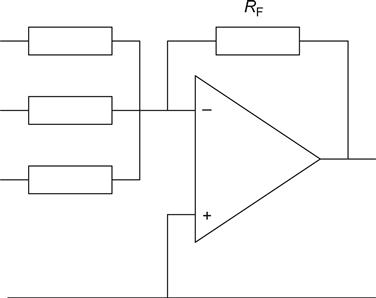
This circuit is known as the virtual earth adders and is most useful in bias servo circuits where we may need to add a number of correction signals. Voltage gain for each input may be determined using the inverter equation. When multiple inputs are driven, it is often best to determine the output voltage by summing the signal currents using Kirchhoff’s current law, finding the resultant current in RF and using Ohm’s law to determine the output voltage. This is not as tedious as it sounds.
The Non-Inverting Amplifier and Voltage Follower
Frequently, we need a non-inverting amplifier (see Figure 1.47).

In this configuration, we still have RF and RS, but the amplifier has been turned upside down, and the far end of RS is now connected directly to ground. Like the inverter we saw earlier, the amplifier has parallel-derived negative feedback, so its output resistance remains zero, but the feedback is now series-applied, making input resistance infinite. RF and RS now form a potential divider across the output of the amplifier, and the voltage at the inverting input is:
V(invertinginput)=RSRS+RF·Vout
Since the op-amp has infinite gain, the voltage at the inverting input is equal to that at the non-inverting input, which is Vin, so the gain of the amplifier is:
VoutV=RS+RFRS
If we now reduce the value of RF to zero and discard RS, the gain reduces to 1, and the amplifier is known as the voltage follower (see Figure 1.48).
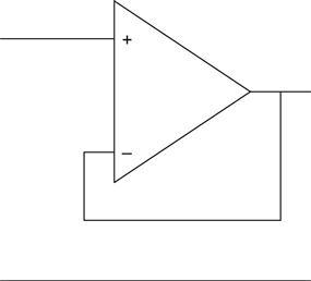
The voltage follower is an excellent buffer stage for isolating high-impedance circuits from low-impedance loads, and because it applies more negative feedback it is far superior to the single-transistor emitter follower that we saw earlier. (A very useful analytical technique is to treat an emitter follower as a common collector amplifier with 100% feedback and use the feedback equation to determine input and output resistances.) If we need more current than the op-amp can provide, we can add an emitter follower, or even a Darlington pair, to the output and enclose this within the feedback loop (see Figure 1.49).
The Integrator
This circuit is essentially an inverter with RF parallelled by CF, but if RF is omitted, it becomes an integrator and accumulates charge. The circuit may be considered to be a low-pass filter, in which case the cut-off frequency of the filter is:
f−3dB=12πCFRF
We can now see that if RF=∞, the cut-off frequency=0, and the amplifier has infinite gain at DC. Any DC offsets will gradually accumulate sufficient charge on the capacitor to cause the output of the op-amp to rise to maximum output voltage (±Vsupply), and the op-amp is then said to be saturated. For this reason, practical integrators are usually enclosed by a servo control loop. The servo error signal charges CF, but the loop aims to minimise the error, and so the voltage across CF tends to zero.
Again, we could sum several input currents if we wished, and one possible use of this circuit would be for monitoring the voltages across the cathode resistors of several output valves because the integrating function would remove the audio signal and provide a DC output voltage proportional to the total output valve DC current.
The Charge Amplifier
Noting that the voltage gain of the inverting amplifier was the ratio of resistances, there is no reason why those resistances should not be replaced by reactances. Although an amplifier with gain defined by inductances is neither practical nor useful, replacing the resistors with capacitors is useful and is known as a charge amplifier. Charge amplifiers are commonly associated with transducers such as condenser microphones and radiation detectors that change or produce a charge between the plates of a capacitor. Such sources thus look like a Norton source (pure current source in parallel with capacitance) and can be converted into a Thévenin source having a pure voltage source in series with the source capacitance. Connecting such a source directly to the inverting input of the amplifier produces a circuit very similar to the previously analysed resistive inverting amplifier (see Figure 1.50).
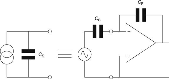
The significance of this arrangement is that the voltage gain is the ratio of two reactances and is independent of frequency. It is initially surprising that an amplifier employing capacitors should respond to DC but is easily proved by the assumption that the op-amp draws zero input current. If the op-amp does not draw input current, then any DC input current to the amplifier must pass through the feedback capacitor, causing the output to respond. Charge amplifiers are typically associated with small source capacitances (30 pF for a large-capsule condenser microphone) and require small feedback capacitances (2–3 pF is typical) to provide useful gain.
Like the integrator, practical charge amplifiers require a means of discharging the feedback capacitor to prevent amplifier saturation, and this is commonly achieved by a parallel discharge resistor (see Figure 1.51).
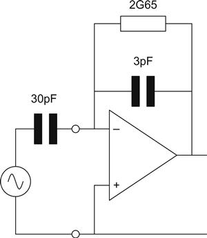
Unfortunately, the effect of adding the discharge resistor is to turn the amplifier into a differentiator. In audio terms, we have added a high-pass filter and would like to place its f−3 dB frequency as low as possible, certainly 20 Hz.
RF=12πf−3dBCF=12π×20×3×10−12=2.65GΩ
As the equation shows, charge amplifiers invariably require very large discharge resistances. Nevertheless, such resistors are readily available, even if they do require the wearing of clean cotton gloves when handling to avoid adding surface leakage currents.
Interestingly, because the charge amplifier responds to charge (or over the short term, currents), it is the noise current produced by the discharge resistor that is important, not its voltage. Remembering that the thermal noise voltage of a resistor is:
vnoise=√4kTBR
substituting into Ohm’s law gives:
inoise=√4kTBR
Thus, for lowest noise, the discharge resistor of a charge amplifier must be as large as possible.
DC Offsets
We briefly mentioned DC offsets when considering the integrator. Op-amps are not magical; they contain real transistors, and base, or leakage, current, known as bias current, will flow out of the inputs. The bias currents will not be perfectly matched, and the imbalance is known as offset current. The input transistors will not be perfectly matched for voltage either, so there will be an offset voltage between the inputs. These imperfections are detailed in the manufacturer’s datasheets and should be investigated during circuit design.