
Chapter 2
History of GPU Computing
Chapter Outline
To CUDA C and OpenCL programmers, GPUs are massively parallel numeric computing processors programmed in C with extensions. One does not need to understand graphics algorithms or terminology to be able to program these processors. However, understanding the graphics heritage of these processors illuminates the strengths and weaknesses of them with respect to major computational patterns. In particular, the history helps to clarify the rationale behind major architectural design decisions of modern programmable GPUs: massive multithreading, relatively small cache memories compared to CPUs, and bandwidth-centric memory interface design. Insights into the historical developments will also likely give readers the context needed to project the future evolution of GPUs as computing devices.
2.1 Evolution of Graphics Pipelines
Three-dimensional (3D) graphics pipeline hardware evolved from the large expensive systems of the early 1980s to small workstations and then PC accelerators in the mid- to late 1990s. During this period, the performance-leading graphics subsystems declined in price from $50,000 to $500. During the same period, the performance increased from 50 million pixels per second to 1 billion pixels per second, and from 100,000 vertices per second to 10 million vertices per second. While these advancements have much to do with the relentlessly shrinking feature sizes of semiconductor devices, they also come from the new innovations of graphics algorithms and hardware design innovations. These innovations have shaped the native hardware capabilities of modern GPUs.
The remarkable advancement of graphics hardware performance has been driven by the market demand for high-quality real-time graphics in computer applications. For example, in an electronic gaming application, one needs to render evermore complex scenes at ever-increasing resolution at a rate of 60 frames per second. The net result is that over the last 30 years, graphics architecture has evolved from a simple pipeline for drawing wireframe diagrams to a highly parallel design consisting of several deep parallel pipelines capable of rendering complex interactive imagery of 3D scenes. Concurrently, many of the hardware functionalities involved became far more sophisticated and user programmable.
The Era of Fixed-Function Graphics Pipelines
From the early 1980s to the late 1990s, the leading performance graphics hardware was fixed-function pipelines that were configurable, but not programmable. In that same era, major graphics Application Programming Interface (API) libraries became popular. An API is a standardized layer of software, that is, a collection of library functions that allows applications (e.g., games) to use software or hardware services and functionality. For example, an API can allow a game to send commands to a graphics processing unit to draw objects on a display. One such API is DirectX, Microsoft’s proprietary API for media functionality. The Direct3D component of DirectX provides interface functions to graphics processors. The other major API is OpenGL, an open-standard API supported by multiple vendors and popular in professional workstation applications. This era of fixed-function graphics pipeline roughly corresponds to the first seven generations of DirectX.
Direct Memory Access
Modern computer systems use a specialized hardware mechanism called direct memory access (DMA) to transfer data between an I/O device and the system DRAM. When a program requests an I/O operation, say reading from a disk drive, the operating system makes an arrangement by setting a DMA operation defined by the starting address of the data in the I/O device buffer memory, the starting address of the DRAM memory, the number of bytes to be copied, and the direction of the copy.
Using a specialized hardware mechanism to copy data between I/O devices and system DRAM has two major advantages. First, the CPU is not burdened with the chore of copying data. So, while the DMA hardware is copying data, the CPU can execute programs that do not depend on the I/O data.
The second advantage of using a specialized hardware mechanism to copy data is that the hardware is designed to perform copy. The hardware is very simple and efficient. There is no overhead of fetching and decoding instructions while performing the copy. As a result, the copy can be done at a higher speed than most processors can.
As we will learn later, DMA is used in data copy operations between a CPU and a GPU. It requires pinned memory in DRAM and has subtle implications on how applications should allocate memory.
Figure 2.1 shows an example fixed-function graphics pipeline in early NVIDIA GeForce GPUs. The host interface receives graphics commands and data from the CPU. The commands are typically given by application programs by calling an API function. The host interface typically contains a specialized DMA hardware to efficiently transfer bulk data to and from the host system memory to the graphics pipeline. The host interface also communicates back the status and result data of executing the commands.
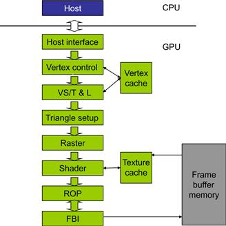
Figure 2.1 A fixed-function NVIDIA GeForce graphics pipeline.
Before we describe the other stages of the pipeline, we should clarify that the term vertex usually means the “corners” of a polygon. The GeForce graphics pipeline is designed to render triangles, so vertex is typically used to refer to the corners of a triangle. The surface of an object is drawn as a collection of triangles. The finer the sizes of the triangles are, the better the quality of the picture typically becomes. The vertex control stage in Figure 2.1 receives parameterized triangle data from the CPU. The vertex control stage converts the triangle data into a form that the hardware understands and places the prepared data into the vertex cache.
The vertex shading, transform, and lighting (VS/T&L) stage in Figure 2.1 transforms vertices and assigns per-vertex values (colors, normals, texture coordinates, tangents, etc.). The shading is done by the pixel shader hardware. The vertex shader can assign a color to each vertex but it is not applied to triangle pixels until later. The triangle setup stage further creates edge equations that are used to interpolate colors and other per-vertex data (e.g., texture coordinates) across the pixels touched by the triangle. The raster stage determines which pixels are contained in each triangle. For each of these pixels, the raster stage interpolates per-vertex values necessary for shading the pixel, which includes color, position, and texture position that will be shaded (painted) on the pixel.
The shader stage in Figure 2.1 determines the final color of each pixel. This can be generated as a combined effect of many techniques: interpolation of vertex colors, texture mapping, per-pixel lighting mathematics, reflections, and more. Many effects that make the rendered images more realistic are incorporated in the shader stage. Figure 2.2 illustrates texture mapping, one of the shader stage functionalities. It shows an example in which a world map texture is mapped onto a sphere object. Note that the sphere object is described as a large collection of triangles. Although the shader stage needs to perform only a small number of coordinate transform calculations to identify the exact coordinates of the texture point that will be painted on a point in one of the triangles that describes the sphere object, the sheer number of pixels covered by the image requires the shader stage to perform a very large number of coordinate transforms for each frame.
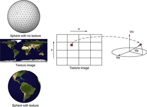
Figure 2.2 Texture mapping example: painting a world map texture image.
The ROP (raster operation) stage in Figure 2.2 performs the final raster operations on the pixels. It performs color raster operations that blend the color of overlapping/adjacent objects for transparency and anti-aliasing effects. It also determines the visible objects for a given viewpoint and discards the occluded pixels. A pixel becomes occluded when it is blocked by pixels from other objects according to the given viewpoint.
Figure 2.3 illustrates anti-aliasing, one of the ROP stage operations. There are three adjacent triangles with a black background. In the aliased output, each pixel assumes the color of one of the objects or the background. The limited resolution makes the edges look crooked and the shapes of the objects distorted. The problem is that many pixels are partly in one object and partly in another object or the background. Forcing these pixels to assume the color of one of the objects introduces distortion into the edges of the objects. The anti-aliasing operation gives each pixel a color that is blended, or linearly combined, from the colors of all the objects and background that partly overlap the pixel. The contribution of each object to the color of the pixel is to the amount of the pixel that the object overlaps.
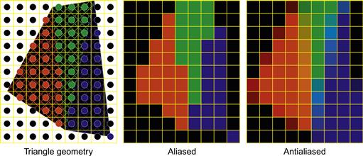
Figure 2.3 Examples of anti-aliasing operations: (a) triangle geometry, (b) aliased, and (c) anti-aliased.
Finally, the frame buffer interface (FBI) stage in Figure 2.1 manages memory reads from and writes to the display frame buffer memory. For high-resolution displays, there is a very high bandwidth requirement in accessing the frame buffer. Such bandwidth is achieved by two strategies. One is that graphics pipelines typically use special memory designs that provide higher bandwidth than the system memories. Second, the FBI simultaneously manages multiple memory channels that connect to multiple memory banks. The combined bandwidth improvement of multiple channels and special memory structures gives the frame buffers much higher bandwidth than their contemporaneous system memories. Such high memory bandwidth has continued to this day and has become a distinguishing feature of modern GPU design.
During the past two decades, each generation of hardware and its corresponding generation of API brought incremental improvements to the various stages of the graphics pipeline. Each generation introduced hardware resources and configurability to the pipeline stages. However, developers were growing more sophisticated and asking for more new features than could be reasonably offered as built-in fixed functions. The obvious next step was to make some of these graphics pipeline stages into programmable processors.
Evolution of Programmable Real-Time Graphics
In 2001, the NVIDIA GeForce 3 took the first step toward true general shader programmability. It exposed the application developer to what had been the private internal instruction set of the floating-point vertex engine (VS/T&L stage). This coincided with the release of Microsoft DirectX 8 and OpenGL vertex shader extensions. Later GPUs, at the time of DirectX 9, extended general programmability and floating-point capability to the pixel shader stage, and made texture accessible from the vertex shader stage. The ATI Radeon 9700, introduced in 2002, featured a programmable 24-bit floating-point pixel shader processor programmed with DirectX 9 and OpenGL. The GeForce FX added 32-bit floating-point pixel processors. These programmable pixel shader processors were part of a general trend toward unifying the functionality of the different stages as seen by the application programmer. NVIDIA’s GeForce 6800 and 7800 series were built with separate processor designs dedicated to vertex and pixel processing. The XBox 360 introduced an early unified-processor GPU in 2005, allowing vertex and pixel shaders to execute on the same processor.
In graphics pipelines, certain stages do a great deal of floating-point arithmetic on completely independent data, such as transforming the positions of triangle vertices or generating pixel colors. This data independence as the dominating application characteristic is a key difference between the design assumptions for GPUs and CPUs. A single frame, rendered in 1/60 of a second, might have 1 million triangles and 6 million pixels. The opportunity to use hardware parallelism to exploit this data independence is tremendous.
The specific functions executed at a few graphics pipeline stages vary with rendering algorithms. Such variation has motivated the hardware designers to make those pipeline stages programmable. Two particular programmable stages stand out: the vertex shader and the pixel shader. Vertex shader programs map the positions of triangle vertices onto the screen, altering their position, color, or orientation. Typically a vertex shader thread reads a floating-point (x, y, z, w) vertex position and computes a floating-point (x, y, z) screen position. Geometry shader programs operate on primitives defined by multiple vertices, changing them or generating additional primitives. Vertex shader programs and geometry shader programs execute on the VS/T&L stage of the graphics pipeline.
Pixel shader programs each “shade” one pixel, computing a floating-point red, green, blue, alpha (RGBA) color contribution to the rendered image at its pixel sample (x, y) image position. These programs execute on the shader stage of the graphics pipeline. For all three types of graphics shader programs, program instances can be run in parallel, because each works on independent data, produces independent results, and has no side effects. This property has motivated the design of the programmable pipeline stages into massively parallel processors.
Figure 2.4 shows an example of a programmable pipeline that employs a vertex processor and a fragment (pixel) processor. The programmable vertex processor executes the programs designated to the VS/T&L stage and the programmable fragment processor executes the programs designated to the (pixel) shader stage. Between these programmable graphics pipeline stages are dozens of fixed-function stages that perform well-defined tasks far more efficiently than a programmable processor could, and that would benefit far less from programmability. For example, between the geometry processing stage and the pixel processing stage is a “rasterizer,” a complex state machine that determines exactly which pixels (and portions thereof) lie within each geometric primitive’s boundaries. Together, the mix of programmable and fixed-function stages is engineered to balance extreme performance with user control over the rendering algorithms.
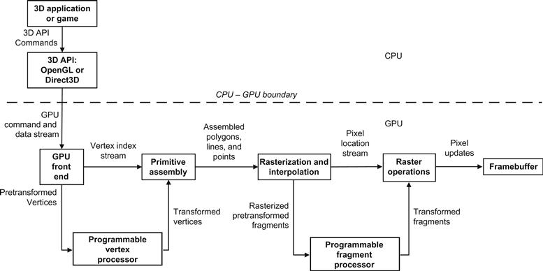
Figure 2.4 An example of a separate vertex processor and fragment processor in a programmable graphics pipeline.
Common rendering algorithms perform a single pass over input primitives and access other memory resources in a highly coherent manner. That is, these algorithms tend to simultaneously access contiguous memory locations, such as all triangles or all pixels in a neighborhood. As a result, these algorithms exhibit excellent efficiency in memory bandwidth utilization and are largely insensitive to memory latency. Combined with a pixel shader workload that is usually compute-limited, these characteristics have guided GPUs along a different evolutionary path than CPUs. In particular, whereas the CPU die area is dominated by cache memories, GPUs are dominated by floating-point data path and fixed-function logic. GPU memory interfaces emphasize bandwidth over latency (since latency can be readily hidden by massively parallel execution); indeed, bandwidth is typically many times higher than a CPU, exceeding 190 GB/s in more recent designs.
Unified Graphics and Computing Processors
Introduced in 2006, NVIDIA’s GeForce 8800 GPU mapped the separate programmable graphics stages to an array of unified processors; the logical graphics pipeline is physically a recirculating path that visits these processors three times, with much fixed-function graphics logic between visits. This is illustrated in Figure 2.5. The unified processor array allows dynamic partitioning of the array to vertex shading, geometry processing, and pixel processing. Since different rendering algorithms present wildly different loads among the three programmable stages, this unification allows the same pool of execution resources to be dynamically allocated to different pipeline stages and achieve better load balance.
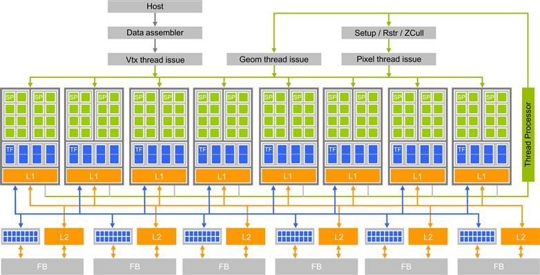
Figure 2.5 Unified programmable processor array of the GeForce 8800 GT graphics pipeline.
The GeForce 8800 hardware corresponds to the DirectX 10 API generation. By the DirectX 10 generation, the functionality of vertex and pixel shaders was to be made identical to the programmer, and a new logical stage was introduced, the geometry shader, to process all the vertices of a primitive rather than vertices in isolation. The GeForce 8800 was designed with DirectX 10 in mind. Developers were coming up with more sophisticated shading algorithms and this motivated a sharp increase in the available shader operation rate, particularly floating-point operations. NVIDIA pursued a processor design with higher operating clock frequency than what was allowed by standard-cell methodologies to deliver the desired operation throughput as area-efficiently as possible. High–clock speed design requires substantially more engineering effort, and this favored designing one processor array, rather than two (or three, given the new geometry stage). It became worthwhile to take on the engineering challenges of a unified processor (load balancing and recirculation of a logical pipeline onto threads of the processor array) while seeking the benefits of one processor design. Such design paved the way for using the programmable GPU processor array for general numeric computing.
2.2 GPGPU: An Intermediate Step
While the GPU hardware design evolved toward more unified processors, it increasingly resembled high-performance parallel computers. As DirectX 9–capable GPUs became available, some researchers took notice of the raw performance growth path of GPUs and they started to explore the use of GPUs to solve compute-intensive science and engineering problems. However, DirectX 9 GPUs had been designed only to match the features required by the graphics APIs. To access the computational resources, a programmer had to cast his or her problem into graphics operations so that the computation could be launched through OpenGL or DirectX API calls. For example, to run many simultaneous instances of a compute function, it had to be written as a pixel shader. The collection of input data had to be stored in texture images and issued to the GPU by submitting triangles (with clipping to a rectangle shape if that’s what was desired). The output had to be cast as a set of pixels generated from the raster operations.
The fact that the GPU processor array and frame buffer memory interface were designed to process graphics data proved too restrictive for general numeric applications. In particular, the output data of the shader programs are single pixels of which the memory location has been predetermined. Thus, the graphics processor array is designed with very restricted memory reading and writing capability. Figure 2.6 illustrates the limited memory access capability of early programmable shader processor arrays; shader programmers needed to use texture to access arbitrary memory locations for their input data. More importantly, shaders did not have the means to perform writes with calculated memory addresses, referred to as scatter operations, to memory. The only way to write a result to memory was to emit it as a pixel color value, and configure the frame buffer operation stage to write (or blend, if desired) the result to a 2D frame buffer.
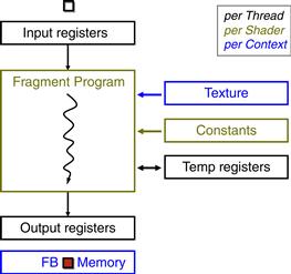
Figure 2.6 The restricted input and output capabilities of a shader programming model.
Furthermore, the only way to get a result from one pass of computation to the next was to write all parallel results to a pixel frame buffer, then use that frame buffer as a texture map as input to the pixel fragment shader of the next stage of the computation. There was also no support for general user-defined data types—most data had to be stored in one-, two-, or four-component vector arrays. Mapping general computations to a GPU in this era was quite awkward. Nevertheless, intrepid researchers demonstrated a handful of useful applications with painstaking efforts. This field was called GPGPU, for general-purpose computing on GPUs.
2.3 GPU Computing
While developing the Tesla GPU architecture, NVIDIA realized its potential usefulness would be much greater if programmers could think of the GPU like a processor. NVIDIA selected a programming approach in which programmers would explicitly declare the data-parallel aspects of their workload.
For the DirectX 10–generation graphics, NVIDIA had already begun work on a high-efficiency floating-point and integer processor that could run a variety of simultaneous workloads to support the logical graphics pipeline. The designers of the Tesla architecture GPUs took another step. The shader processors became fully programmable processors with instruction memory, instruction cache, and instruction sequencing control logic. The cost of these additional hardware resources was reduced by having multiple shader processors to share their instruction cache and instruction sequencing control logic. This design style works well with graphics applications because the same shader program needs to be applied to a massive number of vertices or pixels. NVIDIA added memory load and store instructions with random byte addressing capability to support the requirements of compiled C programs. To nongraphics application programmers, the Tesla architecture GPUs introduced a more generic parallel programming model with a hierarchy of parallel threads, barrier synchronization, and atomic operations to dispatch and manage highly parallel computing work. NVIDIA also developed the CUDA C/C++ compiler, libraries, and runtime software to enable programmers to readily access the new data-parallel computation model and develop applications. Programmers no longer need to use the graphics API to access the GPU parallel computing capabilities. The G80 chip was based on the Tesla architecture and was used in NVIDIA’s GeForce 8800 GTX. G80 was followed later by G92, GT200, Fermi, and Kepler.
Scalable GPUs
Scalability has been an attractive feature of graphics systems from the beginning. In the early days, workstation graphics systems gave customers a choice in pixel horsepower by varying the number of pixel processor circuit boards installed. Prior to the mid-1990s, PC graphics scaling was almost nonexistent. There was one option—the VGA controller. As 3D-capable accelerators appeared, there was room in the market for a range of offerings; for instance, 3dfx introduced multiboard scaling with the original SLI (scan line interleave) on their Voodoo2, which held the performance crown for its time (1998). Also in 1998, NVIDIA introduced distinct products as variants on a single architecture with Riva TNT Ultra (high performance) and Vanta (low cost), first by speed binning and packaging, then with separate chip designs (GeForce 2 GTS and GeForce 2 MX). At present, for a given architecture generation, four or five separate chip designs are needed to cover the range of desktop PC performance and price points. In addition, there are separate segments in notebook and workstation systems. After acquiring 3dfx, NVIDIA continued the multi-GPU SLI concept in 2004 starting with GeForce 6800, providing multi-GPU scalability transparently to both the programmer and to the user. Functional behavior is identical across the scaling range; one application will run unchanged on any implementation of an architectural family.
By switching to the multicore trajectory, CPUs are scaling to higher transistor counts by increasing the number of constant-performance cores on a die, rather than increasing the performance of a single core. At this writing the industry is transitioning from quad-core to oct-core CPUs. Programmers are forced to find four-fold to eight-fold parallelism to fully utilize these processors. Many of them resort to coarse-grained parallelism strategies where different tasks of an application are performed in parallel. Such applications must be rewritten often to have more parallel tasks for each successive doubling of core count. In contrast, the highly multithreaded GPUs encourage the use of massive, fine-grained data parallelism in CUDA. Efficient threading support in GPUs allows applications to expose a much larger amount of parallelism than available hardware execution resources with little or no penalty. Each doubling of GPU core count provides more hardware execution resources that exploit more of the exposed parallelism for higher performance. That is, the GPU parallel programming model for graphics and parallel computing is designed for transparent and portable scalability. A graphics program or CUDA program is written once, and runs on a GPU with any number of processors.
Recent Developments
Academic and industrial work on applications using CUDA has produced hundreds of examples of successful CUDA programs. Many of these examples are presented in GPU Computing Gems, Emerald and Jade editions [Hwu2011a, Hwu2011b] with source code available at www.gpucomputing.net. These programs often run tens of times faster on a CPU–GPU system than on a CPU alone. With the introduction of tools like MCUDA [SSH2008], the parallel threads of a CUDA program can also run efficiently on a multicore CPU, although at a lower speed than GPUs due to a lower level of floating-point execution resources. Examples of these applications include n-body simulation, molecular modeling, computational finance, and oil/gas reservoir simulation. Although many of these use single-precision floating-point arithmetic, some problems require double precision. The high-throughput double-precision floating-point arithmetic in more recent Fermi and Kepler GPUs enabled an even broader range of applications to benefit from GPU acceleration.
Future Trends
Naturally, the number of processor cores will continue to increase in proportion to increases in available transistors as silicon processes improve. In addition, GPUs will continue to go through vigorous architectural evolution. Despite their demonstrated high performance on data-parallel applications, GPU core processors are still of relatively simple design. More aggressive techniques will be introduced with each successive generation to increase the actual utilization of the calculating units. Because scalable parallel computing on GPUs is a still a young field, novel applications are rapidly being created. By studying them, GPU designers will continue to discover and implement new machine optimizations.
References and Further Reading
1. Akeley K, Jermoluk T. High-Performance polygon rendering. Proc SIGGRAPH 1988 1998:239–246.
2. Akeley K. RealityEngine graphics. Proc SIGGRAPH 1993 1993:109–116.
3. Blelloch GB. Prefix sums and their applications. In: Reif JH, ed. Synthesis of parallel algorithms. San Francisco: Morgan Kaufmann; 1990.
4. Blythe D. The direct3D 10 system. ACM Trans Graphics. 2006;25(3):724–734.
5. Buck I, Foley T, Horn D, et al. Brook for GPUs: Stream computing on graphics hardware. Proc SIGGRAPH 2004 2004:777–786 also Available at: <http://doi.acm.org/10.1145/1186562.1015800>.
6. Elder G. “Radeon 9700,” eurographics/SIGGRAPH workshop on graphics hardware. Hot3D Session 2002; Available at: <http://www.graphicshardware.org/previous/www_2002/presentations/Hot3D-RADEON9700.ppt>.
7. Fernando R, Kilgard MJ. The Cg tutorial: The definitive guide to programmable real-time graphics. Reading, MA: Addison-Wesley; 2003.
8. Fernando R, ed. Gpu gems: Programming techniques, tips, and tricks for real-time graphics. Reading, MA: Addison-Wesley; 2004; also Available at: <http://developer.nvidia.com/object/gpu_gems_home.html>.
9. Foley J, van Dam A, Feiner S, Hughes J. Computer graphics: Principles and practice, second edition in C Reading, MA: Addison-Wesley; 1995.
10. Hillis WD, Steele GL. Data parallel algorithms. Commun ACM. 1986;29(12):1170–1183 <http://doi.acm.org/10.1145/7902.7903>.
11. IEEE 754R working group. DRAFT standard for floating-point arithmetic P754. <http://www.validlab.com/754R/drafts/archive/2006-10-04.pdf>.
12. Industrial light and magic. OpenEXR 2003; Available at: <//www.openexr.com>.
13. Intel Corporation. Intel 64 and IA-32 Architectures Optimization Reference Manual 2007; Available at: <http://www3.intel.com/design/processor/manuals/248966.pdf>.
14. Kessenich J. The Opengl Shading Language, Language Version 1.20 2006; Available at: <http://www.opengl.org/documentation/specs/>.
15. Kirk D, Voorhies D. The rendering architecture of the DN10000VS. Proc SIGGRAPH 1990 1990;299–307.
16. Lindholm E, Kilgard MJ, Moreton H. A user-programmable vertex engine. Proc SIGGRAPH 2001 2001;149–158.
17. Lindholm E, Nickolls J, Oberman S, Montrym J. NVIDIA tesla: A unified graphics and computing architecture. IEEE Micro. 2008;28(2):39–55.
18. Microsoft corporation. Microsoft DirectX Specification, Available at: <http://msdn.microsoft.com/directx/>.
19. Microsoft Corporation. Microsoft directx 9 programmable graphics pipeline Readmond, WA: Microsoft Press; 2003.
20. Montrym J, Baum D, Dignam D, Migdal C. InfiniteReality: A real-time graphics system. Proc SIGGRAPH 1997 1997;293–301.
21. Montrym J, Moreton H. The GeForce 6800. IEEE Micro. 2005;25(2):41–51.
22. Moore GE. Cramming more components onto integrated circuits. Electronics. 1965;38 Available at <http://download.intel.com/museum/Moores_Law/Articles-Press_Releases/Gordon_Moore_1965_Article.pdf>.
23. Nguyen H, ed. GPU gems 3. Reading, MA: Addison-Wesley; 2008.
24. Nickolls J, Buck I, Garland M, Skadron K. Scalable parallel programming with CUDA. ACM Queue. 2008;6(2):40–53.
25. NVIDIA. CUDA Zone 2012; Available at: http://www.nvidia.com/CUDA.
26. NVIDIA. CUDA Programming Guide 1.1 2007; Available at: <http://developer.download.nvidia.com/compute/cuda/1_1/NVIDIA_CUDA_Programming_Guide_1.1.pdf>.
27. NVIDIA. PTX: Parallel Thread Execution ISA Version 1.1 2007; Available at: <http://www.nvidia.com/object/io_1195170102263.html>.
28. Nyland L, Harris M, Prins J. Fast N-Body simulation with CUDA. In: Nguyen H, ed. GPU gems 3. Reading, MA: Addison-Wesley; 2007.
29. Oberman, S. F.and Siu,M. Y. A high-performance area-efficient multifunction interpolator. Proc. 17th IEEE symp. computer arithmetic (pp. 272–279). Seattle Washington, 2005.
30. Patterson DA, Hennessy JL. Computer organization and design: The hardware/software interface 3rd ed. San Francisco: Morgan Kaufmann; 2004.
31. Pharr M, ed. GPU Gems 2: Programming techniques for high-performance graphics and general-purpose computation. Reading, MA: Addison-Wesley; 2005.
32. Satish, N. Harris, M. and Garland, M. Designing efficient sorting algorithms for proceedings of the 23rd ieee international parallel and distributed processing symposium. Rome, Italy, 2009.
33. Segal M, Akeley K. The opengl graphics system: A specification, version 2.1 2006; Available at: <http://www.opengl.org/documentation/specs/>.
34. Sengupta, S. Harris, M. Zhang, Y.and Owens, J. D. Scan primitives for GPU computing. Proc. of graphics hardware 2007 (pp. 97–106). San Diego, California, Aug. 2007.
35. Hwu W, ed. GPU computing gems, emerald edition. San Francisco: Morgan Kauffman; 2011.
36. Hwu W, ed. GPU computing gems, jade edition. San Francisco: Morgan Kauffman; 2011.
37. Stratton JA, Stone SS, Hwu WW. MCUDA: An efficient implementation of CUDA kernels for multi-core CPUs. The 21st International Workshop on Languages and Compilers for Parallel Computing 2008; [Canada; also Available as Lecture Notes in Computer Science].
38. Volkov V.and Demmel, J. LU, QR and cholesky factorizations using vector capabilities of GPUs. Technical Report No. UCB/EECS-2008-49, 1–11; also Available at: <http://www.eecs.berkeley.edu/Pubs/TechRpts/2008/EECS-2008-49.html>.
39. Williams S, Oliker L, Vuduc R, Shalf J, Yelick K, Demmel J. Optimization of sparse matrix-vector multiplication on emerging multicore platforms. Proc Supercomputing 2007 (SC’07) 2007. doi 10.1145/1362622.1362674 [Reno, Nevada].