Image sensors
INTRODUCTION
Photography has a long and well-documented history. The ability to record images in this manner has existed for more than 150 years. Less well known is that the electronic detection of light has also been possible for over a century and that images have been transmitted in this manner since the early 1900s. The growth of the digital imaging industry, therefore, should be attributed to something other than the use of electronics to form images.
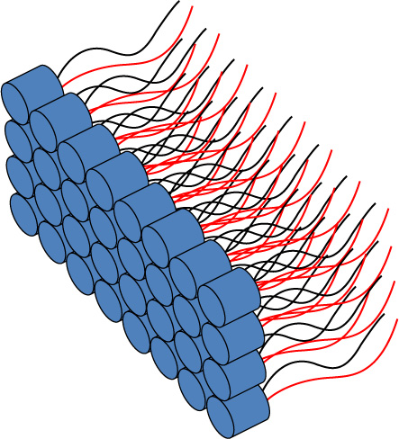
Figure 9.1 An array of photodiodes can be arranged to record an image.
Imagine using a simple photodiode to detect light. It is possible to arrange hundreds, or even thousands, of these in a grid to be able to record an image. However, the complexity of the wiring and the size of the photodiode (even if it were modest) make the proposition impractical (Figure 9.1). The invention of the integrated circuit and the process of large-scale integration addressed these wiring and organization problems by allowing the formation of many electronic components on a small area of silicon. It is this that facilitated modern digital imaging technology.
This chapter examines predominant electronic imaging sensors, the charge-coupled device (CCD) and complementary metal oxide semiconductor (CMOS) device, and their properties. Many differing types of electronic imaging sensors are available, far too many to include here. Therefore, those that principally detect visible light are concentrated upon and it is not considered appropriate to discuss thermal or high-energy detectors here.
MATERIALS AND DETECTION OF LIGHT
Imaging sensors rely heavily upon the properties of the materials of which they are comprised. The materials generally influence detection mechanisms, spectral sensitivity, noise characteristics and construction of a device. It is therefore useful to understand these fundamental mechanisms and their contribution.
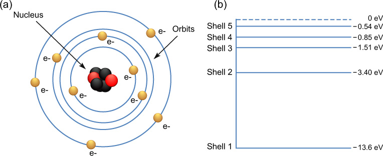
Figure 9.2 The Rutherford–Bohr model of the atom (a) and an energy level diagram (b).
Conductors, insulators and semiconductors
Over time, many models of the construction of atoms have been proposed. In 1913, Niels Bohr proposed that atoms consisted of a positive nucleus surrounded by negative electrons that could only occupy discrete orbits (Figure 9.2a). This was an improvement on an earlier model proposed by Rutherford in 1911 and is sometimes known as the Rutherford–Bohr model. Only a limited number of electrons may exist on each orbit and electrons may not exist at any orbits in between those for the atom. The number and position of the orbits depends on the element.
As has been mentioned in Chapter 2, electrons orbiting further from the nucleus have more energy. We may therefore imagine cutting a slice of Figure 9.2b to create an energy diagram, where the lower orbits have less energy and are ‘closer’ to the nucleus and those that are higher have more energy. To move between orbits, an electron must either lose energy to drop or gain energy to rise. If an orbit is full, electrons would not be able to join that orbit, and generally lower orbits fill first. An orbit may also be known as a shell or level.
Electrons will produce photons as they release energy, as has been seen in Chapter 2, and the wavelength of the light produced depends on the amount of energy released. If there is a large energy gap between two orbits, the electron will have to lose more energy and therefore the photon of light produced will have a shorter wavelength. If there are a discrete number of orbits for a given atom, it follows that only certain wavelengths of light will be produced. This is precisely the motivation behind Bohr’s model: to explain the line spectra produced by certain gases.
The valence band describes the orbit with the most energy that is normally occupied by electrons at absolute zero. These electrons generally have low energy levels. The empty band above the valence is known as the conduction band and contains free electrons which may conduct electricity as they are not tightly bound with the nucleus.
The energy difference between the valence and conduction band may differ for different types of atoms. If an electron does not gain sufficient energy to move from the valence band to the conduction band it will not become a free electron able to contribute to conducting electricity. The region between the valence and conduction band is sometimes referred to as the forbidden gap.
All materials may be classed as conductors or insulators, either allowing electricity to pass through them or not. Materials that have a high number of free electrons, those in the conduction band of a material, are generally good conductors, whilst insulators have few or no electrons that are able to escape the valence band. The electronic properties of elements, the manner in which they combine to form molecules and external application of energy or force influence the number of free electrons in a material and their mobility. Generally an insulator has a larger forbidden gap between the valence and conduction bands.
A semiconductor is a material that has conductivity in between an insulator and a conductor. Its conductivity is closer to that of an insulator in a natural state and few electrons gain enough energy to reach the conduction band. By applying energy, it is possible to excite increasing numbers of electrons into the conduction band and increase the conductivity of the material. Energy may be applied by heating, or by applying light or non-visible radiation and in some cases mechanical forces. Silicon and germanium are common semiconductors, though a large number of other materials and compounds are used, such as silicon germanium, gallium arsenide and indium phosphide.
Being able to modify the conductivity of a semiconductor has made them immensely important in the technology industries and they have had a tremendous impact on the world. Integrated circuits (computer chips), light-emitting diodes (LEDs), diodes, transistors and a host of other devices all rely on the use of semiconductors. It is very difficult in modern society to find a device that doesn’t have a semiconductor in it.
Doping
The four outermost electrons in silicon and germanium may form covalent bonds with four neighbouring atoms to form a perfect crystal lattice. Because all of these electrons are involved with forming the crystal structure, they cannot conduct electricity. In their natural state, therefore, silicon and germanium do not conduct electricity well. The electronic properties of silicon and other semiconductors, however, may be modified using a process termed doping. Doping is the introduction of varying quantities of impurities into the semiconductor to change the conductivity. A doped semiconductor is commonly referred to as an extrinsic semiconductor.
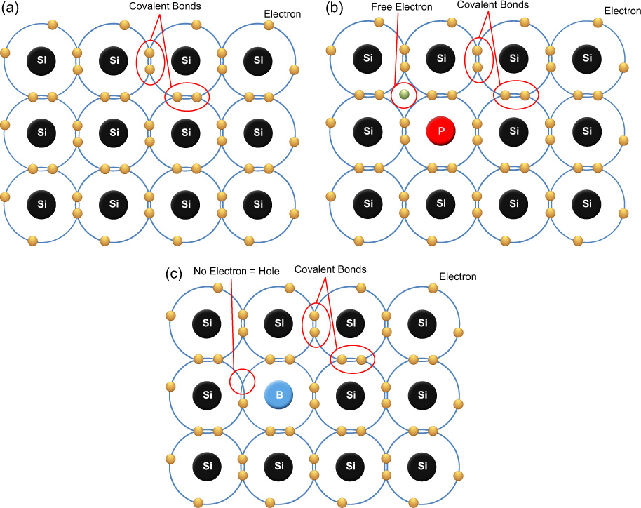
Figure 9.3 Silicon (a), N-type (b) and P-type (c) silicon electron diagrams. The silicon forms covalent bonds to form a perfect lattice. The addition of phosphorus produces a free electron, the addition of boron a hole.
There are essentially two types of doping: N-type and P-type. Both permanently increase the conductivity of the semiconductor, though not by very much and using slightly different methods.
To understand the role of a dopant, the properties of both the dopant and the base material must be considered (Figure 9.3). Dopants are usually classified as either acceptors or donors. Donor dopants, or N-type dopants, donate weakly bound electrons to the valence band when incorporated into the otherwise pure crystal lattice. These electrons may be excited into the conduction band very easily, enabling the conductivity to increase. The majority carrier of the electricity is therefore negative electrons, hence the name N-type. Arsenic, antimony and phosphorus may all be used as N-type dopants. Each has five electrons in the valence band and therefore has an electron left over when bound to the valence four silicon.
Acceptor donors produce positive holes as majority carriers. Valence three materials, such as boron, are added and, once incorporated into the semiconductor lattice, accept electrons easily. The valence four silicon can form only three bonds with the acceptor material and therefore an electron is missing in the lattice. We can think of this missing electron as a positive hole. Electrons from other atoms can fill this hole, but that in turn creates a hole somewhere else. We can think of the hole as being able to move throughout the material, conducting electricity as it does so. Just like electrons, holes may be attracted or repelled by opposite or like charges.
If large amounts of impurities are added the semiconductors will become good conductors and may be used as the replacement for wires in some integrated circuits. Electric fields are created at the junctions between N- and P-type semiconductors, causing electrons and holes to migrate away from them. It is the utilization of this effect that allows the production of transistors, diodes and many other electronic components (Figure 9.4).
Photoemission and photoabsorption
When electrons move from one energy level to another in a material they may only do so by the absorption or release of energy (see Chapter 2). An electron moving from the conduction band of a material to the valence band needs to lose energy and, as a consequence, often produces quanta of energy. If the amount of energy released is sufficient, this will be seen as a photon of visible light. The equation governing the relationship of energy released is given by Eqn 2.35 in Chapter 2. It is this principle that governs light-emitting diodes and solid-state lasers. Conversely, if light of sufficient energy is absorbed by a semiconductor it may excite an electron from the valence band into the conduction band, consequently leaving a positive hole, a process known as electron–hole pair generation.
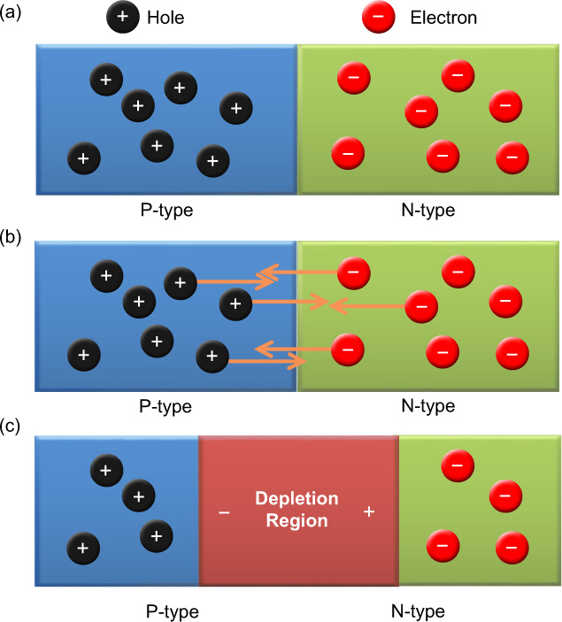
Figure 9.4 A P–N junction (a) and its depletion region formed as holes and electrons diffuse across the junction (b), to produce an electric field (c).
Diodes
A diode allows electrical current to flow in one direction but not the other and is one of the simplest devices that may be constructed from semiconductors. Amongst other things, they may be used to protect electronics from electricity with the wrong polarity. A diode is formed from the junction between N- and P-type semiconductors (Figure 9.4a). At the junction, the weakly bound electrons from the N-type material migrate to fill the holes in the P-type (Figure 9.4b). As electrons have moved from the N-type to the P-type material, the N-type becomes slightly positively charged and the P-type negatively charged in the region about the junction. This is known as the depletion region because there remain very few electrons and holes (Figure 9.4c).
The size of the depletion region may be influenced by applying a voltage. Operated in reverse bias, applying a positive voltage to the N-type and negative to the P-type, the depletion region increases and the net conductivity across the junction decreases. Applying a forward bias, i.e. a positive voltage, to the P-type and negative to the N-type, the depletion region decreases and the conductivity across the junction increases. Diodes are generally not perfect and a small current is generally conducted in the reverse bias mode. In forward bias mode, a small positive voltage is needed (≈ 0.7 volts) before the diode will conduct a useful current.
Transistors
Transistors are a natural extension of diodes. Using three layers of silicon, a PNP or NPN sandwich may be created. In either case, two P–N junctions are effectively created, blocking current from flowing in any direction. Applying a small voltage to the central portion can then control the current flow through the device, turning it on and off. The switching current may be many times less than the current it controls. A switch is a fundamental component of any computer and is a building block of logic and Boolean operations. Using photolithography, it is possible to fit millions of transistors on to a piece of silicon, thereby creating the tiny, complex circuitry that modern devices rely upon.
CCD and CMOS sensors
Charge-coupled device (CCD) and complementary metal oxide semiconductor (CMOS) sensors are similar in their architecture and function. They both utilize semiconductor technology to collect an image focused by a lens on to them. Some of the differences between the technologies will be detailed as we progress through this chapter, but the majority of concepts may be applied to both technologies.
Trying to conceive of a new type of memory for computers, CCDs were invented, almost by accident, by Willard Boyle and George Smith at Bell Laboratories in 1969. CCDs therefore precede CMOS devices and are a more mature technology. CMOS devices initially suffered from high noise and therefore low image quality, though these arguments are not as valid in the present day. CCD sensors are generally used for higher quality imaging and scientific applications, such as astronomy, whereas CMOS technology is used in many devices from cellphones and ‘webcams’ to prosumer digital single-lens reflex (ProDSLR) cameras and security devices. The pricing of the devices has fallen considerably as the technologies have matured and digital devices have become extremely common. The sales of digital cameras have surpassed those of film cameras since the last edition of this book.
Both CMOS and CCD imaging sensors are constructed from the same material, silicon, and this gives them fundamentally similar properties of sensitivity in the visible and near-IR spectrum. Sensors are formed on silicon wafers and cut apart, generally with a diamond saw, to produce individual sensors or die. CCD and CMOS sensors can support a variety of photoelements, though the fundamentals are primarily concentrated upon here.
MOS capacitor
At the heart of the CCD is the metal oxide semiconductor (MOS) (Figure 9.5). It is comprised of silicon doped with impurities, such as aluminium, to produce a P-type semiconductor, formed on a silicon substrate. Above the P-type semiconductor is formed a gate from polysilicon, which is held at a positive bias and produces a depletion region in the semiconductor. Generally, three or four such photogates are used in a single pixel to enable charge transfer (see later).
Silicon has a band gap of 1.1 eV; this is the energy required to promote one of its valence electrons to its conduction band (Figure 9.6). Using the relationship expressed in Eqn 2.35 it is therefore found that it has an inherent sensitivity up to approximately 1100 nm. While this may be an advantage for recording in the IR region of the spectrum for security and other applications, it is a disadvantage for imaging within the visible region of the spectrum and results in incorrect tone and colour balance. Image sensors to be used in the visible region of the spectrum have an IR filter to restrict their response to the visible region below approximately 670 nm.
The positive voltage to the gate (Vgate) causes mobile positive holes to migrate to the ground electrode, creating a depletion region. When light of sufficient energy (greater than 1.1 eV) is absorbed in the depletion region an electron–hole pair is produced. The electron remains in the depletion region whilst the positive holes migrate to the ground electrode. If the positive voltage was not applied, the hole and the electron would recombine and release energy in the form of heat.
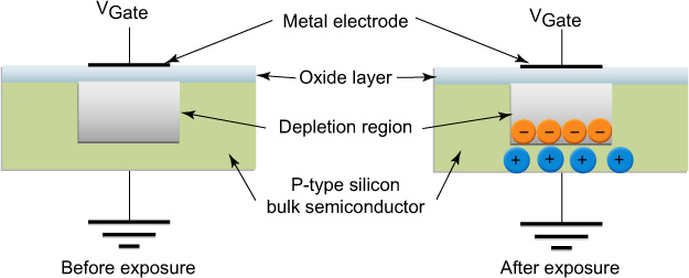
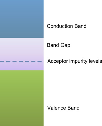
Figure 9.6 A representation of the band gaps in silicon.
The number of electrons that can be retained in the depletion region is the well capacity, which depends on the physical sizes of the oxide layer and the gate electrode area, as well as the applied voltage.
Photodiodes
CMOS sensors employ photodiodes in a variety of configurations as opposed to MOS capacitors. The photodiode is formed by creating a layer of N-type silicon in contact with the P-type. This creates the depletion region, rather than employing a bias provided by a polysilicon gate.
As for the MOS capacitor, a photon may be absorbed in the depletion region to create an electron–hole pair and the device is subject to the same constraints of well capacity. To increase the sensitivity of the photodiode, a layer of intrinsic semiconductor may be placed between the P–N junction to create a P–I–N diode or pinned photodiode. The layer of intrinsic semiconductor effectively increases the full-well capacity of the photodiode.
Variations in CMOS pixel architecture relate additionally to readout and amplification mechanisms and are discussed later.
In reality, CCD and CMOS architectures may use photodiodes and photogates interchangeably and mechanisms to read out the image formed remain the main distinguishing feature between the two technologies.
Pixels
In order to record images the sensor contains a large number of elements (pixels) in the form of a two-dimensional array for most CCD and CMOS cameras and a linear array for scanning devices and some types of large-format studio cameras. Generally, the individual pixels are separated from each other by infusing the substrate with boron or a similar element to create channels in a grid pattern on the substrate. Sensor sizes, numbers of picture elements and the bit depth (i.e. number of possible grey levels) are all increasing rapidly as technologies develop and this is commented upon later, though 12 million pixels (megapixels or Mp) are readily available at a reasonable cost for consumer cameras at the time of writing. A common pixel size is currently 1.75 mm, with 1.4 mm being introduced. At least one company at the time of writing has announced pictures that have been generated with a 1.1 mm pixel sensor prototype.
As will be seen later, a number of other layers may exist on top of the basic sensor, including a Bayer array, micro-lenses and infrared reflecting filters.
CCD AND CMOS IMAGE READOUT
A fundamental difference between CCD and CMOS technologies is the manner in which the signal is read from the pixels on the sensor. The CCD gets its name from the method of moving the stored image across the sensor (charge coupling) and reading it out at one corner, whereas each pixel in a CMOS device contains several components and may be read individually in most architectures.
CCD readout
Exact architectures may vary, though generally each pixel in a CCD is subdivided with three photogates. The charge may be thought of as gathering under the photogate to which the highest potential is applied. Adjustments of the gate voltages then allow transfer of electrons from well to well as a function of time. Figure 9.7 shows the way in which charges are transferred between neighbouring wells (1). After exposure to light, the charge in well one is shown in (2). If a voltage is applied to gate 2, electrons flow from well 1 to well 2 (3) until equilibrium is reached (4). If the voltage to gate 1 is reduced, electrons begin to be completely transferred to well 2 (5 and 6); complete transfer is shown. Thus, charges are transferred in a time-dependent way if one considers a complete array of image elements and their gates. The clocking sequence for a three-phase device is shown in Figure 9.8. It may be seen that only one-third of the pixel area is available as the well capacity (three gates). Both two- and four-phase readout architectures also exist. By repeating the above procedure it is possible to shift the charge as many times as desired.
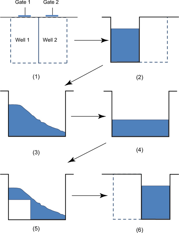
Figure 9.7 Charge transfer in a CCD.
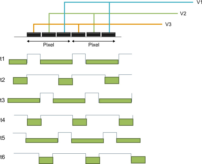
Figure 9.8 Clocking sequence for a CCD.
By combining corresponding electrodes of complete rows the individual charges for the whole image may be shifted down by a row at the same time (Figure 9.9). The charges at the bottom of the sensor are transferred into a serial readout register. The serial readout register works in a manner similar to the CCD itself and is able to shift the charge in each pixel towards the amplification and analogue-to-digital converter (ADC) circuitry. The ingenious method of charge transfer in the CCD may also be considered a disadvantage as it is essentially rendered a serial device. The ADC becomes a bottleneck, only able to digitize one value at a time, albeit very quickly.
During each shift of the stored charge, a small number of electrons may be left in the potential well. The efficiency at which this process may be completed is known as the charge transfer efficiency. Charge transfer efficiency is generally very high (>99.999%) and is usually dependent upon the speed at which the transfer is completed. Faster transfers tend to leave little time for straggling electrons. The effect is also cumulative; the charge packets at point A in Figure 9.9 have more transfers to complete than those at B and are therefore more susceptible to the effects of charge transfer.
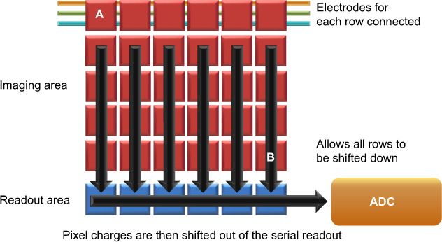
Figure 9.9 Basic architecture for transferring a full-frame image from a CCD.
There are a number of different ways in which CCDs may be configured for different readout architectures, each with its own advantages and disadvantages. Some different architectures are given in Figure 9.10, including full frame, frame transfer and interline transfer.
The full-frame configuration shown in Figure 9.10a is generally the simplest and most sensitive, as it devotes the most area to image capture. If nothing is done to shield the CCD from light during the readout phase, charge will continue to accumulate on the device and smearing of the image will occur. Therefore, these devices may only realistically be used with an external mechanical shutter to shield the sensor during readout. Due to their high sensitivity and use of a shutter these devices are most appropriate for DSLRs and similar cameras.
Frame transfer CCDs overcome the issues of mechanical shuttering by providing a ‘storage’ area on chip which is shielded from light. Whilst they still suffer from smear, the transfer of the image can be completed very quickly as the constraint of the serial readout has been changed. Once the image is in the storage area it may be clocked out during the exposure of the next frame. This increases the duty cycle of the sensor as more time may be devoted to collecting light. In addition, the frame rate is higher than that of a mechanically shuttered CCD and issues associated with mechanical wear and vibration are reduced. These sensors are more expensive as the area of silicon needed to produce them is double that of the full frame.
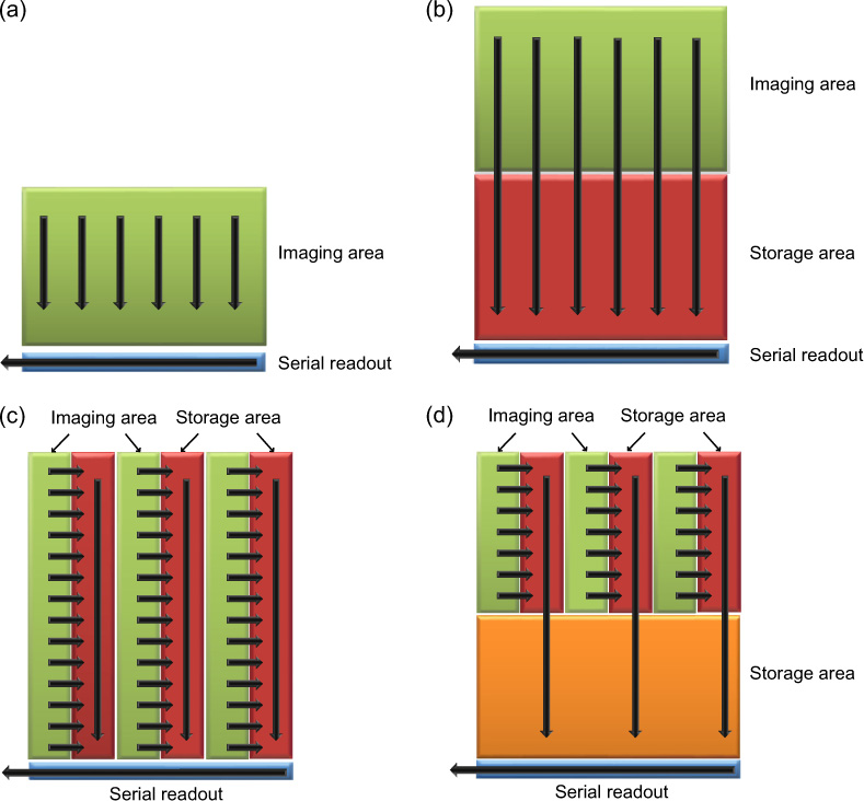
Figure 9.10 Readout architectures for CCDs. (a) Full frame, usually used with a mechanical shutter. (b) Frame transfer. (c) Interline transfer. (d) A hybrid interline transfer device with a storage area.
Interline transfer devices have shield strips between light-sensitive ones to reduce the effect of smear even further, also increasing duty cycle and frame rate. The addition of the shielded strips lowers the fill factor of the sensor and a microlens array is generally added to compensate for this. In addition, the MTF of the sensor may be different in the vertical and horizontal directions (Chapter 7). The complexity of the sensor can lead to increased costs.
CMOS readout
The architecture of CMOS sensors differs significantly from that of CCDs in terms of the manner in which the signal is read. Dependent upon the architecture, each pixel in a CMOS sensor has its own set of transistors to perform amplification and to assist with readout and reset. By including circuitry to select columns and rows, entire columns or rows can be read out simultaneously. Figure 9.11 shows an early passive pixel architecture. The readout transistor for each pixel in combination with the horizontal and vertical readout circuits allows each pixel to be individually addressed. Adding amplification to each pixel allows readout noise to be overcome, creating the active pixel sensor (Figure 9.12).
As separate amplifier and reset transistors are used for each pixel, CMOS sensors tend to have increased levels of noise over CCDs, as matching these components is a challenge and the photodiode resets to a slightly different value each time. The sophistication of a photodiode-based pixel is related to the number of transistors that can be incorporated into each pixel. The predominant architecture as of writing is three transistor designs (3T) consisting of the photodiode, reset, addressing and source-following components. A number of 4T, 5T and 6T designs exist, reducing read out and reset noise.
Advances in technology over the past decade have significantly reduced the gap with CMOS as the predominant sensor in the consumer market.
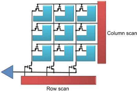
Figure 9.11 Passive pixel CMOS sensor.
Because of the extra area needed to accommodate the circuitry for each pixel, the fill factor and the sensitivity of the CMOS device suffer. CMOS sensors may be made using similar silicon foundry technology to computer memory and other integrated circuits and, hence, they may accommodate image processing and other circuitry that traditionally gets put into supporting chips for CCD devices. This allows for the production of sophisticated devices and full ‘camera-on-chip’ imagers are regularly seen at the time of writing. However, this extra complexity can increase design time and updates to the sensor’s on-chip functions may often require revision of the chip design.
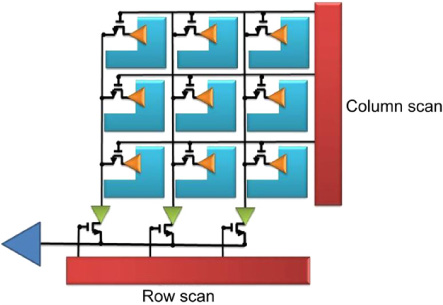
Figure 9.12 Active pixel CMOS sensor.
Though the CMOS sensor requires less off-chip support it uses a larger area of silicon for the supporting processing, and the cost benefits of using the same or older depreciated foundries for production have not been as large as expected. CCDs, by comparison, require dedicated foundries and little, if anything else at all, can be produced. Because a CCD uses a single amplifier and ADC, the uniformity of these processes is very good.
The method of reading the CMOS sensor allows for windowing of the image, selecting a reduced portion of the device from which to read an image. This, in turn, allows frame rates to increase as only part of the available data is read. In addition, control of the imaging parameters can be performed on a frame-by-frame basis, making the device highly configurable.
CMOS sensors generally consume less power than CCDs, which need accurate timing circuitry. CMOS sensors are therefore a preferred choice for consumer goods where battery life is important, e.g. small cellphones and cameras. As with many commercial products, the choice between the sensors is a compromise between cost, performance, efficiency and suitability for purpose.
AMPLIFICATION AND ANALOGUE-TO-DIGITAL CONVERSION
The voltage formed at each photosite is tiny, of the order of femtovolts, and requires amplification before it can be converted into a digital number and subsequent use in a computer. As has been seen, where the amplification occurs is a difference between CCD and CMOS devices.
Because of the inherent spectral sensitivity of the materials from which the device is made, the total charge collected for each wavelength of light will be different even if presenting a spectrally uniform test target to the sensor. Therefore, if a colour image is produced by collecting red, green and blue light with one of the methods mentioned in the later sections, it will display a colour bias. This colour bias is further compounded by the relative transmittance of each of the filters used to divide the spectrum into its colour constituents. As is seen in other chapters, alternatives to red, green and blue may be used.
The amplification of the signal from each of the colour channels may be used to correct for the difference in the relative sensitivity of each. By amplifying the less sensitive channels more, the amplitude of the signals from each may be matched. Further, as with photographic emulsions, a colour shift may be seen when different illumination is used (see Chapter 3). Generally, incandescent lights appear ‘warmer’ and daylight appears ‘cooler’. Using processing within the digital camera, the illuminant type may be detected. This information may then be used to adjust the analogue gain to correct the white balance of the sensor. The advantage of using this method is that no ‘rounding errors’ occur, as would be the case when applying amplification using integer maths after the signal is digitized. Some digital amplification may exist in cameras in addition to analogue amplification to enable other tasks.
Noise in the sensor is related in part to the signal level detected on the sensor. Therefore, it should be noted that for those channels in which the sensitivity is lower and the subsequent amplification higher, the noise in those channels will also be amplified and will be higher. Therefore, it is necessary when testing colour digital sensors to characterize the noise and signal characteristics of each channel.
After amplification, the signal is converted into a digital number using an analogue-to-digital converter (ADC). There are two basic methods of digitizing a signal: dual slope integration and successive approximation. Dual slope integration is slower, though less noisy than successive approximation. Successive approximation sequentially generates ‘guess’ voltages and compares them to the signal being digitized. The first ‘guess’ represents the first bit and is exactly half of the ADC input range. If the signal to be digitized is higher the bit is set to 1 and lower it is set to 0. The next voltage is a quarter of the input range and added to the result of the first guess. Again, if the signal is higher the next bit is set to 1 and if it is lower, to 0. The third guess is one-eighth of the input range and so on until a guess is made for each bit corresponding to the bit depth of the ADC. A slope integration ADC integrates (collects) the input voltage and times how long it takes to reach a reference voltage. The time is proportional to the input voltage. This method, however, is subject to manufacturing tolerances of the components. A dual slope integration ADC integrates the input as in the first case for a known amount of time, then times a discharge with respect to a known voltage. The time of discharge is proportional to the input voltage. As the same components are used to integrate and discharge the signal, the result is not subject to error caused by component tolerances.
The readout rate, the time in which an image has to be ‘read’ from the sensor, determines the time for which each pixel has to be read from the chip and digitized. Generally, the less time that a pixel has to be read from the sensor, the more noise is introduced into the measurement.
The scale that an ADC has to work with depends upon the number of bits available to store the signal. A bit is the most basic digital representation available, known as binary, and may take the value 0 or 1. The total number of levels that can be represented is given by 2b, where b is the number of bits. Therefore, an 8-bit ADC can create 28 or 256 levels. Conventionally, these levels start at 0 and go to 2b − 1, or 0 to 255 in this example. The significance, or importance, of each bit when written in binary varies with its position and the proportion of the signal it represents (Figure 9.13). The digit on the right is known as the least significant bit (LSB) as it represents the smallest component the ADC can convey. The left-hand digit is known as the most significant bit (MSB).
The task of the ADC is to choose the value that most closely matches the input signal. Say the input signal lies between 0 and 3 volts and the ADC is 8 bits. Zero volts will be assigned a digital value of 0, 3 volts will be assigned a value of 255, 1.5 volts would be assigned to 127, etc. This may be represented as a graph (Figure 9.14).

Figure 9.13 Binary number representation.
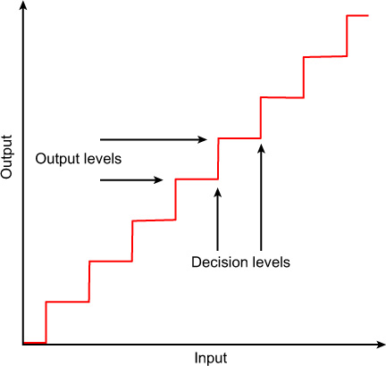
Figure 9.14 Decision levels for an analogue-to-digital converter.
The range of the ADC is divided into decision levels and output levels and shows how the input signal is assigned to the output.
When digitizing a signal, error occurs because of the resolution of the ADC. If the signal has a value halfway between two output levels, the ADC has to digitize it to either the value above or below it. This creates an error of 0.5LSB. As the number of bits with which to represent the signal increases, the relative size of the LSB becomes smaller. For an 8-bit ADC the LSB represents 1/256th of the input; for 10-bit ADC the LSB represents 1/1024th of the input signal. Therefore, using higher bit depths results in smaller errors when digitizing an image.
In addition to ADC error, there exists ADC noise (see Chapter 24). Using the 0–3 volt signal and 8-bit ADC as before, a value of 1.5 volts should be digitized as 127. However, sometimes the ADC will give 126, or 125, maybe 128 or 129. This is a random component that depends upon the quality of the ADC and the time available to digitize the value. Generally, the noise in an ADC will be quoted as a fraction of the LSB, e.g. 8 bits ± 0.25LSB. A fraction of an LSB may be used as this is the average error over a large number of measurements.
Because of these errors, information is lost at the point at which an image is digitized and some noise is introduced.
The image digitized from the sensor is used as input into an image-processing pipeline consisting of many stages designed to enhance the quality of the image before it is available for the user. The image-processing pipeline is discussed in more detail in the section on digital cameras in Chapter 14. Such processing could include colour correction, gamma correction, demosaicing, noise reduction, defect masking and a number of others. Performing mathematics on integer numbers, however, produces rounding errors. As digitization of the image on an image sensor is the first in many image-processing stages, it is generally digitized to a much higher bit depth than will be required for final output to a computer in order to reduce these errors. An image-processing pipeline within a digital camera may operate at 12–20 bits for a final output of 8–10 bits.
The number of intensity levels that can actually be resolved in the final image depends largely upon the noise in the sensor and the mode of operation. Because an image may be digitized at 10 bits, distinguishing 1024 distinct levels may not be possible (refer to Chapter 24 for further information). Generally, low light, high ISO, high frame rate, multispectral and poor f-number will be the type of factors that can increase image noise. The aperture, or f-number, of a lens is given by the ratio of the focal length to the aperture diameter (Chapters 6 and 10). A poor f-number (i.e a large f-number) lens will produce a darker image and larger Airy disc, increasing the exposure time and decreasing resolution. Further aspects of amplification and digitization are discussed in the following section.
SCANNING METHODS
Sensors may be deployed in a large variety of sizes from tens of pixels in devices such as optical mice to large linear arrays for scanners and studio cameras. The exact size depends upon the format of the device and the application. There are three basic scanning methods to utilize sensors in the most economical way: point scanning, line scanning and area scanning (Figure 9.15).
Point scanning uses a single pixel array and scans this throughout the full field of view. In practice the scanning is usually achieved optically, using a faceted mirror or fast and slow scan mirrors. Whilst the output from the device is generally very uniform because a single imager is used, it can often suffer from mechanical defects in the scan mechanisms. Linear arrays are often used in flatbed scanning, consisting of a strip of pixels, generally a few pixels deep and a number of thousands wide. By scanning this along its short direction it is possible to quickly build an image of a document. Some large-format studio cameras also use this technique. The scanning mechanics are simpler and the registration issues are reduced in one direction. Colour may be generated in a number of ways, as is shown later. Both of the above methods may only be used on static subjects, as any movement will cause image smear. Area scanning usually refers to a staring array, so called because it has no moving parts. The lack of scanning means that higher frame rates and relative sensitivities can be achieved.
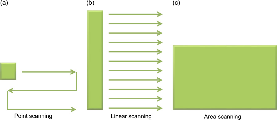
Figure 9.15 Point (a), line (b) and area scanning (c) approaches.
IMAGING PERFORMANCE
Performance trade-offs
Many of the performance characteristics of a sensor are linked. Inevitably, if one measure increases another will often decrease. Common terms for sensor performance measures are given in Table 9.1. These are expanded upon in this and later chapters. Silicon wafers are technologically expensive to produce but the abundance of digital cameras has made them a commodity, driving prices down. The useful area upon each silicon wafer is expensive. As sensor sizes are reduced, each wafer can produce more. If sensor size is halved, wafers can produce four times as many. Therefore, pixel size, sensor size and cost are important factors, which in turn have an effect on image quality.
Common sensor sizes range from 1/10″ to 4/3″ and are specified as the length of the diagonal. The aspect ratio is commonly 4:3, though the recent introduction and proliferation of high definition television (HDTV) has seen an increase in the use of 16:9. A few high-quality image sensors exist that have 35 mm and square aspect ratios.
The size of the image sensor affects the apparent focal length of the lens used with the system. Many photographers familiar with the 35 mm format understand that a ‘standard lens’ has a focal length of 50 mm, a standard lens being a focal length that gives a field of view approximately similar to that of the eye. A practitioner of medium-format photography will likewise exclaim that a standard lens is 80 mm. If a smaller sensor than those commonly employed in film camera formats is used, it has the effect of cropping the image and, if the resultant image is displayed at the same size, will increase the apparent focal length of the lens.
The effect that this has on users of DSLR cameras is that the focal length of a lens should be multiplied by a factor to find its 35 mm equivalent (often termed the ‘effective focal length’). The diagonal of a 35 mm frame is approximately 43 mm. Using a 1″ imager will result in a crop factor of ×1.7. Thus, a 100 mm lens will have an apparent focal length of 170 mm. Producing smaller sensors generally reduces the size and weight of the optical systems that are needed to accompany them because of the above scaling. However, lens placement and tolerancing become increasingly critical as the resolution requirements of the system generally become higher.
The size of the sensor and the number of pixels contained on that sensor specifies the physical limitations on the size of an individual pixel. As each pixel gets smaller, the number of electrons that it can trap, known as the full well, decreases and is related to its area. Thus, the full well of a 2 mm pixel will be a quarter of the size of a 4 mm. The full well and the various sources of noise in the sensor will define the dynamic range of the device. This is generally given as:
where f is the number of electrons in the full well and nRMS is the root mean squared noise of the device in the dark. Thus, a device with a full well of 21,000 and RMS noise of seven electrons respectively would have dynamic range of 3000:1 or 69.5 dB (see Chapter 24 for various sources of noise).
The response of a CCD or CMOS device is generally highly linear (Chapter 24). However, as the full well approaches capacity, its ability to store more charge diminishes until the point at which it becomes saturated. Therefore, when plotting a graph of relative responsivity versus exposure (Figure 9.16), one finds that as a pixel approaches saturation its sensitivity decreases and then drops dramatically. The linear full well is usually chosen to represent the linear portion of the output of the device and is a trade-off between the non-linearity that can be tolerated maximizing the dynamic range of the sensor. Amplification of the signal must also be taken into consideration as it will lower the dynamic range of the signal, increasing the levels of noise.
Table 9.1 Common performance terminology for digital sensors
CHARACTERISTIC |
COMMENT |
Detector size |
Dimensions of sensor area (mm × mm) |
Pixel size |
Physical dimensions of pixels expressed as μm × μm for each pixel, or as numbers of vertical and horizontal pixels for whole sensor area |
Fill factor |
Fraction of the pixel area which is sensitive to light (%). This is often the effective fill factor as it includes the effect of adding microlenses |
Full-well capacity |
Maximum charge (or signal) which the sensor can hold (J cm−2, or number of electrons). The linear full well is the capacity at which the pixel still maintains a largely linear response to exposing light |
Noise |
Many sources: shot noise accompanies generation of photoelectrons and dark current electrons; pattern noise due to pixel to pixel variations; reset noise when reading the charge and added to by the amplifier; quantization noise arising from analogue-to-digital conversions. Expressed as RMS electrons or RMS volts |
Dark current |
Due to thermal generation of current (number of electrons or nA cm−2). As a rough rule of thumb, dark current generally doubles for each 10°C increase in temperature |
Dynamic range |
Ratio of full-well or linear full-well capacity to noise (dB). It is good practice to specify the full-well measurement and formula for dynamic range used, as these may vary between engineering fields |
Scanning mode |
Interlaced or progressive |
Resolution |
Relates to detector size, pixel size and fill factor (see Chapter 24) expressed as line per mm, dpi, cycles per mm. Often expressed as number of pixels or file size. Applies to the imaging system output |
Quantum efficiency |
Ratio of number of electron–hole pairs produced to number of photons absorbed (maximum value unity) |
Spectral response |
Plots of quantum efficiency against wavelength |
Architecture |
Structure and readout modes of detector arrays |
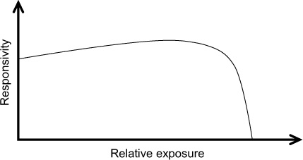
Figure 9.16 A generalized responsivity curve for a CCD or CMOS device.
As discussed in Chapter 2, a lens has a diffraction limit associated with it. So whilst reducing pixel size may aid resolution, setting it below this will not add any information to the image. It may be argued that there are some benefits using this method to reduce aliasing, though this approach could be considered expensive when compared to the alternatives, such as adding an anti-aliasing filter. For information on aliasing, see Chapter 7. Information on resolution may be found in Chapters 7 and 24.
Fill factor, the ratio of the light-collecting portion to the total size of the pixel, affects relative sensor sensitivity, as described previously. The source of this is readily apparent for interline CCDs and CMOS sensors; however, further electronics placed on the sensor surfaces can reduce this further. When a full well saturates, electrons are split from the saturated pixel to surrounding areas, causing corruption of those signals, known as blooming. To overcome this problem an antibloom drain is added to each pixel, dumping excess charge for highly illuminated areas. Though many different types exist, commonly a lateral overflow drain may be constructed adjacent to the photosite. This is essentially a reverse-biased diode that can draw off excess charge above a chosen level. These structures, however, are not sensitive to light and effectively reduce the fill factor.
Microlens arrays
Microlens arrays are added as a layer to the upper surface of the sensor to increase the effective fill factor of the pixel. A microlens, as the name implies, is a tiny lens formed to focus light into the pixel (Figure 9.17a). These arrays can increase the fill factors of some devices by 30–70%. The placement of microlenses has to take into account the variation in the chief ray angle (CRA) of the light hitting the pixel. Telecentric lenses are designed such that the light strikes the sensor orthogonally at all positions on the sensor, allowing it to be focused on to the correct pixel (Figure 9.17a). Most lenses, however, are not telecentric and the CRA varies with position in the field of view. This variation can cause the microlens to focus the light on to the adjacent pixel, causing colour shifts or optical crosstalk (Figure 9.17b). To overcome this problem, the lens must be designed such that its CRA, with respect to field of view, matches that specified by the sensor manufacturer for the particular sensor (Figure 9.17c).
Sensitivity
The fundamental spectral sensitivity of CCD and CMOS sensors is determined to a large extent by the silicon itself, modified by interference effects within the thin overlying layers forming part of the chip construction. The spectral sensitivity of a typical monochrome sensor is shown in Figure 9.18, from which it is seen that there is rather a low blue sensitivity and considerable sensitivity extending into the near-infrared region. In most sensors the infrared sensitivity is restricted by an infrared reflection or absorption filter on the face of the sensor, but in special purpose cameras a separate filter may be attached to the camera lens.
The use of a thin-film reflective infrared filter can introduce artefacts into colour images as the cut-off wavelength of the filter depends upon the angle of the arriving light. Towards the edge of the field of view where the CRA of the lens is greater, the filter cut-off is shifted towards the blue wavelengths, effectively cutting out more red light than at the centre of the field of view. This, in turn, causes a drop in red sensitivity towards the edge of the field of view of the sensor and a shift in the colour balance. Known as lens shading, algorithms in the image-processing pipeline can correct for this colour artefact by digitally amplifying those parts of the image where the red signal falls off.
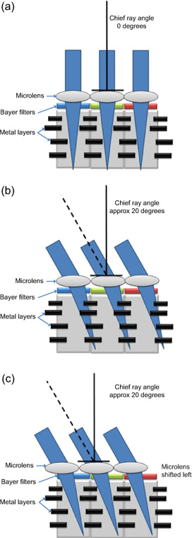
Figure 9.17 (a) If the CRA of the light striking the sensor is 0° the microlens will focus it into the sensitive region of the pixel. (b) The CRA varies with position in the field of view, causing the microlens to focus the light on to the adjacent pixel, creating colour shifts or optical crosstalk. (c) Shifting the microlenses may overcome this problem.
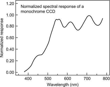
Figure 9.18 Spectral sensitivity of a typical monochrome silicon-based CCD or CMOS device.
Sensitivity for an image sensor can usefully be expressed as the ratio of incident photons to detected photons with respect to wavelength, or quantum efficiency (QE) as it is known. This topic is covered in more detail in Chapter 24. Responsivity, mentioned previously, is also covered in Chapter 24.
Alternatively, photometric units may be used to relate incident light to a ‘standard observer’ given a global figure of sensitivity. Calculating the number of lux necessary for the sensor to produce a signal that is discernible above the noise floor of the device is possible by relating the image illuminance necessary to produce the desired signal-to-noise ratio to the scene illuminance, presented in Chapter 24.
Spectral sensitivities for CCD and CMOS sensors are generally lower than those for bare silicon because of the effect of the polysilicon surface components. The polysilicon structure becomes less transparent at approximately 400 nm, attenuating blue light. A further problem is that the depth of penetration of the light is related to the wavelength, with red light travelling further into the photodiode than the blue. If the light does not reach the depletion region an electron–hole pair will not be generated and the quanta will not be detected (Figure 9.19). Due to the combination of these effects, CCD and CMOS sensors generally have lower sensitivity in the blue region of the spectrum. If a red quantum of light travels through the depletion region it will also not be detected and this is potentially a problem as the size of pixels falls and the corresponding size of the depletion region shrinks.
A typical sensor will have a DQE of approximately 30–40% (Chapter 24). By focusing an image on the back of the sensor and acid etching superfluous silicon substrate away, it is possible to increase the DQE of CCDs to beyond 80%. In addition, light does not have to traverse the polysilicon layers as above. So-called back thinning, until recently, has resulted in expensive delicate sensors suitable only for controlled environments where sensitivity is paramount. Modern manufacturing development, however, has resulted in a number of manufacturers pursuing back-side illumination (BSI) technology for the commercial market. DQE may also be increased by the use of anti-reflection coatings and the application of fluorescent dyes which absorb in the UV region of the spectrum and emit in the greeneblue.
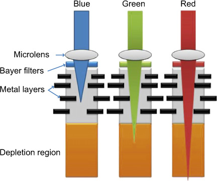
Figure 9.19 A representation of wavelength penetration in silicon devices.
Exposure control
Reduction of the effects of overexposure may be achieved in sensors by the use of electronic shutters. An electronic shutter can drain the charge from a pixel for a specific period of time and using this technique effective exposures down to 1 ms are readily achieved. The advantage of this technique is that a constant frame rate can be maintained despite varying levels of illumination and lack of mechanical shutter.
CMOS sensors more typically use rolling shutters. A rolling shutter uses pointers to enable the exposure of one portion of the sensor whilst reading out another. These pointers ‘roll’ throughout the lines on each frame, indicating when to read out, reset and expose. Whilst the technique increases the duty cycle of the sensor to near maximum, artefacts can be introduced into images if the camera or subject moves. This is because each part of the frame is exposed at a slightly different time (Figure 9.20). By extending or decreasing the time between the pointers the exposure time may be changed.
Extended shuttering allows capturing of scenes with large dynamic ranges. This may be thought of as the mathematical combination of different exposures made at different shutter speeds. By making successively shorter exposures, it is possible to capture very bright detail without saturation of the pixel. Using this technique, it is possible to record scenes with in excess of 90 dB dynamic range.
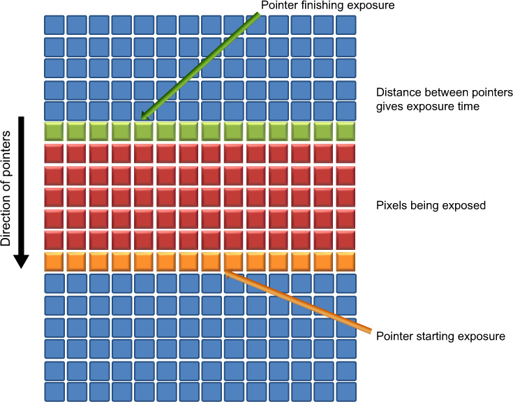
Figure 9.20 Rolling shutters as used in CMOS devices.
ISO settings in digital cameras essentially allow the user to trade noise for sensitivity. By increasing the ISO sensitivity, the camera shortens the exposure time and compensates this by increasing the levels of analogue and digital gain applied to the image. This increases the noise levels in the image.
Sensor imperfections
All sensors exhibit blemishes and manufacturers will generally set a threshold on each type of defect, above which it is discarded. The number of blemishes is proportional to the area of the sensor silicon and thus the manufacturing of devices is subject to a square law. In order to double the resolution of a device for a fixed pixel size, the area of silicon occupied quadruples. The likelihood of a sensor being discarded increases and the number of sensors per wafer falls. Hence to purchase a device with double the resolution the price is likely to more than double.
Dark pixels are those that have a lower response than the majority of those about them. They can be corrected for by a number of methods, including interpolation of surrounding values or by taking a flat-field reference image. Hot pixels generally saturate easily and generate a large amount of thermal noise (see Chapter 24). Again, these may be corrected using interpolation or a flat-field image. A flat-field image may be created by imaging a uniform source of light. From this the relative gains of each pixel may be determined and accounted for in the final image. Columns and rows may be affected in a similar manner depending upon the architecture of the device. Generally these effects are more serious and difficult to correct for. In the case of CCDs, pixels can act as traps or inefficient charge transfer sites. The image can therefore be smeared and affected throughout a column where these occur. Most CCDs and CMOS devices include defect correction in their image-processing pipeline and a user is unlikely to be aware of defects in the sensor. It is possible to buy sensors that have been sorted with respect to the numbers of defects exhibited. These generally cost disproportionately more and are primarily useful for scientific applications.
Generating colour
So far we have only considered arrays that respond to light intensity and in order to generate colour a number of methods are used. Colour is examined extensively in Chapters 5 and 23, and therefore only the physical aspects of generating colour are looked at here. Colour recording methods in digital cameras are also discussed in Chapter 14. One method is to successively record each image through red, green and blue filters and to additively record colour. Known as sequential colour, this method may be used for scanning colour originals and in some studio cameras where only static subjects are recorded as the time needed to change filters is generally large when compared to other methods. An advantage is that a larger number of filters may be used, giving very good colour fidelity. In addition, aliasing and demosaicing artefacts associated with the use of a Bayer array are avoided. This type of technique is advantageous for recording artwork where quality is paramount.
A second and by far the most predominant method used in consumer cameras today is to place a colour filter array (CFA) over the CCD. Although many configurations of the CFA have been developed (see Chapter 14), the most common is the Bayer pattern (Figure 9.21). There are generally twice as many green pixels present in a CFA array as this most closely corresponds to the peak sensitivity of the eye and the luminance component of images as perceived by humans. It is important to note that CFAs reduce the effective resolution of the camera sensor, since data has to be interpolated to provide the missing information at each pixel. If a red area is being recorded, it can be seen from Figure 9.21 that there will be pixels that will not have been activated. As the sampling pitch of each colour channel is different from that of a monochrome sensor, further artefacts may be introduced and readers are referred to the generation of aliasing artefacts or moiré patterns (see Chapters 7 and 19).
The third method involves the use of a beamsplitter to divide the input into three separate channels which separately record red, green and blue signals (or other appropriate combinations) on three CCD detectors. Whilst this is an expensive solution to the recording of colour, it allows higher resolution recording than is possible using CFAs.
A more recent technique has been developed by Foveon Inc., and exploits the wavelength-dependent penetration of light into silicon. It employs three vertically stacked photodiodes for each pixel and detects blue, green and red light with each. As it does not require interpolation, colour artefacts are reduced when compared with the use of a CFA array.
It is worth noting with all colour systems that the amount of light used for a particular colour channel is approximately a third of that for a monochrome camera and the light is necessarily filtered in order to be able to detect the relative colour components. This generally results in colour systems having lower effective sensitivities than their monochrome counterparts. Therefore, it is common to see monochrome sensors used for very-high-speed applications or those where the reduction of noise is critical.
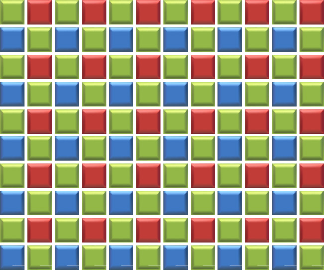
Figure 9.21 The Bayer CFA pattern.
As mentioned previously, CCD and CMOS sensors have a highly linear response. The eye, however, has a logarithmic response. This needs to be taken into account when generating images for viewing to achieve acceptable tone reproduction. Therefore, in addition to colour interpolation and correction via a colour correction matrix (CCM), the signal will also be gamma corrected as detailed in Chapter 21.
BIBLIOGRAPHY
Blouke, M.M., Sampat, N., Canosa, J., 2002. Sensors and camera systems for scientific, industrial, and digital photography applications II. Proceedings of SPIE. SPIE Optical Engineering Press, Bellingham, WA, USA.
Castleman, K.R., 1996. Digital Image Processing. Prentice-Hall, Englewood Cliffs, NJ, USA.
Dainty, J.C., Shaw, R., 1974. Image Science. Academic Press, New York, USA.
Gonzalez, R.C., Woods, R.E., 2007. Digital Image Processing, third ed. Addison-Wesley, Reading, MA, USA.
Gonzalez, R.C., Woods, R.E., Eddins, L.C., 2003. Digital Image Processing Using MATLAB®. Prentice-Hall, Englewood Cliffs, NJ, USA.
Holst, G.C., 1998. CCD Arrays, Cameras and Displays, second ed. SPIE Optical Engineering Press, Bellingham, WA, USA.
Jacobson, R.E., Ray, S.F., Attridge, G.G., Axford, N.R., 2000. The Manual of Photography, ninth ed. Focal Press, Oxford, UK.
Nakamura, J. (Ed.), 2006. Image Sensors and Signal Processing for Digital Still Cameras. CRC Press, Boca Raton, FL, USA.
Proudfoot, C.N. (Ed.), 1997. Handbook of Photographic Science and Engineering, second ed. IS&T, Springfield, VA, USA.
