5
Current FPGA Technologies
5.1 Introduction
By describing the details of the various technologies in the previous chapter, it becomes clear that the choice of the specific technology, and the resulting design approach implied by the technology, indicates the level of performance that will be able to be achieved for the specific DSP system under consideration. For example, the use of simple DSP microcontrollers implies a DSP system with relatively low performance requirements, and indicates that the user needs to produce C or C++ code as a source for its implementation. However, it is possible that the user can employ Matlab® or Labview as not only the initial design environment to scope the requirements such as wordlength or number representation for the system, but also to use the design approach and its available software routines, to produce the actual DSP source code for the microcontroller. Whilst it could be argued that the quality of the code produced by such approaches can be inefficient, it is quite possible that it is sufficient to meet the performance requirements of the applications, whilst still using a practical, i.e. low-cost, microcontroller, thus, meeting cost requirements as well, by reducing design time.
This design approach can be applied for the full range of ‘processor’ style platforms, but it may be required that dedicated handcrafted C code is produced, to achieve the necessary performance. This is probably particularly relevant in applications where performance requirements are tight (and cannot be met by the computational complexity of the platform), or the specific structure possesses dedicated functionality not well supported within the high-level tool environment; this is typically the case for the newer reconfigurable or dedicated processors, such as the Storm Stream Processor. In these cases, it is clear that the platform has been chosen as it offers some superior performance in terms of an area–speed–power metric; the attraction of the platforms could be in the form of specific features such as multiple MAC units of some commercial DSP platforms or, the dedicated processing functionality of the specialized DSP platform such as the data parallel unit of the Storm Stream Processor. In these cases, the user is having to compromise the ease of design, in order to avail of the specific architectural feature offered by the technology.
This notion is taken to extreme in the SoC concept where the user is now faced with creating the circuit architecture to best match the performance requirements of the specific system. The user can now create the system requirements to ultimately match the DSP systems requirements. However, this ideal notion is tampered with the practical limitations of being able to create this ultimate architecture, and hence, design approaches which either involve a specific, existing architectural style, or which utilize a range of existing building blocks, tend to dominate. This suggests an SoC implementation style, where a limited range of functionality will be employed to create systems within a reasonable time.
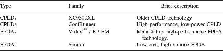
As Section 4.8 indicated, this is effectively what an FPGA platform offers; FPGAs have emerged from being a ‘glue logic’ platform, to become a collection of system components with which the user can create a DSP system. The purpose of this chapter is to give a reasonably detailed description of the current FPGA technologies, with a focus on how they can be used in creating DSP systems. The complete detail is given in the various data sheets available from the variety of companies who sell the technology, such as Xilinx, Altera, Atmel, Lattice and Atmel; however the chapter acts to stress the important features and highlights aspects that are important for DSP implementation. Whilst quite a number of different technologies are available from each company, the focus has been to concentrate of the latest commercial offering such as the Stratix® III family from Altera and the Virtex™-5 FPGA family from Xilinx. In addition, technology that is particularly different from other offerings is also described, such as the ProASICPLUS FPGA technology from Actel which is based on flash technology and the ispXPLD™ 5000MX family from Lattice which extends the CPLD concept (as compared to the LUT-based approach).
The chapter starts with a brief historical perspective of FPGAs in Section 5.2, describing how they have emerged from being a fine-grained technology to a technology with complex system blocks. Section 5.3 describes the Altera FPGA family, concentrating specifically on their Stratix® III FPGA family, as it represents the most powerful FPGA family that the company offers. The MAX® 7000 FPGA technology is also briefly described as it represents the evolution of the PLD concept which was architecture on which Altera based their initial programmable hardware offerings. Section 5.4 then goes on to describe the FPGA technology offerings from Xilinx, specifically the Virtex™ FPGA family. Once again, we concentrate on the most recent FPGA version of this technology, namely the Virtex™-5 FPGA family. With both Altera and Xilinx, we have tried to concentrate on the aspects of the hardware that are very relevant to DSP systems, but also have made an attempt to highlight other aspects such as high speed I/O, clocking strategy and memory organization, as these are also very important in determining overall system performance.
There are a number of other technologies offered by Actel, Atmel and Lattice that offer specific features and are very relevant in certain markets. For example, Lattice offer the ispXPLD™ 5000MX family which offers a combination of E2PROM nonvolatile cells to store the device configuration and SRAM technology to provide the logic implementation; these are described in Section 5.5. Actel® offer a number of FPGA technologies based on flash and antifuse technologies. Initially, Actel were known for, and still offer, an antifuse technology, namely the Antifuse SX FPGA technology which is described in Section 5.6.1. In Section 5.6.2, the ProASICPLUS flash, FPGA technology is described. This approach allows the device to store its program and remove the need for a programming device as in SRAM-based technology. The company's most recent offering, the Fusion™ technology which represents the first mixed signal FPGA, is also covered. Finally, the Atmel® AT40K FPGA technology is described in Section 5.7, as though a little older, it offers a partially reconfigurable solution. In Section 5.8, some conclusions are given.
5.2 Toward FPGAs
In the 1970s, logic systems were created by building PCB boards comprising of TTL logic chips. However, one the limitations was that as the functions got larger, the size of the logic increased, but more importantly, the number of logic levels increased, thereby compromising the speed of the design. Typically, designers used logic minimization techniques such as those based on Karnaugh maps or Quine–McCluskey minimization, to create a sum of products expression which could be created by generating the product terms using AND gates and summing them using an OR gate.
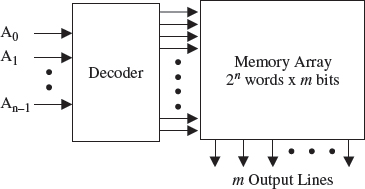
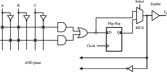
The concept of creating a structure to achieve implementation of this functionality, was captured in the programmable array logic (PAL) device, introduced by Monolithic Memories in 1978. The PAL comprised a programmable AND matrix connected to a fixed OR matrix which allowed sum of products structures to be implemented directly from the minimized expression. The concept of an AND and OR matrix became the key feature of a class of devices known as the programmable logic devices family; a brief classification is given in Table 5.1. As illustrated in Figure 5.1, a read only memory (ROM) possesses the same structure, only with a fixed AND plane (effectively a decode) and a programmable OR plane. In one sense, the structure can be viewed as providing the capability of storing four (in general 2n) of two- (or m-) bit words, as shown in Figure 5.2. The decoder, which is only required to reduce the number of pins coming into the memory, is used to decode the address input pins and a storage area or memory array is used to store the data. As the decoder generates the various address lines using AND gates and the outputs are summed using OR gates, this provides the AND–OR configuration needed for Boolean implementation. In general, a 2n by 1-bit ROM could implement any n-input Boolean function; a 4-input ROM or LUT thus became the core component of the very first FPGA, namely the Xilinx XC2000 FPGA. The 4-input LUT was small enough to achieve efficient utilization of the chip area, but large enough to implement a reasonable range of functions. If a greater number of inputs was required, this could be achieved by cascading or parallelizing the LUT inputs. This would result in a slower implementation, but it would provide a better utilization than with larger LUTs.
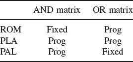
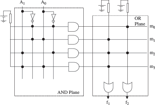
Figure 5.1 ROM detailed structure
The PLD structure had a number of advantages. It clearly matched the process of how the sum of products sum was created by the logic minimization techniques. The function could then be fitted into one PLD device, or if enough product terms were not available, could be fed back into a second PLD stage. Another major advantage was that the circuit delay is deterministic either comprising one level of logic level or two, etc. However, the real advantage came in the form of the programmability which reduced the risk in hardware PCB development, allowing possible errors to be fixed by adjusting the logic implementation of the PLD. However, as integration levels grew, the concept of using the PLD as a building block became an attractive FPGA proposition as illustrated by the early Altera offerings and indeed, by their current MAX 7000 device family. As mentioned earlier, Xilinx opted for the ROM or look up table (LUT) approach.
5.2.1 Early FPGA Architectures
The early FPGA offerings comprised a Manhattan style architecture where each individual cell comprised simple logic structures and cells were linked by programmable connections. Thus the FPGA could be viewed as comprising the following:
- programmable logic units that can be programmed to realize different digital functions
- programmable interconnect to allow different blocks to be connected together
- programmable I/O pins.
This was ideal for situations where FPGAs were viewed a glue logic as programmability was then the key to providing redundancy and protection against PCB board manufacture errors, and FPGA components could be used to provide programmable system interconnectivity; this might even provide a mechanism to correct faults caused by incorrect system design. However, technology evolution outlined by Moore's law, now provided scalability for the FPGA vendor. During the 1980s, this was exploited by FPGA vendors in scaling their technology in terms of number of programming blocks, numbers of levels of interconnectivity and number of I/Os. However, it was recognized that this approach had limited scope, as scaling meant that interconnect was becoming a major issue and technology evolution now raised the interesting possibility that dedicated hardware cells could be included, such as dedicated multipliers and more recently, processors. In addition, the system interconnectivity issue would also be alleviated by including dedicated interconnectivity in the form of SERDES and Rapid I/O.
Technology evolution has had a number of implications for FPGA technology:
Technology debate The considerable debate of which technology was effectively determined by Moore's law. In the early days, three different technologies emerged, namely conventional SRAM, antifuse and EPROM or E2PROM technologies. In the latter two cases, both technologies required special steps, either to create the antifuse links or to create the special transistors to provide the EPROM or E2PROM transistor. Technological advances favoured SRAM technology as it only required standard technology; this became particularly important for Altera and Xilinx, as the fabrication of FPGAs was being outsourced and meant that no specialist technology interaction with the fabrication companies was needed. Indeed, it is worth noticing that silicon manufacturers now see FPGA technologies as the most advanced technology to test their fabrication facilities.
Programmable resource functionality A number of different offerings again exist in terms of the basic logic block building resource used to construct systems. Companies such as Algotronix, Crosspoint and Plessey had offered FPGAs which were fine-grained with simple logic gates or multiplexers, being offered as the logic resources. With interconnect playing an increasing role in determining system performance, these devices were doomed, as described in Chapter 1. There also existed a number of options in the coarser-grained technologies, namely the PLDtype structure or the LUT. The PLD structure was related to logic implementation whereas the LUT was much more flexible and it was a concept understood by computer programmers and engineers. Examining the current FPGA offerings, it is clear to see that the LUT-based structure now dominates with the only recent evolution an increase in the size of the LUT from 4-input to 5/6-input in the Xilinx Virtex™-5 technology and to 6-input in the Altera Stratix® III family.
Change of FPGA market With the FPGAs growing in complexity, it now meant that the FPGA had gone from being primarily a glue logic component, to being a major component in a complex system with DSP being the target area of this book. However, it should still be observed that the FPGA is an important part of the telecommunications industry. This means that FPGA vendors have to compare their technology offerings in terms of new competitors, primarily DSP processor developers such as TI, Analog Devices and multi-core developers. Some of these technologies were presented in the previous chapter.
Tool flow Initially, FPGAs were not that complex, so up until the mid 1990s, it was usual that the designer would perform manual placement of designs. The first major tool development was automatic place and route tools which still plays a major role in the vendors’ tool flow. However, increasingly there is a well-recognized need for system-level design tools, to address latest design challenges. For this reason, FPGA vendors have been increasingly involved in developing systemlevel design tools such as the DSP and SOPC builder from Altera, and System Generator for DSP and AccelDSP™ from Xilinx in addition to system-level offerings from tools vendors. This is an increasing problematic issue as tools tend to lag well behind technology developments and is a major area of focus in this book.
It has now got to the stage that FPGAs represent system platforms. This is recognized by both major vendors who now describe their technology in these terms; in Xilinx's case, they describe their Virtex™ as a platform FPGA and with Altera, they describe their Stratix III as a high end being able to design entire systems-on-a-chip. Thus we have moved from the era of programmable cells connected by programmable interconnect as highlighted at the start if this section, to devices that are complex, programmable SoCs which comprise a number of key components, namely dedicated DSP processor blocks, soft and hard processor engines.
5.3 Altera FPGA Technologies
Altera is one of the two main FPGA companies and evolved their initial architectures, based on the PLD structure, described in the previous section. Its current FPGA portfolio is organized into several different technologies, as outlined in Table 5.2. Altera FPL families are organized into: configurable programmable logic devices (CPLDs) comprising the MAX® and MAX® II series families; low-cost FPGA families such as the Cyclone and Cyclone II families; high-density FPGA families such as the Stratix®, Stratix® II, Stratix® III and Stratix® GX families and; structured ASIC solutions HardCopy® and HardCopy® II families. The section will concentrate mostly on the Stratix® III family, as we are targeting DSP and particularly, high-performance DSP applications; however the MAX7000 series FPGA is also briefly reviewed as it is an obvious extension of the PLD concept.
Table 5.2 Altera's FPGA family range


Figure 5.3 Block diagram of Altera LE cell
The core block in the Altera FPGAs has been the logic element (LE) which is given in Figure 5.3. This is very similar to the Xilinx’s logic cell (LE) in their XC4000 and early Virtex™ FPGA families, although Xilinx have migrated recently to a 6-input LUT. The cell was built from the concept of meeting the criteria for implementing a purely combinational logic function (LUT table only), delay or shift function (flip-flop only) or sequential logic circuit (combinational logic feeding into flip-flops). Thus all configurations are provided along with various multiplexing and interconnection. The notion of choosing a 4-input LUT (rather than larger or smaller LUT) probably dates back to the work by Rose et αl. (1990) which showed that this size of LUT produced the best area efficiency for a number of different examples. Combinational logic implementations can then be constructed using series of these 4-input LUTs by using the programmable interconnect to link these 4-input LUTs together to build larger LUTs. The cell also provides a fast carry logic circuit for accelerating the implementation of adders using the approach, illustrated in Figure 3.3(b).
5.3.1 MAX® 7000 FPGA Technology
The basic PLD structure is given in Figure 5.4 where each of the PLD blocks are of the form given in detail in Figure 5.5. The framework provides a mechanism for connecting PLD blocks together via the programmable interconnect, in the same way that several PLD chips would have been connected to provide blocks of complex logic using commercial PLDs, with the added advantage that the PLD-based FPGA interconnect is programmable, the importance of which has already been highlighted on a number of occasions.
The MAX® and MAX® II series families from Altera (Altera Corp. 2000) are extensions of the basic concept of PLD technology. The MAX 7000 architecture is given in Figure 5.6 and consists of logic array blocks (LABs) which comprise 16-macrocell arrays, a programmable interconnect array (PIA) to allow connection of the blocks to each other and connection of various control inputs such as clock, reset etc., and I/O control blocks to allow internal interfacing to both the LABs and PIA. Four dedicated inputs allow high-speed, global control signals such as clock, reset and enable, to be fed into each macrocell and I/O pin. Each LAB is fed by 36 general logic signals from the PIA, global controls for use with the register part of the functionality and also direct connection to I/O pins to the registers in order to minimize delays for off-chip and on-chip communication.

Figure 5.4 Generalized PLD-based FPGA architecture
INPUT/GCLK1
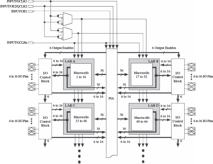
Figure 5.6 Altera MAX 7000E and MAX 7000S device block diagram. Reproduced by permission of Altera Corp.
The key computational part is the MAX 7000 macrocell given in Figure 5.7, which can be configured for either sequential or combinatorial logic operation. It consists of a logic array, a product-term select matrix and a programmable register. The logic array allows five product terms to be summed and product-term select matrix allows this to be used as the main (primary) output of the cell per macrocell, thereby providing a combinational output, or as part of a larger logic function, i.e. a secondary input to the register, allowing sequential logic circuits to be implemented. The flip-flop can be used as a delay, or part of a larger sequential circuit, and can be controlled in a number of ways in terms of reset or clock, using the various select functions. The cell also contains shareable expanders which allow inverted product terms to be fed back into the logic array, and parallel expanders to allow creation of larger fan-in logic functions by allowing inputs from other macrocells.
Logic is routed between LABs via the programmable interconnect array (PIA), which is a programmable path and allows any signal to connect to any destination on the device. The route is created by programming an E2PROM cell which controls one input of a 2-input AND gate thereby disabling or enabling the connection. One of the key advantages of the PLD is preserved in the PLD-based FPGA, namely the routing delays are fixed unlike other FPGA architectures described later, which are cumulative, variable, and path-dependent and can cause problems when achieving timing closure (timing closure is the process when all of the individual delays in the design have to meet the various timing constraints namely, critical path and edge to edge timing delays). Thus this makes the timing performance easier to predict. From a DSP perspective, these devices have limited usage as the main combinational blocks are for conventional logic implementations.
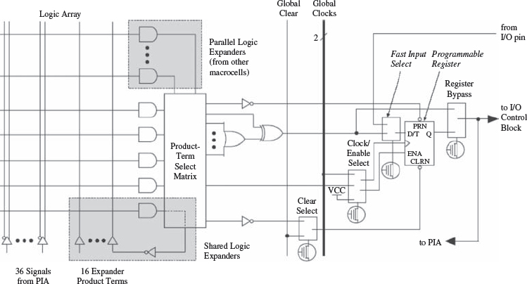
Figure 5.7 LAB block diagram. Reproduced by permission of Altera Corp.
5.3.2 Stratix® III FPGA Family
A number of variations exist for the Stratix® III FPGA family. The Stratix III E family would seem to be targeted toward DSP applications given the memory and multiplier rich for data-centric applications. The Stratix III E family offers a number of features useful for DSP applications, including: 48 000–338 000 equivalent LEs, up to 20 Mbits of memory and a number of high-speed DSP blocks that provide dedicated implementation of multipliers, multiply accumulate blocks and FIR filter functionality. In addition, the devices also provide adjustable voltage levels, a number of PLLs and various clocks. The floorplan of the Altera Stratix EP3SE50 is given in Figure 5.8.
Adaptive Logic Modules
In the Stratix III, the LE concept has been extended, leading to what Altera term an adaptive logic module or ALM, as shown in Figure 5.9. The ALM is based on 8-input LUT which can be fractured, allowing the original LE configuration of Figure 5.3; however, it also allows a number of other combinations, including not surprisingly, 7-input and 6-input LUTs, but also combinations of 5-input and 3-input, and even 5-input and 5-input, 4-input and 5-input, and 6-input and 6-input LUTs (as long as the total number of individual inputs does not exceed 8!). In addition, there are two dedicated adders and two registers. The 2:1 register-to-LUT ratio in ALMs ensures that the FPGA is not register-limited. The two adders can perform a 2-bit addition or a single ternary addition. The core concept of a LUT–multiplexer–register combination still remains, but just with a bigger LUT.
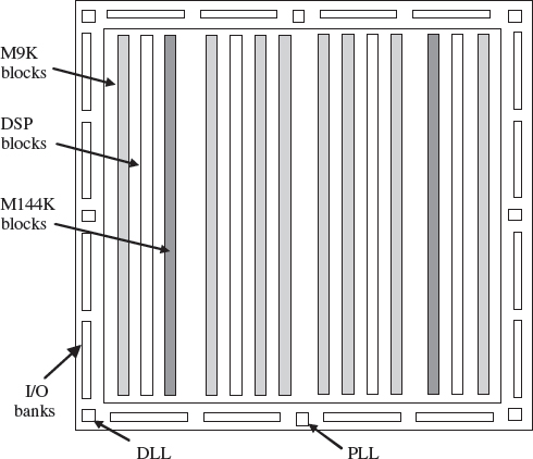
Figure 5.8 Altera Stratix EP3SE50 floorplan
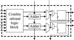
Figure 5.9 Altera ALM block diagram
Memory Organization
The Altera Stratix FPGA has a hierarchy of memory called TriMatrix memory, ranging from smaller, distributed memory blocks right through to larger memory blocks which provide a memory capacity of 17 Mbits, performing at rates of over 600 MHz. The types of memory are listed in Table 5.3. Three types are included and listed below:
MLAB blocks or memory LABs which are created from the ALMs and is a new derivative of the LAB. MLAB is a superset of the LAB and can give 640 bits of simple dual-port SRAM. As each ALM can be configured as either a 64×1or32× 2 block, the MLAB can be configured as a 64 × 10-bit or 32 × 20-bit simple dual-port SRAM block. MLAB and LAB blocks co-exist as pairs, allowing 50% of the LABs to be traded for MLABs. The MLABs would tend to be used as localized memory in DSP applications to store temporary and local data, thus giving high performance as a lot of the memory can be accessed in parallel.
Table 5.3 Stratix memory types and usage
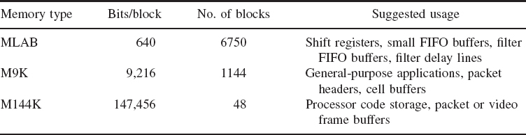
M9K blocks which are 9 kB block RAM allow storing of fairly large data. These are located as shown in Figure 5.8.
M144K blocks are larger, 144 kB of RAM, and from a DSP perspective for example, could be used in image processing applications to store images.
Each embedded memory block can be independently configured to be a single- or dual-port RAM, ROM, or shift register
DSP Processing Blocks
A key component of the Altera Stratix III FPGA, is the DSP function block; the largest Stratix device supports up to 112 such blocks, operating up to 550 MHz, thereby allowing huge performance capability for many DSP applications. The detailed block diagram for a half-DSP block is shown in Figure 5.10. The input wordlength to the input register block is 144 bits which is split into 8 of 18-bit words for the multiplier inputs shown as dataa and datab respectively; the output is 72 bits. The data is registered into and out of the DSP block, thereby avoiding any timing problems in meeting critical path delays, when the DSP block forms part of a larger system. In addition to these register inputs, the DSP blocks supports optional pipelining for higher speed, as indicated by the pipeline register bank in the figure. As will be seen in later chapters, the delays introduced by the pipeline stages, have to be taken into account in the development of the circuit architecture for the DSP function under consideration.
The first stage of the block comprises two dual multiplication/accumulation blocks which has been clearly developed to support specific DSP functions, namely: a 2-tap FIR filter configuration for each block, with the second stage adder/accumulator after the optional pipeline being used to sum the two 2-tap filters to give a four tap filter within the block; a part of a FFT bufferfly stage and; complex operations such as a complex multiplication, where the input stage ideally implements the complex multiplication of α + jb by c + jd given as (αc – bd) + j (αd + bc). The multipliers are 18-bit but can also function as two 9-bit multipliers. From the Altera literature (Altera Corp. 2007), it is also indicated that 9-bit, 12-bit, 18-bit and 36-bit word lengths are supported as well as signed and unsigned.
This multiply accumulate stage is then followed by an optional pipeline register bank and then the second stage adder/accumulator. Once again, the adder is configured to give maximum advantage to implement fast DSP systems, by providing a loop back from the output register bank allowing recurrence functions, commonly found in common in IIR filter implementations, to be computed. In addition, the DSP block provides the mechanism via the chainout adder, to add in the output from the DSP block above; this is possible as the DSP blocks are connected in columns as shown in Figure 5.8. This means it is now possible to implement a 4-tap filter by connecting two DSP blocks together in this way, and even much larger filters, with accordingly more DSP blocks.
Figure 5.10 Altera Stratix DSP block diagram (Altera Corp. 2007). Reproduced by permission of Altera Corp.
Rounding and saturation blocks are included after the second stage adder/accumulator and chainout adder blocks. The word growth is predictable in the first stage, but given that the output can be continually fed back via the loop back, it is essential to employ rounding and/or saturation to avoid overflow; likewise for the chainout adder when very larger filters are being created. The reasons for this have been highlighted in Chapter 4.
In summary, the DSP block can perform five basic DSP operations, as illustrated in Table 5.4 which is a summary of the information presented in the data sheet. This gives more detail on the arithmetic (signed/unsigned) and whether rounding can be applied. Two rounding modes are supported in namely round-to-nearest-integer which is normal rounding in DSP systems and round-to-nearest-even mode which as the name suggest rounds to nearest even number. Two saturation modes are supported, namely asymmetric and symmetric saturation. In 2's complement format, the maximum negative number that can be represented is –2n–1, i.e. –128 for 8-bit, while the maximum positive number is 2n–1 – 1, i.e. 127 for 8-bit. This is the range to which any number will be saturated in the asymmetric case, where the range is –2n + 1 i.e. –127 to 2n–1 – 1, i.e. 127 in the symmetrical case. There are 16 different cases for rounding and saturation in the 44-bit representation, thereby allowing a trade-off between accuracy and dynamic range, depending on the application.
Table 5.4 DSP block operation modes(Altera Corp. 2007)

Stratix Clock Networks and PLLs
Whilst it is important to understand the DSP blocks in detail for the FPGA technology under consideration, it is also important to have some appreciation of the clocking strategies and it can be critical in obtaining the required performance. The Stratix III devices have a number of dedicated global clock networks (GCLKs), regional clock networks (RCLKs), and periphery clock networks (PCLKs). These are organized into a hierarchical clock structure that provides up to 220 unique clock domains (16 GCLK + 88 RCLK + 116 PCLK). As the clock network can consume a considerable amount of power, the Quartus® II software compiler, automatically turns off clock networks not used in the design. The Stratix has up to 12 PLLs per device and up to 10 outputs per PLL, each of which can be programmed independently, allowing the creation of a customizable clock frequency, with no fixed relation to any other input or output clock.
In all, 16 GCLKs are provided which seem to be organized in an H clock tree network such as that shown in Figure 5.11. This provides an equal delay to each clock signal thereby balancing the skew. The GCLKs signals can drive functional blocks such as ALMs, DSP blocks, TriMatrix memory blocks and PLLs. Stratix III device I/O elements (IOEs) and internal logic can also drive GCLKs, to create internally generated global clocks and other high fan-out control signals such as globals resets or clock enables. The RCLK networks only pertain to the quadrant they drive into, and once again, can be used for globals resets or clock enables. Periphery clock (PCLK) networks are a collection of individual clock networks driven from the periphery of the Stratix III device.
Alternatively, the PLL can be used to synchronize the phase and frequency of an internal or external clock, fco to an input reference clock, fci. The basic diagram for a PLL of the type used in the Altera Stratix, is given in Figure 5.12. The voltage-controlled oscillator (VCO) generates a periodic output signal. If we assume that the oscillator starts at nearly the same frequency as the reference signal, then if the VCO falls behind that of the reference clock fci, this will be detected by a phase detector block called a phase-frequency detector (PFD). It will do this by generating an up (U) or down (D) signal that effectively determines whether the VCO needs to operate at a higher or lower frequency. These signals will then cause a circuit called a charge pump to change the control voltage, so that the VCO either speeds up or slows down. The low-pass filter sometimes called a loop filter, smooths out the abrupt control inputs from the charge pump, thereby preventing voltage overshoot and converts these U and D signals to a voltage that is used to bias the VCO via the bias generator, and thus determine how fast the VCO operates. A divider counter (÷N)in the feedback loop increases the VCO frequency, given as fco above the input reference frequency, meaning that the feedback clock to the PFD from the VCO is N times that of the input reference clock fci. Thus, the feedback clock applied to one input of the PFD is locked to the clock, fci that is applied to the other input of the PFD.
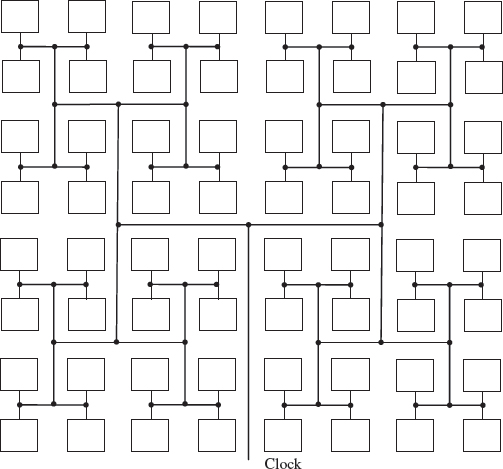
Figure 5.11 H tree buffer for clock
In the Altera Stratix FPGA, the VCO output from left/right PLLs in the FPGA die, feeds 7 postscale counters, whilst the corresponding VCO output from top/bottom PLLs can feed 10 post-scale counters. These counters then allow the generation of a number of harmonically related frequencies to be produced by the PLL.
Table 5.5 Typical memory interface speeds for Altera Stratix (Altera Corp. 2007)
I/O and External Memory Interfaces
The Stratix III FPGA produces a number of standard interfaces to each of the low-voltage CMOS and TTL standard programmable input and output pins. These pins are contained within a complex I/O element (IOE), located in I/O blocks around the Stratix device periphery; this contains bidirectional I/O buffers and I/O registers, allowing the pin to be configured for complete embedded bidirectional single or double data rate (DDR) transfer where both the rising and falling edges of the clock are used to accelerate data transfer. As indicated on Figure 5.8, there are up to four IOEs per row I/O block and four IOEs per column I/O block; the row IOEs drive the row, column, or direct link interconnects and the column IOEs, drive the column interconnects. A number of standard features are supported, including programmable input and output delay, slew rate, bus-hold and pull-up resistors, open-drain output as well as a number of on-chip series termination modes. This I/O configuration allows a 132 full duplex 1.25 Gbps true low-voltage differential signaling (LVDS) channels (132 Tx + 132 Rx) to be supported on the row I/O banks.
The I/O structure also provides support for high-performance external memory standards; DDR memory standards are supported such as DDR3, DDR2 and DDR SDRAM, QDRII+ and QDRII SRAM and RLDRAM II at frequencies of up to 400 MHz. A sample of some of the data rates for different speed grade technologies is listed in Table 5.5
Gigabit Transceivers
The Stratix® III device family offers a series of high-speed Gigagbit transceiver blocks, which allow data to be transferred at high speed, between different system devices in the DSP system, i.e. from chip to chip. The transceiver uses one pair of differential signals, i.e. a pair of signals which always carry opposite logical values, to transmit data and another set, to receive the data; hence the transmit and receive properties lead to the name transceiver. These transceivers operate at very high data rates, in the case of the Stratix® III device family at up to 1.25 Gbps and support a number of communication protocols such as Utopia and Rapid I/O™. These are explained below.
Conventional systems can be constructed by connecting systems devices using a hierarchy of buses; devices are thus placed at the appropriate level in the hierarchy, according to the performance level they require, i.e. low-performance devices placed at lower-performance buses, etc. A number of specific techniques have been introduced to achieve the performance requirements of individual connections, such as increasing bus frequency or width, splitting the transactions and allowing out-of-order completion. This required the development of individual system interfaces and complicated the design process. Over the past several years, with the development of the concept of the shared multi-drop bus that allows the full range of low/high bandwidth, high-speed communications has grown in interest. The Rapid I/O™ standard facilitates the operation of such a platform and effectively sits on top of the high speed gigagbit transceiver just described. In operation, a master or initiator processor generates a request transaction, which is transmitted to a target over the high-speed communications framework. The target then generates a response transaction back to the initiator to complete the operation. The Rapid I/O™ transactions are encapsulated in packets, which include all of the necessary bit fields to ensure reliable delivery to the targeted end point. Rapid I/O™ provides the same programming models, addressing mechanisms and transactions for both serial and parallel implementations, including basic memory mapped I/O transactions, port-based message passing and globally shared distributed memory with hardware-based coherency (Bouvier 2007). It can also manage any resulting errors that occur as each packet includes an end-to-end cyclic redundancy check (CRC). The adoption of Utopia and Rapid I/O™ thus reduces the design complexity by providing a standard interface for communications.
Device Security
Security is a major concern in FPGA technology as most of the major FPGA devices are based on SRAM technology; like standard memory, the contents can be easily read. Typically the designer will create a design using the commercial vendors' proprietary software, resulting in a configuration data file which programs the SRAM-based device. An EPROM can then be used to store the FPGA programming information, or more commonly it can be stored in system memory of an available microprocessor and loaded at power-up. Thus, the configuration information data can be captured, either from the EPROM or the FPGA SRAM configuration data locations in the FPGA which is a problem as it represents the designer's intellectual property.
A feature has thus been included in the Stratix III devices that allows the FPGA configuration bitstream to be encrypted using the industry standard, AES algorithm. The AES algorithm works on the principle of a security key stored in the Stratix III device, which is used to encrypt the configuration file. The design security feature is available when configuring Stratix III devices, using the fast, passive, parallel (FPP) configuration mode with an external host such as a microprocessor, or when using fast active serial or passive serial configuration schemes (Altera Corp. 2007). The design security feature is also available in remote update with fast active serial configuration mode.
5.3.3 Hardcopy® Structured ASIC Family
These devices are structured ASICs with pin-outs, densities, and architecture that complement Stratix® II devices. The main focus of the HardCopy® device is to strip the reprogrammable FPGA logic, routing, memory, and FPGA configuration-related logic and replace SRAM configuration resources by direct metal connections. Thus, it is envisaged that the designer would prototype the design using the Stratix® II FPGA family and then implement the volume product using HardCopy®.
The memory, clock networks and PLLs are identical in both devices as these are standard components, but the Stratix® II adaptive logic modules (ALMs) and dedicated DSP blocks are replaced by combinations of logic blocks, known as HCells. The Quartus II software used to implement the design, then uses the library of pre-characterized HCell macros to replace Stratix II ALM and DSP configurations before the design is transferred to the FPGA. This is achieved by having eight HCell macros which implement the eight supported modes of operation for the Stratix II DSP block for various forms of 9, 18 and 36-bit multiplication, multiply–accumulate and complex multiplication and addition.
The HardCopy® II memory blocks can also implement various types of memory, with or without parity, including true dual-port, simple dual-port, and single-port RAM, ROM, and FIFO buffers. HardCopy II devices support the same memory functions and features as Stratix II FPGAs, specifically the 4 k M4K RAM blocks and the 512-bit M-RAM blocks.
Of course, one the attractions of the structured ASICs compared with conventional SRAM-based FPGA implementations, is that they do not need to be programmed as the programmability has been effectively removed. Thus, some features need to be turned off such as the design security feature needed to encrypt the data stream and the configuration status pins. The HardCopy II structured ASIC follows the same principle of ASIC power-up except that is has an instant on time delay of 50 ms. During this time, all registers are reset; having resettable flip-flops is highly attractive feature as, for cost reasons, not all registers will be made to be resettable in ASIC implementations.
5.4 Xilinx FPGA Technologies
The first FPGA was the Xilinx XC2000 family developed in 1982. The basic concept was to have programmable cells, connected to programmable fabric which in turn were fed by programmable I/O as illustrated by Figure 5.13. This differentiated Xilinx FPGAs from the early Altera devices which were PLD-based; thus the Altera FPGAs did not possess the same high levels of programmable interconnect. The architecture comprised cells called logic cells or LCs which had functionality very similar to the Altera LE given earlier in Figure 5.3. The interconnect was programmable and was based on the 6-transistor SRAM cell given in Figure 5.14. By locating the cell at interconnections, it could then provide flexible routing by allowing horizontal-to-horizontal, vertical-to-vertical, verticalto-horizontal and horizontal-to-vertical routing, to be achieved. The I/O cell had a number of configurations that allowed pins to be configured as input, output and bidirectional, with a number of interface modes.
Figure 5.13 Early Xilinx FPGA architecture

Figure 5.14 Xilinx FPGA SRAM interconnect
Figure 5.15 Adder implementation on Xilinx Virtex™ FPGA slice
At this stage, FPGAs were viewed as glue logic devices with Moore's law providing a continual expansion in terms of logic density and speed. The device architecture continued largely unchanged from the XC2000 right up to the XC4000; for example, the same LUT table size was used. The main evolution was the inclusion of the fast adder where manufacturers observed that, by including an additional multiplexer in the LE cell, a fast adder implementation could be achieved by mapping some of the logic into the fast carry adder logic, and some into the LUT. The principle is illustrated for the Virtex™ FPGA device in Figure 5.15. At this stage, the device was still being considered as glue logic for larger systems, but the addition of the fast adder logic started to open up the possibility of implementing a limited range of DSP systems, particularly those where multiplicative properties were required, but which did not require the full range of multiplicands. This formed the basis for a lot of early FPGA-based DSP implementation techniques which are described in Chapter 6.
At that time, a lot of FPGA products manufacturers faded away and there began a period defined as accumulation (see Table 1.1) where FPGAs started to accumulate more complex components, starting with on-board dedicated multipliers, which appeared in the first Xilinx Virtex™ FPGA family (Figure 5.16), Power-PC blocks and gigabit transceivers with the Xilinx Virtex™-II pro and Ethernet MAC with the Virtex™-4. As with the Altera technology, it can be seen from Figure 5.16, that the Xilinx FPGA was now becoming increasingly like a SoC with the main aim of the programmability to allow the connection together of complex processing blocks with the LCs used to implement basic logic functionality. The fabric now comprised the standard series of LCs, allowing functions to be connected as before, but now complex processing blocks such as 18-bit multipliers and PowerPC processors (Figure 5.17), were becoming commonplace. The concept of platform FPGA was now being used to describe recent FPGA devices to reflect this trend. The full current FPGA family available from Xilinx is given in Table 5.6.
5.4.1 Xilinx Virtex™-5 FPGA Technologies
The text concentrates on the latest Virtex™ FPGA, namely the Virtex™-5 family on the basis that it represents a more evolved member of the FPGA family. Description of the CPLD family is not included on the basis that details are included on the Xilinx web pages. The Virtex™-5 comes in a variety of flavours, namely the LX which has been optimized for high-performance logic, the LXT which has been optimized for high-performance logic with low-power serial connectivity, and the SXT which has been optimized for DSP and memory-intensive applications with low-power serial connectivity. The Xilinx Virtex™-5 family has a two speed-grade performance gain and is able to be clocked at 550 MHz. It has a number of on-board IP blocks and a number of DSP48E slices which give a maximum of 352 GMACS performance. It also provides up to 600 pins, giving an I/O of 1.25 Gbps LVDS and, if required, RocketIO GTP transceivers which deliver between 100 Mbps and 3.2 Gbps of serial connectivity. It also includes hardened PCI Express endpoint blocks and Tri-mode Ethernet MACs.
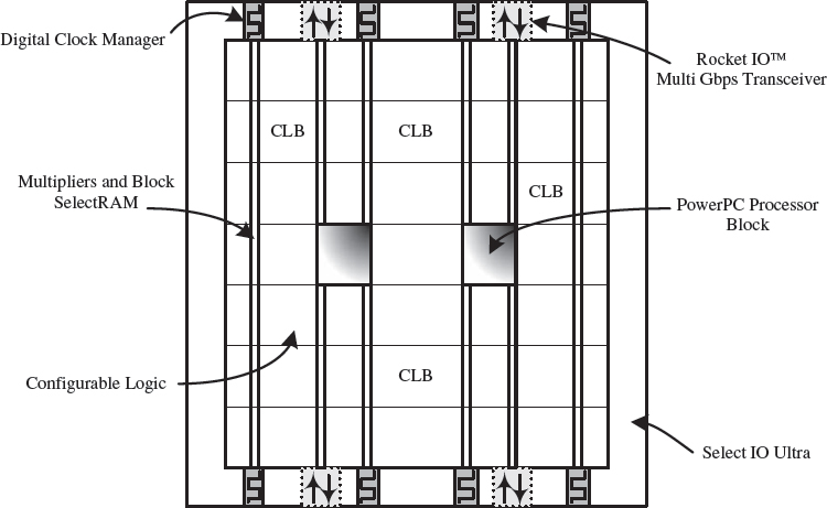
Figure 5.16 Virtex™-II Pro FPGA architecture overview
Table 5.6 Xilinx's FPGA family range
Virtex™-5 Configurable Logic Block
The logic implementation in the Xilinx device is contained within configurable logic blocks or CLBs. Each CLB is connected to a switch matrix for access to the general routing matrix as shown in Figure 5.18 and contains a pair of slices which are organized into columns, each with an independent carry chain. For each CLB, slices in the bottom of the CLB are labelled as SLICE(0), and slices in the top of the CLB, are labelled as SLICE(1) and so on. Every slice contains four logic-function generators (or LUTs), four storage elements, wide-function multiplexers, and carry logic and so can be considered to contain four of the logic cell logic as given in Figure 5.19. In addition to this, some slices, called SLICEM, support two additional functions: storing data using distributed RAM and shifting data with 32-bit registers.

Figure 5.17 PowerPC processor block architecture
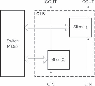
Figure 5.18 Arrangement of slices within the CLB
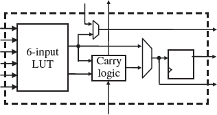
Figure 5.19 Logic cell functionality within a slice
The basic logic cell configuration is similar to the Altera LE given of Figure 5.3. It comprises a logic resource in this case, a 6-input LUT connected to a single flip-flop, via a number of multiplexers, together with a circuit for performing fast addition. As with the Altera LE element, the basic logic cell has been designed to cope with the implementation of combinational and sequential logic implementations, along with some simple DSP circuits that use an adder. The basic combination of LUT plus register has stayed with the Xilinx architecture, and has now been extended from a 4-input LUT in the Xilinx XC4000 series and Virtex™-5 series FPGA family to a 6-input LUT; this is a reflection of improving technology as governed by Moore's law. It is now argued in Xilinx Inc. (2007a) that a 6-input rather than a 4-input LUT which went all the way back to the study by Rose et αl. (1990), now provides a better return on silicon area utilization for the critical path needed within the design. The combination of LUTs, flip-flops (FFs), and special functions such as carry chains and dedicated multiplexers, together with the ways by which these elements are connected, has been termed ExpressFabric technology.
The CLB can implement the following: a pure logic function by using the 6-input LUT logic and using the multiplexers to bypass the register; a single register using the multiplexers to feed data directly into and out of the register; and sequential logic circuits using the LUTs feeding into the registers. Scope is also provided to create larger combinational and sequential circuits, using the multiplexers to create large LUTs and registers. One special feature of the 6-input LUT is that it has two outputs. This allow the LUT to implement two arbitrarily defined, five-input Boolean functions, as long as these two functions share common inputs (see Figure 5.20). This is an attempt to provide better utilization of the LUT resource when the number of inputs is smaller than six. This concept also allows the logic cell to implement a full adder, as shown in Figure 5.15 whilst at the same time, using the additional inputs and outputs to realize a 4-input LUT for some other function. This provides better utilization of the hardware in many DSP applications, where otherwise LUTs would be wasted to just provide a single gate implementation for a adder.
As with the Altera technology, the register resource is also very flexible, allowing a wide range of storage possibilities ranging from edge-triggered D-type flip-flops to level-sensitive latches, all with a variety of synchronous and asynchronous inputs for clocks, clock enables, set/reset. The D input can be driven directly from a number of sources, including the LUT output, other D-type flip-flops and external inputs.
One of the advantages of the larger LUT in the Xilinx Virtex™-5 device is that it provides larger distributed RAM blocks and SRL chains. A sample of the various distributed memory configurations is given in Table 5.7 which gives the number of LUTs needed to create the various memory configurations listed. The distributed RAM modules have synchronous write resources, and can be made to have a synchronous read by using the flip-flop of the same slice. By decreasing the clock-to-out delay, this will improve the critical path, but adds an additional clock cycle latency.
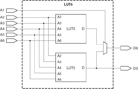
Figure 5.20 Arrangement of slices within the CLB
Table 5.7 Number of LUTs for various memory configurations
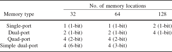
A number of memory configurations have been listed. For the single-port configuration, a common address port is used for synchronous writes and asynchronous reads. For the dual-port configuration, the distributed RAM has one port for synchronous writes and asynchronous reads, which is connected to one function generator and another port for asynchronous reads, which is connected to a second function generator. In simple dual-port configuration, there is no read from the write port. In the quad-port configurations, the concept is expanded by creating three ports for asynchronous reads, and three function generators plus one port for synchronous writes and asynchronous reads, giving a total of four functional generators.
The consideration of larger memory blocks is considered in the next section, but the combination of smaller distributed RAM, along with larger RAM blocks, provides the same memory hierarchy concept that was purported by the Altera FPGA, admittedly in different proportions. The LUT can also provide a ROM capability, and as Chapter 6 will illustrate, the development of programmable shift registers. The Virtex™-5 function generators and associated multiplexers some of which were highlighted in Figure 5.19, can implement one 4:1 multiplexers using one LUT, one 8:1 multiplexers using two LUTs etc.
Table 5.8 Virtex™-5 memory types and usage
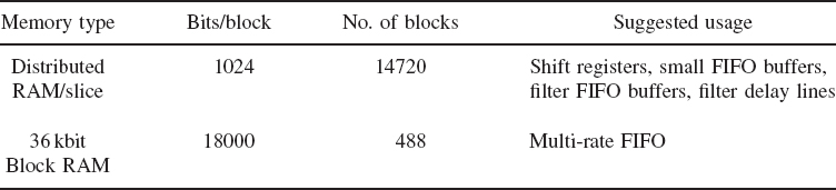
Memory Organization
In addition to distributed RAM, the Virtex™-5 device has a large number of 36kB block RAMs, each of which contain two independently controlled, 18 kB RAMs. The total memory configuration is given in Table 5.8. The 18 kB RAMs have been implemented in such a way, that the blocks can be configured to act as one 36 kB block RAM without the use of programmable interconnect. Block RAMs are placed in columns and can be cascaded to create deeper and wider RAM blocks. Each 18 kB block RAM, dual-port memory consists of an 18 kB storage area and two completely independent access ports along with other circuitry to allow the full expected RAM functionality to be achieved (See Figure 5.21). The full definition in terms of access pins is given below, and represents a standard RAM configuration.
A clock for each 18 kB block RAM which can be configured to have rising or falling edge. All input and output ports are referenced to the clock.
An enable signal to control the read, write, and set/reset functionality of the port with an inactive enable pin, implying that the memory keeps the previous state.
An additional enable signal called the byte-wide write enable signal which controls the writing and reading of the RAM in conjunction with the enable signal
The register enable pin which controls the optional output register.
The set/reset pin which forces the data output latches to contain a set value.
The address bus which selects the memory cells for read or write; its data bit width is decided by the size of RAM function chosen.
In latch mode, the read address is registered on the read port, and the stored data is loaded into the output latches after the RAM access time. When using the output register, the read operation will take one extra latency cycle. The write operation is also a single clock-edge operation with the write address being registered on the write port, and the data input is stored in memory. The additional circuitry highlighted in Figure 5.21, shows how inverted clock can be supported along with a registered output. The contents of the RAM can be initialized using the INIT parameter and can be indicated from the HDL source code.
The RAM provides a number of options for RAM configuration, some of which are listed in Table 5.9; the table shows how bit data width is traded off for memory depth, i.e. number of memory locations.
Dedicated logic has also been included in the block RAM enables, to allow the creation of synchronous or asynchronous FIFOs; these are important in some high-level design approaches, as will be seen later. This dedicated logic avoids use of the slower programmable CLB logic and routing resource, and generates the necessary hardware for the pointer write and read generation along with the setting of the various flags associated with FIFOs. A number of FIFO sizes can be inferred, including 8KX4, 4KX4, 4KX9, 2KX9, 2KX18, 1KX18, 1KX36, 512X36 and 512X72.
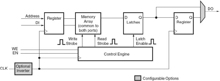
Figure 5.21 Block RAM logic diagram(Xilinx Inc. 2007b). Reproduced by permission of Xilinx Inc.
Table 5.9 Memory sizes for Xilinx Virtex™-5 block RAM
| Data width | Memory depth |
| 1 (cascade) | 32768 (65 536) |
| 2 | 16384 |
| 4 | 8192 |
| 9 | 4096 |
| 18 | 2048 |
| 36 | 1024 |
| 72 | 512 |
Virtex™-5 DSP Processing Resource
In addition to the scalable adders in the CLBs, the Virtex™-5 also provides a dedicated DSP processing block called DSP48E. The Virtex™-5 can have up to 640 DSP48E slices which are located at various positions in the FPGA, and supports many independent functions including multiply, MAC, multiply add, three-input add, barrel shifting, wide-bus multiplexing, magnitude comparator, bit-wise logic functions, pattern detect, and wide counter. The architecture also allows the multiple DSP48E slices to be connected together to form a wider range of DSP functions, such as DSP filters, correlators and frequency domain functions.
A simplified version of the DSP48E processing block is given in Figure 5.22. The basic architecture of the DSP48E block is a multiply–accumulate core, which is a very useful engine for many DSP computations. However, in addition to the basic MAC function, the DSP48E block also allows a number of other modes of operation, as summarized below:
- 25-bit x 18-bit multiplication which can be pipelined
- 96-bit accumulation or addition or subtracters (across two DSP48E slices)
Figure 5.22 DSP processing blocks called DSP48E(Xilinx Inc. 2007c). Reproduced by permission of Xilinx Inc.
- triple and limited quad addition/subtraction
- dedicated bitwise logic operations
- arithmetic support for overflow/underflow

Each DSP48E slice has a 25-bit X18-bit multiplier which is fed from two multiplexers; the multiplexers accept a 30-bit A input and a 18-bit B input either from the switching matrix or from the DSP48E directly below. These can be stored in registers (not shown in Figure 5.22) before being fed to the multiplier. Just before multiplication, the A signal is split and only 25 bits of the signal are fed to the multiplier. A fast multiplier technique is employed which produces an equivalent 43-bit two's complement result in the form of two partial products, which are then sign-extended to 48 bits in the X multiplexer and Y multiplexer respectively before being fed into three input adder/subtracter for final summation.
As illustrated in Chapter 4, many fast multipliers work on the concept of using fast carry-save adders to eventually produce a final sum and carry signals, and then using a fast carry ripple to perform the final addition. This final addition is costly, either in terms of speed or if a speed-up technique is employed, then area. By postponing the addition to the ALU stage, a two-stage addition can then be avoided for multiply–accumulation, by performing a three-stage addition to compute the final multiplication output and an addition for the accumulation input in one stage. Once again, for flexibility, the adder/subtracter unit has been extended to function as a arithmetic logic unit (ALU), thereby providing more functionality at little hardware overhead. As the final stage of the conventional multiplication is being performed in the second-stage adder, a three-input addition is required with the third input used to complete the MAC operation if required.
The multiplexers allow a number of additional levels of flexibility to be added. For example, the P input can be used to feed in an input either from another DSP48E block from below using the PCIN in the Z multiplexer or looped back from the current DSP48E block say, for example, if a recursion is being performed using the P input to the Z multiplexer. The multiplier can be bypassed if not required, by using the A:B input which is a concatenation of the two input signals A and B, 25-bit and 18-bit words respectively; this gives a 43-bit word size which is the same as the multiplier output. Provision to initialize the inputs to the ALU to all 0s or all 1s, is also provided. To increase the flexibility of the unit, the adder can also be split into several smaller adders, allowing two 24-bit additions or four 12-bit additions to be performed. This is known as the SIMD mode, as a single operation namely addition, is performed on multiple data, thus giving the SIMD operation. The DSP48E slice also provides a right-wire-shift by 17, allowing the partial product from one DSP48E slice to be shifted to the right and added to the next partial product, computed in an adjacent DSP48E slice. This functionality is useful, when the dedicated multipliers are used as building blocks, in constructing larger multipliers.
The diagram in Figure 5.22 is only basic, and does not indicate that other signals are also provided, in addition to the multiply or multiply–accumulate output, P. These include:
The cascadable A data port called ACOUT, which allows the A internal value to be fed directly to the output. Given that the A signal has been internally delayed, this would provide the delay chain for DSP functions e.g. a FIR filter.
Cascadable carryout (CARRYCASCOUT) and sign (MULTSIGNOUT) signals which are internal signals used to indicate the carryout and sign, when supporting 96-bit addition/subtraction across two DSP48E slices.
Up to four carry out signals (CARRYOUT) to support the SIMD mode of addition where up to four separate adders will need to generate carry out signals.
A pattern detector provides support for a number of numerical convergent rounding, overflow/underflow, block floating-point, and support for accumulator terminal count (counter auto reset) with pattern detector outputs (PATTERNDETECT and PATTERNBDETECT), to indicate if a pattern has been met and separate signals for overflow (OVERFLOW) and underflow (UNDERFLOW).
From a functional perspective, the synthesis tools will largely hide the detail of how the design functionality is mapped to the FPGA hardware, but it is important to understand that the level of functionality that is available as it determines the design approach the user will adopt. A number of detailed examples are listed in the relevant user guide (Xilinx Inc. 2007c), indicating how performance can be achieved.
Clock Networks and PLLs
The Xilinx Virtex™-5 FPGA family can provide a clock frequency of 550 MHz. The clock domains in the Virtex™-5 FPGA are organized into six clock management tiles or CMTs, each of which contain two digital clock managers (DCMs) and one PLL. In total, the FPGA has eighteen total clock generators.
A key feature of the Xilinx Virtex™-5 FPGA is the DCM, which provides a wide range of powerful clock management features including a delay-locked loop(DLL);thisacts toalignthe incoming clock to the produced clock as described earlier. It also allows a range of clock frequencies to be produced, including a doubled frequency a range of fractional clock frequencies specifically 1.5, 2, 2.5, 3, 3.5, 4, 4.5, 5, 5.5, 6, 6.5, 7, 7.5, 8, 9, 10, 11, 12, 13, 14, 15, or 16 of the input clock. Coarse (90°, 180° and 270°) fine-grained phase shifting and various types of fine-grained or fractional phase-shifting are supported.
The PLL's main purpose is to act as a frequency synthesizer and to remove jitter from either external or internal clocks, in conjunction with the DCMs. With regard to clock generation, the six PLL output counters are multiplexed into a single clock signal for use as a reference clock to the DCMs. Two output clocks from the PLL can drive the DCMs; for example, one could drive the first DCM while the other could drive the second DCM. Flexibility is provided to allow the output of each DCM output to be multiplexed into a single clock signal, for use as a reference clock to the PLL, but one DCM can be used as the reference clock to the PLL at any given time (Xilinx Inc. 2007c).
I/O and External Memory Interfaces
As with the Altera FPGA device, the Virtex™-5 FPGA supports a number of different I/O standard interfaces termed SelectIO™ drivers and receivers, allowing control of the output strength and slew rate and on-chip termination. As with the Altera FPGA, the I/Os are organized into a bank comprising 40 IOBs which covers a physical area that is 20 CLBs high, and is controlled by a single clock. The Virtex™-5 FPGA also includes digitally controlled impedance (DCI) technology, allowing the output impedance or input termination to be adjusted, and therefore, accurately match the characteristic impedance of the transmission line. The need to effectively terminate PCB trace signals, is becoming an increasing important issue in high-speed circuit implementation, and this approach purports to avoid the need to add termination resistors on the board. A number of standards are supported, including low-voltage transistor–transistor logic (LVTTL), low-voltage complementary metal oxide semiconductor (LVCMOS), peripheral component interface (PCI) including PCIX, PCI33, PCI66, and low-voltage differential signalling (LVDS), to name but a few.
Input serial-to-parallel converters (ISERDES) and output parallel-to-serial converters (OSERDES) are also supported. These allow very fast external I/O data rates such as SDR and DDR, to be fed into the internal FPGA logic which may be running an order of magnitude slower. This is essentially a serial-to-parallel converter with some additional hardware modules that allow reordering of the sequence of the parallel data stream going into the FPGA fabric, and circuitry to handle the strobe-to-FPGA clock domain crossover.
5.5 Lattice® FPGA Families
Lattice® offer a number of FPGA architectures, including the ispXPLD™ 5000MX family which extends the CPLD concept, the LatticeSC/M family which is a more of a standard FPGA with additional high-speed communications, memory and dedicated ASIC block implementation, and the Lattice ECP2/M family which is a low cost FPGA with a number of the features outlined in the LatticeSC/M family.
5.5.1 Lattice® ispXPLD 5000MX Family
The ispXPLD™ 5000MX family offers a combination of E2PROM nonvolatile cells which stores the device configuration, and SRAM technology to provide the logic implementation, giving a solution that provides logic availability at boot-up. It also includes flexible memory capability, supporting single- or dual-port SRAM, FIFO, and ternary content addressable memory (CAM) operation along with dedicated arithmetic functionality. However, the technology benefits from the main attraction of using the CPLD architecture to provide predictable deterministic timing. The architecture of ispXPLD 5000MX device (Figure 5.23), consists of units called multi-function blocks (MFBs) interconnected with a global routing pool which are connected via multi sharing arrays (MSAs) to the input and output pins. The MFB consists of a multi-function array and associated routing, which can cope with up to 68 inputs from the GRP and the four global clock and reset signals and produce outputs to the macrocells or elsewhere. The device allows cascading of adjacent MFBs to support wider operation. Each MFB can be configured in a number of modes, including logic and memory configurations e.g., single- and dual-port RAM, FIFO Mode and CAM.
This description concentrates on the LatticeSC/M FPGA (Lattice Semi. Inc. 2007), as it represents the high-performance FPGA family, with many of the features which appear on the lower cost Lattice ECP2/M families. The architecture of LatticeSC/M device is given in Figure 5.24. It comprises the standard programmable I/O block which is connected to rows of logic blocks organized as programmable functional units or PFUs. These PFUs comprise slices, each of which comprise two 4-input LUTs and two registers, along with carry propagate and carry generate signals which allow the creation of fast adder structures. As with other FPGA offerings, this functionality can be used to create combinational and sequential logic with the capability to scale LUT table sizes and register dimensions as required. As in the ispXPLD™ 5000MX family, the PFUs can also be configured to act as memory types. The largest device offers 115 k of LUTs.
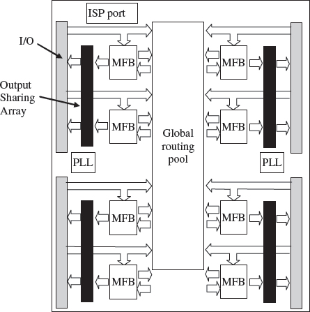
Figure 5.23 Lattice ispXPLD 5000MX family
In addition to the programmable logic, the device also incorporates up to 7.8 Mb of embedded block RAM, to match the 2 Mb of distributed RAM contained within the PFUs. These sysMEM EBRs as they are called, can be configured as RAM, ROM or FIFO, allowing a high level of programmability. In addition to the standard programmable I/O pins, high performance I/O is included in the form of dedicated SERDES and PCS hardware which provides 2Gbps I/O capability. This matches the concept of gathering large dedicated IP functionality on IP cores.
A feature that is different from offerings from Altera and Xilinx, is the structured ASIC capability as highlighted in Figure 5.25. This masked array for cost optimization or MACO block is a sea of 50 000 ASIC gates which has been created using a 90 nm CMOS process technology and optimized for speed, power dissipation, and area (Lattice Semi. Inc. 2006). The MACO block interfaces directly to the I/O and also to the FPGA fabric, thereby allowing dedicated fast low-power implementation for specialized hardware. In addition to the gates, each MACO block contains three 64× 40 asynchronous dual-port RAMs in addition to the RAM of the FPGA; the dual-port RAMs are co-located to the MACO block and can be accessed through the dedicated MACO interface block or MIB. By being located between the I/O pins and the on-board block RAM makes this ideal for implementing a number of fast, lower-power blocks such as dedicated or specialized memory interfaces.
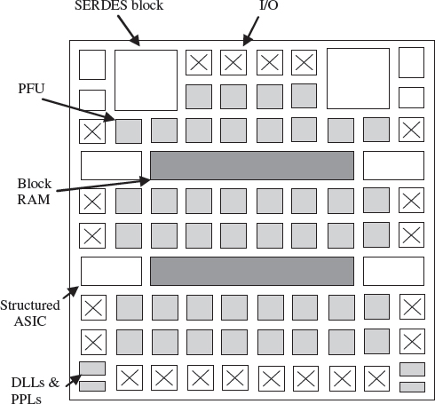
Figure 5.24 LatticeSC/M Family
5.6 Actel® FPGA Technologies
Actel® offers a number of FPGA technologies, based on flash and antifuse technologies. They have also recently launched a Fusion™ technology which represents the first mixed signal FPGA (Actel Corp. 2007a). It comprises A/D converters, embedded flash memory and as well as more conventional digital FPGA hardware in the form of D-type flip-flops and RAM. The flash technology is nonvolatile, meaning that the FPGA stores its design and is live at power-up, without the need to be programmed from a ROM or co-processor. The largest device has 1.5 M system gates with 270 kbits of dual-port SRAM, up to 8 Mbits of flash memory, 1 kbit of user flash ROM, and up to 278 user I/Os.
5.6.1 Actel® ProASICPLUS FPGA Technology
The ProASICPLUS FPGA technology is based on flash technology. It is similar to E2PROM technology in that it stores its charge and therefore allows the device to store its program. The FPGA technology is organized with an architecture comparable to gate arrays, as illustrated in Figure 5.25, and comprises a sea of tiles where each tile can be configured as a three-input logic function, or a D-type flip-flop. As the diagram shows, the architecture comprises a grid of tiles with a number of embedded two-port SRAM blocks, top and bottom which allow synchronous and asynchronous operation. The tiles consist of a number of multiplexers and logic gates, sufficient to allow the creation of a flip-flop with the necessary globally connected reset and clock signalling. The tiles connect to both the local and the longer line routing.
The tiles are connected by a hierarchy of routing that has four levels which are organized in terms of length; it would appear to have a similar organisation to the older Xilinx XC62000 FPGA technology which was a similarly fine-grained architecture. The next level of lines run one, two or four tiles. Both of these are accessible at the tile output. The next level of interconnect are long-line resources which span the length of the chip. The final level is global signals, which by definition have to be low-delay, as they will be used for global signals such as clock, reset and enable signals which would be used globally and would degrade the performance of the chip.
Figure 5.25 Actel® ProASICPLUS FPGA (Actel Corp. 2007b). Reproduced by permission of Actel Corp.
The device also incorporates two clock conditioning blocks which, like other FPGA devices, comprise PLLs and delay circuits for synchronizing the external clock as well as multiplier/dividers circuits along with necessary circuitry to connect to the global routing network. The device comes with four clock networks or global trees, specifically designed for distributing a low-latency, lowskew clock signal.
A key aspect of the implementation process with such a fine-grained technology, is the good placement of the design units into the hardware, as the limited routing organization can hamper design quality and utilization of the underlying hardware blocks. For this reason, the software allows the use of constraints to control the placement of the design. The concept of generating a circuit architecture to best match the FPGA resource requirements, is definitely needed, not only to achieve the necessary performance, but also to alleviate the software effort in achieving an efficient implementation. As with other FPGAs, a range of I/O blocks is available and boundary scan in the form of JTAG is provided for system text at the board level.
5.6.2 Actel® Antifuse SX FPGA Technology
In addition to flash memory devices, Actel also provide an antifuse technology which is once-only programmable. An antifuse is a two-terminal device with an unprogrammed state presenting a very high resistance between its terminals. Typically as shown in Figure 5.26, two conductors are separated by mostly insulator, but at certain points by amorphous or ‘programmable’ silicon. When a high voltage is applied across its terminals, the antifuse will ‘blow’ and create a low-resistance link (as opposed to an open circuit as in a fuse).
In the case of the Actel antifuse link shown in Figure 5.27, the connection is made up from a combination of amorphous silicon and dielectric material and has an ‘on’ state resistance of 25ω with a capacitance of 1.0 fF (Actel Corp. 2007c). The use of three-layer metal as shown in Figure 5.27 and the use of metal-to-metal antifuse results in better performance and smaller area. The metal-to-metal antifuse lowers the programmed resistances, thereby providing better speed, and the multiple metal layers now allows the placement of the antifuses above the logic, thereby avoiding routing channels. This provides better density of logic and lead to smaller devices with better, performance.
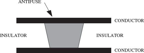
Figure 5.26 Basic antifuse link

Figure 5.27 Actel® ProASICPLUS FPGA(Actel Corp. 2007c). Reproduced by permission of Actel Corp.
The architecture comprises a sea of modules which like the ProASICPLUS FPGA technology, is fine-grained with two types of cells, namely a C-cell which is effectively a combinational cell comprising a series of multiplexers and logic gates, and an R-cell which is a register cell which comprises a D-type flip-flop with various multiplexing hardware, to allow various connections to the input, and to allow various clock signals to be used to clock the cell. Because of the programmability to configure the cell, the fabric is comprised of a variety of the different cell types, meaning that pre-defined mappings of the cells must be created, called clusters. The two types of superclusters are illustrated in Figure 5.28; the one supercluster comprises two C, R and C clusters and the other supercluster comprises a C, R and R cluster followed by a C, R and C cluster.
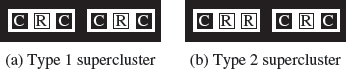
Figure 5.28 Cluster organization
In this structure, a number of different level of routing is given. The first type of routing comprises the DirectConnect which is a horizontal routing resource that connects from C-cell to its neighbouring R-cell in a cluster, and the FastConnect routing which provides vertical routing. Two globally orientated routing resources are also provided, known as segment routing and high-drive routing, which as the names suggest are for smaller routes, i.e. segments and more global routes. As with the ProASICPLUS FPGA technology, consideration has to be given to the careful placement of the cells in order to achieve efficient implementation, otherwise the disadvantage of the delays of programmable routes will have to be suffered.
Clock rates of 300 MHz are quoted in (Actel Corp. 2007c). In addition, it is also argued that security is a key feature of the technology, as it proves difficult to reverse engineer the device because it is hard to distinguish between the programmed and unprogrammed antifuses, and there is no configuration bitstream to intercept.
5.7 Atmel® FPGA Technologies
Atmel offer a range of FPGA technologies, ranging from the AT40K and AT40KAL series coprocessor FPGAs range which offer the concept of what is termed FreeRAM™ which can be used without infringing the available logic resource. Their FPGA technology can be used as an embedded core in the form of FPSLIC™ FPGA family, which provides from 5 k up to 50 k gates, up to 36 k of SRAM and a 25 MHz AVR MCU. The AT6000 series FPGAs are marketed as reconfigurable DSP co-processors, as they offer register counts of 1024 to 6400 registers, making them ideal for use as computing DSP functions that have been off-loaded into hardware. One of the key features of the AT6000, AT40K and AT40KAL FPGA families is that they offer reconfigurability, allowing part of the FPGA to be reprogrammed without loss of register data, whilst the remainder of the FPGA continues to operate without disruption. For this reason, the AT40K FPGA family are considered in a little more detail.
5.7.1 Atmel® AT40K FPGA Technologies
The AT40KAL is a SRAM-based FPGAs with distributed dual-port/single-port SRAM and eight global clocks with only one global reset. The family ranges in size from 5000 to 50 000 usable gates. The AT40KAL is a fine-grained FPGA architecture comprising simple cells organized into 4 × 4 grids, each of which are surrounded by repeater cells, as shown in Figure 5.29 (Atmel Corp. 2006). The repeaters regenerate the signals and allow connection of any bus to any other bus, on the same plane. Each repeater has connections to two adjacent local-bus segments, which provide localized connections in the four cells shown, and two express-bus segments for longer line connection which spans eight cells.
The core cell is very fine-grained, comprising two 3-input LUTs (8 × 1 ROM) which can be configured as a 4-input LUT, a D flip-flop, a 2-to-1 multiplexer and an AND gate for implementing multiplier arrays. As with the other FPGA technologies, the combination of LUT and D-type flip-flops allow a wide range of combinational and sequential logic to be implemented. There is a DSP mode, but it is basic, compared with other technologies, as it only allows the generation of an array multiplier using the cells, resulting in a relatively poor DSP performance compared with other FPGA technologies.

Figure 5.29 Atmel AT50K FPGA 4 × 4 cell
At the intersection of each repeater row and column, there is a 32 × 4 RAM block accessible by adjacent buses, which can be individually addressed through the provision of a series of local, and express horizontal and vertical buses. Reading and writing of the dual-port FreeRAM are independent of each other, and reading is completely asynchronous.
An interesting aspect of the Atmel® AT40K FPGA technology is the fact that it can be partially reconfigured, i.e. programmed, allowing the function of the design or part of the design to be changed whilst it is operating. This is worth examining in a little more detail.
5.7.2 Reconfiguration of the Atmel® AT40K FPGA Technologies
The AT40K FPGA technology has four basic configuration modes of operation (Atmel Corp. 2006). First, there is power-on reset when the device is first powered up which involves a complete reset of all of the internal configuration SRAM. Second, the same reset sequence can be invoked by the manual reset, via the reset pin. The third configuration mode is configuration download, where the FPGA's configuration SRAM is programmed using serial, or parallel data via its input pins. The fourth mode is when no configuration is active. The AT40K FPGA allows complete reconfigurability down to the byte level.
The CacheLogic® architecture lets users reconfigure part of the FPGA, while the rest of the FPGA continues to operate unaffected; this done using a windowing mechanism. This allows the user to load the SRAM memory map in smaller segments, allowing overwriting of portions of the configuration SRAM that is not being used, with new design information. In synchronous RAM mode, the device receives a 32- or 40-bit-wide bitstream composed of a 24-bit address and either an 8-bit-wide or 16-bit-wide dataword. Address, data and write enable are applied simultaneously at the rising edge of CCLK. In this mode, designed to interface to a generic IO port of a microprocessor, the FPGA configuration SRAM is seen as a simple memory-mapped address space. The user has full read and write access to the entire FPGA configuration SRAM. The overhead normally associated with bitstreams is eliminated, resulting in faster reconfiguration.
5.8 General Thoughts on FPGA Technologies
The chapter has covered a number of FPGA technologies from a variety of companies, but highlighting the two major vendors, namely Xilinx and Altera. The major drive in FPGA technology, has been a move from an FPGA being a fine-grained device where simple logic was implemented using LUTs and programmable interconnect, to one where it is a collection of heterogeneous complex units such as dedicated DSP blocks, high-speed communications blocks, soft and hard processor and of course, the previously mentioned LUTs.
This has had a number of implication for the design process. With earlier FPGAs, the target has been to develop an efficient implementation where utilization of FPGA hardware had been the main focus. This involved using, initially, schematic design capture packages and then more recently HDL-based tools, to achieve an efficient design implementation. Given that the focus was to achieve high utilization, considerable effort was expended to utilize the underlying LUTs. Thus, a number of circuit-level design techniques were developed to best use LUTs, and flip-flops for that matter, to achieve the implementation. These techniques are covered in more detail in Chapter 6 as it is important to understand the principles, even though a lot of this activity is carried in synthesis tools. For this reason, the design techniques are only briefly covered.
As complexity has grown with more recent FPGAs, the major challenge has been to create a circuit architectures at one level (see Chapter 8) and then system-level architectures at another level which is a major focus in Chapters 7, 9 and 11. There has been a major focus on generating circuit architectures that contain all of the FPGA specific details from a SFG representation of the DSP algorithm. Since the major performance gains of FPGAs in the area of DSP implementation, this involves exploiting concurrency in terms of parallelism and pipelining. The processes for achieving this are described in detail in Chapter 8; the higher-level tools flows are then described in the later chapters.
References
Actel Corp. (2007a) Fusion family of mixed-signal flash FPGAs with optional soft arm support. Web publication downloadable from www.actel.com.
Actel Corp. (2007b) Proasicplus flash family FPGAs. Web publication downloadable from www.actel.com.
Actel Corp. (2007c) Sx family FPGAs. Web publication downloadable from www.actel.com.
Altera Corp. (2000) Max ii device family data sheet. Web publication downloadable from http://www.altera.com.
Altera Corp. (2007) Stratix iii device handbook. Web publication downloadable from http://www.altera.com.
Atmel Corp. (2006) 5k–50k gates coprocessor FPGA with freeram. Web publication downloadable from http://www.atmel.com.
Bouvier D (2007) Rapidio: the interconnect architecture for high performance embedded systems. Web publication downloadable from http://www.techonline.com/.
Lattice Semi. Inc. (2006) Delivering FPGA-based pre-engineered IP using structured ASIC technology. Web publication downloadable from www.latticesemi.com.
Lattice Semi. Inc. (2007) Latticesc/m family data sheet. Web publication downloadable from www.latticesemi.com.
Rose J, Francis RJ, Lewis D and Chow P (1990) Architecture of field programmable gate arrays: the effect of logic block functionality on area efficiency. IEEE Journal of Solid State Circuits 25(5), 1217–1225.
Xilinx Inc. (2007a) Achieving higher system performance with the virtex-5 family of FPGAs. Web publication downloadable from www.xilinx.com/bvdocs/whitepapers/wp245.pdf.
Xilinx Inc. (2007b) Virtex-5 user guide. Web publication downloadable from www.xilinx.com.
Xilinx Inc. (2007c) Xilinx ug193 virtex-5 xtremedsp design considerations: User guide. Web publication downloadable from www.xilinx.com/bvdocs/userguides/ug193.pdf.