1
Introduction to Field-programmable Gate Arrays
1.1 Introduction
Electronics revolutionized the 20th century and continues to make an impact in the 21st century. The birth and subsequent growth of the computer industry, the creation of mobile telephony and the general digitization of television and radio services has largely been responsible for the recent growth. In the 1970s and 1980s, electronic systems were created by aggregating standard components such as microprocessors and memory chips with digital logic components, e.g. dedicated integrated circuits (ICs) along with dedicated input/output (I/O) components on printed circuit boards (PCBs). As levels of integration grew, manufacturing working PCBs became more complex, largely due to increased component complexity in terms of the increase in the number of transistors and I/O pins but also the development of multi-layer boards with up to as many as 20 separate layers. Thus, the probability of incorrectly connecting components also grew, particularly as the possibility of successfully designing and testing a working system before production was coming under increasingly limited time pressure.
The problem was becoming more intense due to the difficulty that system descriptions were evolving as boards were being developed. Pressure to develop systems to meet evolving standards, or that could change after the board construction due to system alterations or changes in the design specification, meant that the concept of having a ‘fully specified’ design in terms of physical system construction and development on processor software code, was becoming increasingly unlikely. Whilst the use of programmable processors such as microcontrollers and microprocessors gave some freedom to the designer to make alterations in order to correct or modify the system after production, this was limited as changes to the interconnections of the components on the PCB, was only limited to I/O connectivity of the processors themselves. Thus the attraction of using programmability interconnection or ‘glue logic’ offered considerable potential and so the concept of field-programmable logic (FPL) specifically field-programmable gate array (FPGA) technology, was borne.
1.1.1 Field-programmable Gate Arrays
FPGAs emerged as simple ‘glue logic’ technology, providing programmable connectivity between major components where the programmability was based on either antifuse, EPROM or SRAM technologies (Maxfield 2004). This approach allows design errors which had only been recognized at this late stage of development to be corrected, possibly by simply reprogramming the FPGA thereby allowing the interconnectivity of the components to be changed as required. Whilst this approach introduced additional delays due to the programmable interconnect, it avoids a costly and time-consuming board redesign and considerably reduced the design risks.
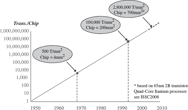
Figure 1.1 Moore's law (Moore 1965)
Like many other electronics industries, the creation and growth in the market has been driven by Moore's law (Moore 1965), represented pictorially in Figure 1.1. Moore's law shows that the number of transistors has been doubling every 18 months. The incredible growth has led to the creation of a number of markets and is the driving force between the markets of many electronics products such as mobile telephony, digital musical products, digital TV to name but a few. This is because not only have the number of transistors doubled at this rate, but the costs have not increased, thereby reducing the cost per transistor at every technology advance. This has meant that the FPGA market has grown from nothing in just over 20 years to being a key player in the IC industry with a market judged to be of the order of US $ 4.0 billion.
On many occasions, the growth indicated by Moore's law has led people to argue that transistors are essentially free and therefore can be exploited as in the case of programmable hardware, to provide additional flexibility. This could be backed up by the observation that the cost of a transistor has dropped from one-tenth of a cent in the 1980s to one-thousandth of a cent in the 2000s. This observation could be argued to have been validated by the introduction of hardware programmability into electronics in the form of FPGAs. In order to make a single transistor programmable in an SRAM technology, the programmability is controlled by storing a ‘1’ or a ‘0’ on the gate of the transistor, thereby making it conduct or not. This value is then stored in an SRAM cell which typically requires six transistors, involving a 600% increase for the introduction of programmability. The reality is that in an overall FPGA implementation, the penalty is nowhere as harsh as this, but it has to be taken into consideration in terms of ultimate system cost.
It is the ability to program the FPGA hardware after fabrication that is the main appeal of the technology as it provides a new level of reassurance in an increasingly competitive market where ‘right first time’ system construction is becoming more difficult to achieve. It would appear that assessment was vindicated as in the late 1990s and early 2000s, when there was a major market downturn, the FPGA market remained fairly constant when other microelectronic technologies were suffering. Of course, the importance of programmability has already been demonstrated by the microprocessor, but this represented a new change in how programmability was performed.
1.1.2 Programmability and DSP
The argument developed in the previous section presents a clear advantage of FPGA technology in terms of the use of its programmability to reduce the risk of incorrectly creating PCBs or evolving the manufactured product to later changes in standards. Whilst this might have been true in the early days of FPGA technology, evolution in silicon technology has moved the FPGA from being a programmable interconnection technology to making it into a system component. If the microprocessor or microcontroller was viewed as programmable system component, the current FPGA devices must also be viewed in this vein, giving us a different perspective on system programmability.
In electronic system design, the main attraction of microprocessors/microcontrollers is that it considerably lessens the risk of system development by reducing design complexity. As the hardware is fixed, all of the design effort can be concentrated on developing the code which will make the hardware work to the required system specification. This situation has been complemented by the development of efficient software compilers which have largely removed the need for designer to create assembly language; to some extent, this can absolve the designer from having a detailed knowledge of the microprocessor architecture (although many practitioners would argue that this is essential to produce good code). This concept has grown in popularity and embedded microprocessor courses are now essential parts of any electrical/electronic or computer engineering degree course.
A lot of this process has been down to the software developer's ability to exploit an underlying processor architecture, the Von Neumann architecture. However, this advantage has also been the limiting factor in its application to the topic of this text, namely digital signal processing (DSP). In the Von Neumann architecture, operations are processed sequentially, which allows relative straightforward interpretation of the hardware for programming purposes; however, this severely limits the performance in DSP applications which exhibit typically, high levels of parallelism and in which, the operations are highly data independent – allowing for optimisations to be applied. This cries out for parallel realization and whilst DSP microprocessors (here called DSPμs) go some way to addressing this situation by providing concurrency in the form of parallel hardware and software ‘pipelining’, there is still the concept of one architecture suiting all sizes of the DSP problem.
This limitation is overcome in FPGAs as they allow what can be considered to be a second level of programmability, namely programming of the underlying processor architecture. By creating an architecture that best meets the algorithmic requirements, high levels of performance in terms of area, speed and power can be achieved. This concept is not new as the idea of deriving a system architecture to suit algorithmic requirements has been the cornerstone of application-specific integrated circuit or ASIC implementations. In high volumes, ASIC implementations have resulted in the most cost effective, fastest and lowest energy solutions. However, increasing mask costs and impact of ‘right first time’ system realization have made the FPGA, a much more attractive alternative. In this sense, FPGAs capture the performance aspects offered by ASIC implementation, but with the advantage of programmability usually associated with programmable processors. Thus, FPGA solutions have emerged which currently offer several hundreds of gigaoperations per second (GOPS) on a single FPGA for some DSP applications which is at least an order of magnitude better performance than microprocessors.
Section 1.2 puts this evolution in perspective with the emergence of silicon technology by considering the history of the microchip. It highlights the key aspect of programmability which is discussed in more detail in Section 1.3 and leads into the challenges of exploiting the advantages offered by FPGA technology in Section 1.4.
1.2 A Short History of the Microchip
Many would argue that the industrial revolution in the late 1700s and early 1800s had a major social impact on how we lived and travelled. There is a strong argument to suggest that the emergence of the semiconductor market has had a similar if not more far-reaching impact on our lives. Semiconductor technology has impacted how we interact with the world and each other through technologies such as mobile telephony, e-mail, videoconferencing, are entertained via TV, radio, digital video, are educated through the existence of computer-based learning, electronic books; and also how we work with remote working now possible through wireless communications and computer technology.
This all started with the first transistor that was discovered by John Bardeen and Walter Brattain whilst working for William Shockley in Bell Laboratories. They were working with the semiconductor material silicon, to investigate its properties, when they observed that controlling the voltage on the ‘base’ connector, would control the flow of electrons between the emitter and collector. This had a considerable impact for electronics, allowing the more reliable transistor to replace the vacuum tube and leading to a number of ‘transistorized’ products.
Another major evolution occurred in the development of the first silicon chip, invented independently by Jack Kilby and Robert Noyce, which showed it was possible to integrate components on a single block of semiconductor material hence the name integrated circuit. In addition, Noyce's solution resolved some practical issues, allowing the IC to be more easily mass produced. There were many advantages to incorporating transistor and other components onto a single chip from a manufacturing and design point-of-view. For example, there was no more need for separate components with manually assembled wires to connect them. The circuits could be made smaller and the manufacturing process could be automated. The evolution of the chip led to the development of the standard TTL 7400 series components pioneered by Texas Instruments and the building components of many basic electronics kits. It was not known at the time, but these chips would become a standard in themselves.
Another key innovation was the development of the first microprocessor, the Intel 4004 by Bob Noyce and Gordon Moore in 1968. It had just over 2300 transistors in an area of only 12 mm2 which can be compared with today's 64-bit microprocessors which have 5.5 million transistors performing hundreds of millions of calculations each second. The key aspect was that by changing the programming code within the memory of the microprocessor, the function could be altered without the need to create a new hardware platform. This was fundamental to freeing engineers from the concept of building design by components which could not be easily changed to having a programmable platform where the functionality could be changed by altering the program code. It was later in 1965 in (Moore 1965) that Gordon Moore made the famous observation that has been coined as Moore's law. The original statement indicated that the complexity for minimum component costs has increased at a rate of roughly a factor of two per year, although this was later revised to every 18 months. This is representative of the evolution of silicon technology that allows us to use transistors, not only to provide functionality in processing data, but simply to create the overhead to allow us to provide programmability. Whilst this would suggest we could use transistors freely and that the microprocessor will dominate, the bottom line is that we are not using these transistors efficiently. There is an overall price to be paid for this in terms of the power consumed, thus affecting the overall performance of the system. In microprocessor systems, only a very small proportion of the transistors are performing useful work towards the computation.
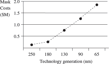
Figure 1.2 Mask cost versus technology generation (Zuchowski et al. 2002)
At this stage, a major shift in the design phase opened up the IC design process to a wide range of people, including university students (such as the main author at that time!). Mead and Conway (1979) produced a classic text which considerably simplified the IC design rules, allowing small chips to be implemented even without the need for design rule checking. By making some worst case assumptions, they were able to create a much smaller design rule set which could, given the size of the chips at that time, be performed manually. This lead to the ‘demystifying’ of the chip design process and with the development of software tools, companies were able to create ASICs for their own products. This along with the MOSIS program in the US (Pina 2001), provided a mechanism for IC design to be taught and experienced at undergraduate and postgraduate level in US universities. Later, the Eurochip program now known as Europractice (Europractice 2006) provided the same facility allowing a considerable number of chips to be fabricated and design throughout European universities. However, the ASIC concept was being strangled by increasing nonrecurrent engineering (NRE) costs which meant that there was an increased emphasis on ‘right first time’ design. These NRE costs were largely governed by the cost of generating masks for the fabrication process; these were increasing as it was becoming more expensive (and difficult) to generate the masks for finer geometries needed by shrinking silicon technology dimensions. This issue has become more pronounced as illustrated in the graph of Figure 1.2, first listed in Zuchowski et al. (2002) which gives the increasing cost (part of the NRE costs) needed to generate the masks for an ASIC.
The FPGA concept emerged in 1985 with the XC2064™ FPGA family from Xilinx. At the same time, a company called Altera were also developing a programmable device, later to become EP1200 device which was the first high-density programmable logic device (PLD). Altera's technology was device which was the first high-density programmable logic device (PLD). Altera's technology was manufactuured using 3-μm CMOS erasable programmable read-only-memory (EPROM) technology and required ultraviolet light to erase the programming whereas Xilinx's technology was based on conventional static RAM technology and required an EPROM to store the programming. The co-founder of Xilinx, Ross Freeman argued that with continuously improving silicon technology, transistors were going to increasingly get cheaper and could be used to offer programmability. This was the start of an FPGA market which was then populated by quite a number of vendors, including Xilinx, Altera, Actel, Lattice, Crosspoint, Algotronix, Prizm, Plessey, Toshiba, Motorola, and IBM. The market has now grown considerably and Gartner Dataquest indicated a market size growth to 4.5 billion in 2006, 5.2 billion in 2007 and 6.3 billion in 2008. There have been many changes in the market. This included a severe rationalization of technologies with many vendors such as Crosspoint, Algotronix, Prizm, Plessey, Toshiba, Motorola, and IBM disappearing from the market and a reduction in the number of FPGA families as well as the emergence of SRAM technology as the dominant technology largely due to cost. The market is now dominated by Xilinx and Altera and more importantly, the FPGA has grown from being a simple glue logic component to representing a complete System on Programmable Chip (SoPC) comprising on-board physical processors, soft processors, dedicated DSP hardware, memory and high-speed I/O.
In the 1990s, energy considerations became a key focus and whilst by this time, FPGAs had heralded the end of the gate array market, ASIC was still seen for the key mass market areas where really high performance and/or energy considerations were seen as key drivers such as mobile communications. Thus graphs comparing performance metrics for FPGA, ASIC and processor were generated and used by each vendor to indicate design choices. However, this is simplistic and a number of other technologies have emerged over the past decade and are described in Section 1.2.1.
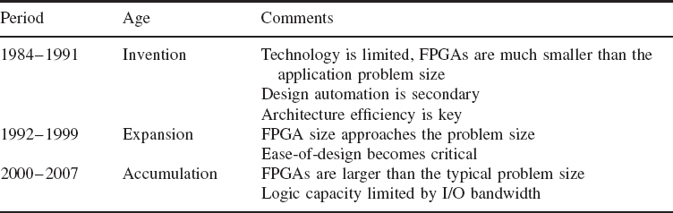
The FPGA evolution was neatly described by Steve Trimberger given in his plenary talk (Trimberger 2007) and summarized in Table 1.1. It indicates three different eras of evolution of the FPGA. The age of invention where FPGAs startedtoemerge and were beingusedas system components typically to provide programmable interconnect giving protection to design evolutions and variations as highlighted in Section 1.1. At this stage, design tools were primitive, but designers were quite happy to extract the best performance by dealing with LUTs or single transistors. In the early 1990s, there was a rationalization of the technologies described in the earlier paragraphs and referred to by Trimberger as the great architectural shakedown where the technology was rationalized. The age of expansion is where the FPGA started to approach the problem size and thus design complexity was key. This meant that it was no longer sufficient for FPGA vendors to just produce place and route tools and so it was critical that HDL-based flows were created. The final evolution period is described as the period of accumulation where FPGA started to incorporate processors and high-speed interconnection. This is described in detail in Chapter 5 where the recent FPGA offerings are reviewed.
1.2.1 Technology Offerings
In addition to FPGAs, ASICs and microprocessors, a number of other technologies emerged over the past decade which are worth consideration. These include:
Reconfigurable DSP processors. These types of processors allow some form of customization whilst providing a underlying fixed type of architecture that provides some level of functionality for the application required. Examples include the Xtensa processor family from Tensilica (Tensilica Inc. 2005) and D-Fabrix from Elixent (now Panasonic) which is a reconfigurable semiconductor intellectual property (IP) (Elixent 2005)
Structure ASIC implementation It could be argued that the concept of ‘gate array’ technology has risen again in the form of structured ASIC which is a predefined silicon framework where the user provides the interconnectivity in the form of reduced silicon fabrication. This option is also offered by Altera through their Hardcopy technology (Altera Corp. 2005), allowing users to migrate their FPGA design direct to ASIC.
The current situation is that quite a number of these technologies that now co-exist are targeted at different markets. This section has highlighted how improvements in silicon technologies have seen the development of new technologies which now form the electronic hardware for developing systems, in our case, DSP systems.
A more interesting viewpoint is to consider the availability of programmability in these technologies. The mask cost issue highlighted in Figure 1.2, along with the increasing cost of fabrication facilities, paints a depressing picture for developing application-specific solutions. This would tend to suggest that dedicated silicon solutions will be limited to mass market products and will only be able to exploited by big companies who can take the risk. Nanotechnology is purported to be a solution, but this will not be viable within the next decade in the authors' opinion. Structured ASIC could be viewed as a re-emergence of the gate array technology (at least in terms of the concept of constructing the technology) and will provide an interesting solution for low-power applications. However, the authors would argue that the availability of programmability will be central to next generation systems where time-to-market, production costs and pressures of right-first-time hardware are becoming so great that the concept of being able to program hardware will be vital. The next section attempts to compare technologies with respect to programmability.
1.3 Influence of Programmability
In many texts, Moore's law is used to highlight the evolution of silicon technology. Another interesting viewpoint particularly relevant for FPGA technology, is Makimoto's wave which was first published in the January 1991 edition of Electronics Weekly. It is based on an observation by Tsugio Makimoto who noted that technology has shifted between standardization and customization (see Figure 1.3). In the early 1960s, a number of standard components were developed, namely the Texas Instruments 7400 TTL series logic chips and used to create applications. In the early 1970s, the custom LSI era was developed where chips were created (or customized) for specific applications such as the calculator. The chips were now increasing in their levels of integration and so the term medium-scale integration (MSI) was born. The evolution of the microprocessor in the 1970s saw the swing back towards standardization where one ‘standard’ chip was used for a wide range of applications. The 1980s then saw the birth of ASICs where designers could overcome the limitations of the sequential microprocessor which posed severe limitations in DSP applications where higher levels of computations were needed. The DSP processor also emerged, such as the TMS32010, which differed from conventional processors as they were based on the Harvard architecture which had separate program and data memories and separate buses. Even with DSP processors, ASICs offered considerable potential in terms of processing power and more importantly, power consumption. The emergence of the FPGA from a ‘glue component’ that allows other components to be connected together to form a system to becoming a system component or even a system itself, led to increased popularity. The concept of coupling microprocessors with FPGAs in heterogeneous platforms was considerably attractive as this represented a completely programmable platform with microprocessors to implement the control-dominated aspects of DSP systems and FPGAs to implement the data-dominated aspects. This concept formed the basis of FPGA-based custom computing machines (FCCMs) which has led to the development of several conferences in the area and formed the basis for ‘configurable’ or reconfigurable computing (Villasenor and Mangione-Smith 1997). In these systems, users could not only implement computational complex algorithms in hardware, but use the programmability aspect of the hardware to change the system functionality allowing the concept of ‘virtual hardware’ where hardware could ‘virtually’ implement systems, an order of magnitude larger (Brebner 1997). The concept of reconfigurable systems is reviewed in Chapter 14.
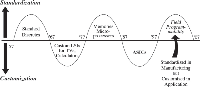
Figure 1.3 Makimoto's wave. Reproduced by permission of Reed Business Information
We would argue that there have been two programmability eras with the first era occurring with the emergence of the microprocessor in the 1970s, where engineers could now develop programmable solutions based on this fixed hardware. The major challenge at this time was the software environments; developers worked with assembly language and even when compilers and assemblers emerged for C, best performance was achieved by hand coding. Libraries started to appear which provided basic common I/O functions, thereby allowing designers to concentrate on the application. These functions are now readily available as core components in commercial compiler and assemblers. Increasing the need for high-level languages grew and now most programming is carried out in high-level programming languages such as C and Java with an increased use of even higher level environments such as UML.
The second era of programmability is offered by FPGAs. In the diagram, Makimoto indicates that the field programmability is standardized in manufacture and customized in application. This can be considered to have offered hardware programmability if you think in terms of the first wave as the programmability in the software domain where the hardware remains fixed. This is a key challenge as most of computer programming tools work on the principle of fixed hardware platform, allowing optimizations to be created as there is a clear direction on how to improve performance from an algorithmic representation. With FPGAs, the user is given full freedom to define the architecture which best suits the application. However, this presents a problem in that each solution must be handcrafted and every hardware designer knows the issues in designing and verifying hardware designs!
Some of the trends in the two eras have similarities. In the earlier days, schematic capture was used to design early circuits which was synonymous with assembly level programming. Hardware description languages such as VHDL and Verilog then started to emerge that could used to produce a higher level of abstraction with the current aim to have C-based tools such as SystemC and CatapultC from Mentor Graphics as a single software based programming environment. Initially as with software programming languages, there was a mistrust in the quality of the resulting code produced by these approaches. However with the establishment of improved cost-effective, synthesis tools which was equivalent to evolution of efficient software compilers for high-level programming languages, and also the evolution of library functions, a high degree of confidence was subsequently established and use of HDLs is now commonplace for FPGA implementation. Indeed, the emergence of IP cores mirrored the evolution of libraries such as I/O programming functions for software flows where common functions were reused as developers trusted the quality of the resulting implementation produced by such libraries, particularly as pressures to produce more code within the same time-span grew with evolving technology. The early IP cores emerged from basic function libraries into complex signal processing and communications functions such as those available from the FPGA vendors and various IP web-based repositories.
1.4 Challenges of FPGAs
In the early days, FPGAs were seen as glue logic chips used to plug components together to form complex systems. FPGAs then increasingly came to be seen as complete systems in themselves, as illustrated in Table 1.1. In addition to technology evolution, a number of other considerations accelerated this. For example, the emergence of the FPGA as a DSP platform was accelerated by the application of distributed arithmetic (DA) techniques (Goslin 1995, Meyer-Baese 2001). DA allowed efficient FPGA implementations to be realized using the LUT-based/adder constructs of FPGA blocks and allowed considerable performance gains to be gleaned for some DSP transforms such as fixed coefficient filtering and transform functions such as fast Fourier transform (FFT). Whilst these techniques demonstrated that FPGAs could produce highly effective solutions for DSP applications, the concept of squeezing the last aspect of performance out of the FPGA hardware and more importantly, spending several person months to create such innovative designs, was now becoming unacceptable. The increase in complexity due to technology evolution, meant that there was a growing gap in the scope offered by current FPGA technology and the designer's ability to develop solutions efficiently using currently available tools. This was similar to the ‘design productivity gap’ (IRTS 1999) identified in the ASIC industry where it was viewed that ASIC design capability was only growing at 25% whereas Moore's law growth was 60%. The problem is not as severe in FPGA implementation as the designer does not have to deal with sub-micrometre design issues. However, a number of key issues exist and include:
Understanding how to map DSP functionality into FPGA. Some of the aspects are relatively basic in this arena, such as multiplications, additions and delays being mapped onto on-board multipliers, adder and registers and RAM components respectively. However, the understanding of floatingpoint versus fixed-point, word length optimization, algorithmic transformation cost functions for FPGA and impact of routing delay are issues that must be considered at a system level and can be much harder to deal with at this level.
Design languages. Currently hardware description languages such as VHDL and Verilog and their respective synthesis flows are well established. However, users are now looking at FPGAs with the recent increase in complexity resulting in the integration of both fixed and programmable microprocessors cores as a complete system, and looking for design representations that more clearly represent system description. Hence there is an increased EDA focus on using C as a design language, but other representations also exist such as those methods based on models of computations (MoCs) such as synchronous dataflow.
Development and use of IP cores. With the absence of quick and reliable solutions to the design language and synthesis issues, the IP market in SoC implementation has emerged to fill the gap and allow rapid prototyping of hardware. Soft cores are particularly attractive as design functionality can be captured using HDLs and efficiently translated into the FPGA technology of choice in a highly efficient manner by conventional synthesis tools. In addition, processor cores have been developed which allow dedicated functionality to be added. The attraction of these approaches are that they allow application specific functionality to be quickly created as the platform is largely fixed.
Design flow. Most of the design flow capability is based around developing FPGA functionality from some form of higher-level description, mostly for complex functions. The reality now is that FPGA technology is evolving at such a rate that systems comprising FPGAs and processors are starting to emerge as a SoC platform or indeed, FPGAs as a single SoC platform as they have on-board hard and soft processors, high-speed communications and programmable resource, and this can be viewed as a complete system. Conventionally, software flows have been more advanced for processors and even multiple processors as the architecture is fixed. Whilst tools have developed for hardware platforms such as FPGAs, there is a definite need for software for flows for heterogeneous platforms, i.e. those that involve both processors and FPGAs.
These represent the challenges that this book aims to address and provide the main focus for the work that is presented.
References
Altera Corp. (2005) Hardcopy structured asics: Asic gain without the paint. Web publication downloadable from http://www.altera.com.
Brebner G (1997) The swappable logic unit. Proc. IEEE Symp. on FPGA-based Custom Computing Machines, Napa, USA, pp. 77–86.
Elixent (2005) Reconfigurable algorithm processing (rap) technology. Web publication downloadable from http://www.elixent.com/.
Europractice (2006) Europractice activity report. Web publication downloadable from http://europracticeic.com/documents_annual_reports.php.
Goslin G (1995) Using xilinx FPGAs to design custom digital signal processing devices. Proc. DSPX, pp. 565–604.
IRTS (1999) International Technology Roadmap for Semiconductors, 1999 edn. Semiconductor Industry Association. http://public.itrs.net
Maxfield C (2004) The Design Warrior's Guide to FPGAs. Newnes, Burlington.
Mead C and Conway L (1979) Introduction to VLSI Systems. Addison-Wesley Longman, Boston.
Meyer-Baese U (2001) Digital Signal Processing with Field Programmable Gate Arrays. Springer, Germany.
Moore GE (1965) Cramming more components onto integrated circuits. Electronics. Web publication downloadable from ftp://download.intel.com/research/silicon/moorespaper.pdf.
Pina CA (2001) Mosis: IC prototyping and low volume production service Proc. Int. Conf. on Microelectronic Systems Education, pp. 4–5.
Tensilica Inc. (2005) The Xtensa 6 processor for soc design. Web publication downloadable from http://www.tensilica.com/.
Trimberger S (2007) FPGA futures: Trends, challenges and roadmap IEEE Int. Conf. on Field Programmable Logic.
Villasenor J and Mangione-Smith WH (1997) Configurable computing. Scientific American, pp. 54–59.
Zuchowski P, Reynolds C, Grupp R, Davis S, Cremen B and Troxel B (2002) A hybrid ASIC and FPGA architecture. IEEE/ACM Int. Conf. on Computer Aided Design, pp. 187–194.