
One key to successful assembly language programming is knowing the environment you are programming for. The biggest part of that environment is the processor. Knowing the hardware platform your program will run on is crucial to being able to exploit both basic and advanced functions of the processor. Often, the whole point of using assembly language is to exploit low-level features of the processor within your application program. Knowing what elements can be used to assist your programs in gaining the most speed possible can mean the difference between a fast application and a slow application.
At the time of this writing, the most popular processor platform by far used in workstations and servers is the Intel Pentium family of processors. The hardware and instruction code set designed for the Pentium processors is commonly referred to as the IA-32 platform.
This chapter describes the hardware elements that make up the Intel IA-32 platform. The first part of the chapter describes the basic components found in the IA-32 processor platforms. Then the chapter describes the advanced features found in the newer Pentium 4 processor chips in the IA-32 family. Finally, the different processors that are contained within the IA-32 platform are discussed, showing what features to watch out for with the different types of processors, both from Intel and from other manufacturers.
While different processor families incorporate different instruction sets and capabilities, there is a core set of components that can be found on most processors. Most introductory computer science classes teach four basic components of a computer. Figure 2-1 shows a basic block diagram of these core components.
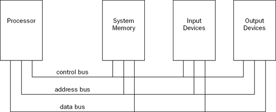
The processor contains the hardware and instruction codes that control the operation of the computer. It is connected to the other elements of the computer (the memory storage unit, input devices, and output devices) using three separate buses: a control bus, an address bus, and a data bus.
The control bus is used to synchronize the functions between the processor and the individual system elements. The data bus is used to move data between the processor and the external system elements. An example of this would be reading data from a memory location. The processor places the memory address to read on the address bus, and the memory storage unit responds by placing the value stored in that memory location on the data bus for the processor to access.
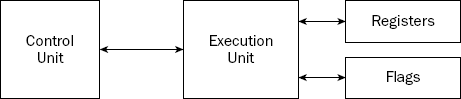
The processor itself consists of many components. Each component has a separate function in the processor's ability to process data. Assembly language programs have the ability to access and control each of these elements, so it is important to know what they are. The main components in the processor are as follows:
Control unit
Execution unit
Registers
Flags
Figure 2-2 shows these components and how they interact within the processor.
The following sections describe each of the core components, and how they are implemented in the IA-32 platform.
At the heart of the processor is the control unit. The main purpose of the control unit is to control what is happening at any time within the processor. While the processor is running, instructions must be retrieved from memory and loaded for the processor to handle. The job of the control unit is to perform four basic functions:
Retrieve instructions from memory.
Decode instructions for operation.
Retrieve data from memory as needed.
Store the results as necessary.
The instruction counter retrieves the next instruction code from memory and prepares it to be processed. The instruction decoder is used to decode the retrieved instruction code into a micro-operation. The micro-operation is the code that controls the specific signals within the processor chip to perform the function of the instruction code.
When the prepared micro-operation is ready, the control unit passes it along to the execution unit for processing, and retrieves any results to store in an appropriate location.
The control unit is the most hotly researched part of the processor. Many advances in microprocessor technology fall within the control unit section. Intel has made numerous advancements in speeding up the operations within the control unit. One of the most beneficial advancements is the manner in which instructions are retrieved and processed by the control unit.
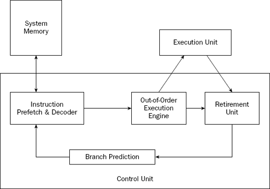
At the time of this writing, the latest Intel processor (the Pentium 4) uses a control unit technology called NetBurst. The NetBurst technology incorporates four separate techniques to help speed up processing in the control unit. Knowing how these techniques operate can help you optimize your assembly language programs. The NetBurst features are as follows:
Instruction prefetch and decoding
Branch prediction
Out-of-order execution
Retirement
These techniques work together to make the control unit of the Pentium 4 processor. Figure 2-3 shows how these elements interact.
The following sections describe each of these techniques as implemented in the Pentium 4 processor.
Older processors in the IA-32 family fetched instructions and data directly from system memory as they were needed by the execution unit. Because it takes considerably longer to retrieve data from memory than to process it, a backlog occurs, whereby the processor is continually waiting for instructions and data to be retrieved from memory. To solve this problem, the concept of prefetching was created.
Although the name sounds odd, prefetching involves attempting to retrieve (fetch) instructions and/or data before they are actually needed by the execution unit. To incorporate prefetching, a special storage area is needed on the processor chip itself—one that can be easily accessed by the processor, quicker than normal memory access. This was solved using pipelining.
Pipelining involves creating a memory cache on the processor chip from which both instructions and data elements can be retrieved and stored ahead of the time that they are required for processing. When the execution unit is ready for the next instruction, that instruction is already available in the cache and can be quickly processed. This is demonstrated in Figure 2-4.
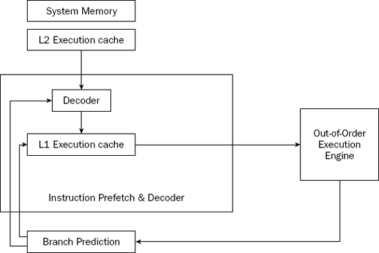
The IA-32 platform implements pipelining by utilizing two (or more) layers of cache. The first cache layer (called L1) attempts to prefetch both instruction code and data from memory as it thinks it will be needed by the processor. As the instruction pointer moves along in memory, the prefetch algorithm determines which instruction codes should be read and placed in the cache. In a similar manner, if data is being processed from memory, the prefetch algorithm attempts to determine what data elements may be accessed next and also reads them from memory and places them in cache.
Of course, one pitfall to caching instructions and data is that there is no guarantee that the program will execute instructions in a sequential order. If the program takes a logic branch that moves the instruction pointer to a completely different location in memory, the entire cache is useless and must be cleared and repopulated with instructions from the new location.
To help alleviate this problem, a second cache layer was created. The second cache layer (called L2) can also hold instruction code and data elements, separate from the first cache layer. When the program logic jumps to a completely different area in memory to execute instructions, the second layer cache can still hold instructions from the previous instruction location. If the program logic jumps back to the area, those instructions are still being cached and can be processed almost as quickly as instructions stored in the first layer cache.
While assembly language programs cannot access the instruction and data caches, it is good to know how these elements work. By minimizing branches in programs, you can help speed up the execution of the instruction codes in your program.
While implementing multiple layers of cache is one way to help speed up processing of program logic, it still does not solve the problem of "jumpy" programs. If a program takes many different logic branches, it may well be impossible for the different layers of cache to keep up, resulting in more last-minute memory access for both instruction code and data elements.
To help solve this problem, the IA-32 platform processors also incorporate branch prediction. Branch prediction uses specialized algorithms to attempt to predict which instruction codes will be needed next within a program branch.
Special statistical algorithms and analysis are incorporated to determine the most likely path traveled through the instruction code. Instruction codes along that path are prefetched and loaded into the cache layers.
The Pentium 4 processor utilizes three techniques to implement branch prediction:
Deep branch prediction enables the processor to attempt to decode instructions beyond multiple branches in the program. Again, statistical algorithms are implemented to predict the most likely path the program will take throughout the branches. While this technique is helpful, it is not totally foolproof.
Dynamic data flow analysis performs statistical real-time analysis of the data flow throughout the processor. Instructions that are predicted to be necessary for the flow of the program but not reached yet by the instruction pointer are passed to the out-of-order execution core (described next). In addition, any instructions that can be executed while the processor is waiting for data related to another instruction are processed.
Speculative execution enables the processor to determine what distant instruction codes not immediately in the instruction code branch are likely to be required, and attempt to process those instructions, again using the out-of-order execution engine.
The out-of-order execution engine is one of the greatest improvements to the Pentium 4 processor in terms of speed. This is where instructions are prepared for processing by the execution unit. It contains several buffers to change the order of instructions within the pipeline to increase the performance of the control unit. This is demonstrated in Figure 2-5.
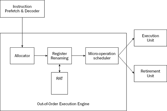
Instructions retrieved from the prefetch and decoding pipeline are analyzed and reordered, enabling them to be executed as quickly as possible. By analyzing a large number of instructions, the out-of-order execution engine can find independent instructions that can be executed (and their results saved) until required by the rest of the program. The Pentium 4 processor can have up to 126 instructions in the out-of-order execution engine at any one time.
There are three sections within the out-of-order execution engine:
The allocator
Register renaming
The micro-operation scheduler
The allocator is the traffic cop for the out-of-order execution engine. Its job is to ensure that buffer space is allocated properly for each instruction that the out-of-order execution engine is processing. If a needed resource is not available, the allocator will stall the processing of the instruction and allocate resources for another instruction that can complete its processing.
The register renaming section allocates logical registers to process instructions that require register access. Instead of the eight general-purpose registers available on the IA-32 processor (described later in the "Registers" section), the register renaming section contains 128 logical registers. It maps register requests made by instructions into one of the logical registers, to allow simultaneous access to the same register by multiple instructions. The register mapping is done using the register allocation table (RAT). This helps speed up processing instructions that require access to the same register sets.
The micro-operation scheduler determines when a micro-operation is ready for processing by examining the input elements that it requires. Its job is to send micro-operations that are ready to be processed to the retirement unit, while still maintaining program dependencies. The micro-operation scheduler uses two queues to place micro-operations in—one for micro-operations that require memory access and one for micro-operations that do not. The queues are tied to dispatch ports. Different types of Pentium processors may contain a different number of dispatch ports. The dispatch ports send the micro-operations to the retirement unit.
The retirement unit receives all of the micro-operations from the pipeline decoders and the out-of-order execution engine and attempts to reassemble the micro-operations into the proper order for the program to properly execute.
The retirement unit passes micro-operations to the execution unit for processing in the order that the out-of-order execution engine sends them, but then monitors the results, reassembling the results into the proper order for the program to execute.
This is accomplished using a large buffer area to hold micro-operation results and place them in the proper order as they are required.
When a micro-operation is completed and the results placed in the proper order, the micro-operation is considered retired and is removed from the retirement unit. The retirement unit also updates information in the branch prediction unit to ensure that it knows which branches have been taken, and which instruction codes have been processed.
The main function of the processor is to execute instructions. This function is performed in the execution unit. A single processor can actually contain multiple execution units, capable of processing multiple instruction codes simultaneously.
The execution unit consists of one or more Arithmetic Logic Units (ALUs) The ALUs are specifically designed to handle mathematical operations on different types of data. The Pentium 4 execution unit includes separate ALUs for the following functions:
The low-latency integer execution unit is designed to quickly perform simple integer mathematical operations, such as additions, subtractions, and Boolean operations. Pentium 4 processors are capable of performing two low-latency integer operations per clock cycle, effectively doubling the processing speed.
The complex-integer execution unit handles more involved integer mathematical operations. The complex-integer execution unit handles most shift and rotate instructions in four clock cycles. Multiplication and division operations involve long calculation times, and often take 14 to 60 clock cycles.
The floating-point execution unit differs between the different processors in the IA-32 family. All Pentium processors can process floating-point mathematical operations using the standard floating-point execution unit. Pentium processors that contain MMX and SSE support also perform these calculations in the floating-point execution unit.
The floating-point execution unit contains registers to handle data elements that contain 64-bit to 128-bit lengths. This enables larger floating-point values to be used in calculations, which can speed up complex floating-point calculations, such as digital signal processing and video compression.
Most of the operations of the processor require processing data. Unfortunately, the slowest operations a processor can undertake are trying to read or store data in memory. As shown in Figure 2-1, when the processor accesses a data element, the request must travel outside of the processor, across the control bus, and into the memory storage unit. This process is not only complicated, but also forces the processor to wait while the memory access is being performed. This downtime could be spent processing other instructions.
To help solve this problem, the processor includes internal memory locations, called registers. The registers are capable of storing data elements for processing without having to access the memory storage unit. The downside to registers is that a limited number of them are built into the processor chip.
The IA-32 platform processors have multiple groups of registers of different sizes. Different processors within the IA-32 platform include specialized registers. The core groups of registers available to all processors in the IA-32 family are shown in the following table.
Register | Description |
|---|---|
General purpose | Eight 32-bit registers used for storing working data |
Segment | Six 16-bit registers used for handling memory access |
Instruction pointer | A single 32-bit register pointing to the next instruction code to execute |
Eight 80-bit registers used for floating-point arithmetic data | |
Control | Five 32-bit registers used to determine the operating mode of the processor |
Debug | Eight 32-bit registers used to contain information when debugging the processor |
The following sections describe the more common registers in greater detail.
The general-purpose registers are used to temporarily store data as it is processed on the processor. The general-purpose registers have evolved from the old 8-bit 8080 processor days to 32-bit registers available in the Pentium processors. Each new version of general-purpose registers is created to be completely backwardly compatible with previous processors. Thus, code that uses 8-bit registers on the 8080 chips is still valid on 32-bit Pentium chips.
While most general-purpose registers can be used for holding any type of data, some have acquired special uses, which are consistently used in assembly language programs. The following table shows the general-purpose registers available on the Pentium platform, and what they are most often used for.
Register | Description |
|---|---|
EAX | Accumulator for operands and results data |
EBX | Pointer to data in the data memory segment |
ECX | Counter for string and loop operations |
EDX | I/O pointer |
EDI | Data pointer for destination of string operations |
ESI | Data pointer for source of string operations |
ESP | Stack pointer |
EBP | Stack data pointer |
The 32-bit EAX, EBX, ECX, and EDX registers can also be referenced by 16-bit and 8-bit names to represent the older versions of the registers. Figure 2-6 shows how the registers can be referenced.
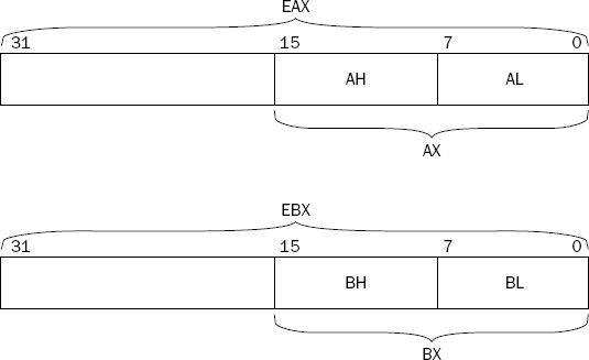
By using the reference AX, the lower 16 bits of the EAX register are used. By using the reference AL, the lower 8 bits of the EAX register are used. AH references the next 8 higher bits after AL.
The segment registers are used specifically for referencing memory locations. The IA-32 processor platform allows three different methods of accessing system memory:
Flat memory model
Segmented memory model
Real-address mode
The flat memory model presents all system memory as a contiguous address space. All instructions, data, and the stack are contained in the same address space. Each memory location is accessed by a specific address, called a linear address.
The segmented memory model divides the system memory into groups of independent segments, referenced by pointers located in the segment registers. Each segment is used to contain a specific type of data. One segment is used to contain instruction codes, another data elements, and a third the program stack.
Memory locations in segments are defined by logical addresses. A logical address consists of a segment address and an offset address. The processor translates a logical address to a corresponding linear address location to access the byte of memory.
The segment registers are used to contain the segment address for specific data access. The following table describes the available segment addresses.
Segment Register | Description |
|---|---|
CS | Code segment |
DS | Data segment |
SS | Stack segment |
ES | Extra segment pointer |
FS | Extra segment pointer |
GS | Extra segment pointer |
Each segment register is 16 bits and contains the pointer to the start of the memory-specific segment. The CS register contains the pointer to the code segment in memory. The code segment is where the instruction codes are stored in memory. The processor retrieves instruction codes from memory based on the CS register value, and an offset value contained in the EIP instruction pointer register. A program cannot explicitly load or change the CS register. The processor assigns its value as the program is assigned a memory space.
The DS, ES, FS, and GS segment registers are all used to point to data segments. By having four separate data segments, the program can help separate data elements, ensuring that they do not overlap. The program must load the data segment registers with the appropriate pointer value for the segments, and reference individual memory locations using an offset value.
The SS segment register is used to point to the stack segment. The stack contains data values passed to functions and procedures within the program.
If a program is using the real address mode, all of the segment registers point to the zero linear address, and are not changed by the program. All instruction codes, data elements, and stack elements are accessed directly by their linear address.
The instruction pointer register (or EIP register), sometimes called the program counter, keeps track of the next instruction code to execute. While this sounds like a simple process, with the implementation of the instruction prefetch cache it is not. The instruction pointer points to the next instruction to execute.
An application program cannot directly modify the instruction pointer per se. You cannot specify a memory address and place it in the EIP register. Instead, you must use normal program control instructions, such as jumps, to alter the next instruction to be read into the prefetch cache.
In a flat memory model, the instruction pointer contains the linear address of the memory location for the next instruction code. If the application is using a segmented memory model, the instruction pointer points to a logical memory address, referenced by the contents of the CS register.
The five control registers are used to determine the operating mode of the processor, and the characteristics of the currently executing task. The individual control registers are described in the following table.
Control Register | |
|---|---|
CR0 | System flags that control the operating mode and states of the processor |
CR1 | Not currently used |
CR2 | Memory page fault information |
CR3 | Memory page directory information |
CR4 | Flags that enable processor features and indicate feature capabilities of the processor |
The values in the control registers cannot be directly accessed, but the data contained in the control register can be moved to a general-purpose register. Once the data is in a general-purpose register, an application program can examine the bit flags in the register to determine the operating status of the processor and/or currently running task.
If a change is required to a control register flag value, the change can be made to the data in the general-purpose register, and the register moved to the control register. Systems programmers usually modify the values in the control registers. Normal user application programs do not usually modify control registers entries, although they might query flag values to determine the capabilities of the host processor chip on which the application is running.
For each operation that is performed in the processor, there must be a mechanism to determine whether the operation was successful or not. The processor flags are used to perform this function.
Flags are important to assembly language programs, as they are the only means available to determine whether a program's function succeeded or not. For example, if an application performed a subtraction operation that resulted in a negative value, a special flag within the processor would be set. Without checking the flag, the assembly language program would not have any way to know that something went wrong.
The IA-32 platform uses a single 32-bit register to contain a group of status, control, and system flags. The EFLAGS register contains 32 bits of information that are mapped to represent specific flags of information. Some bits are reserved for future use, to allow additional flags to be defined in future processors. At the time of this writing, 17 bits are used for flags.
The flags are divided into three groups based on function:
The following sections describe the flags found in each group.
The status flags are used to indicate the results of a mathematical operation by the processor. The current status flags are shown in the following table.
Flag | Bit | Name |
|---|---|---|
CF | 0 | Carry flag |
PF | 2 | Parity flag |
AF | 4 | Adjust flag |
ZF | 6 | Zero flag |
SF | 7 | Sign flag |
OF | 11 | Overflow flag |
The carry flag is set if a mathematical operation on an unsigned integer value generates a carry or a borrow for the most significant bit. This represents an overflow condition for the register involved in the mathematical operation. When an overflow occurs, the data remaining in the register is not the correct answer to the mathematical operation.
The parity flag is used to indicate whether the result register in a mathematical operation contains corrupt data. As a simple check for validity, the parity flag is set if the total number of 1 bits in the result is even, and is cleared if the total number of 1 bits in the result is odd. By checking the parity flag, an application can determine whether the register has been corrupted since the operation.
The adjust flag is used in Binary Coded Decimal (BCD) mathematical operations (see Chapter 7, "Using Numbers"). The adjust flag is set if a carry or borrow operation occurs from bit 3 of the register used for the calculation.
The zero flag is set if the result of an operation is zero. This is most often used as an easy way to determine whether a mathematical operation results in a zero value.
The sign flag is set to the most significant bit of the result, which is the sign bit. This indicates whether the result is positive or negative.
The overflow flag is used in signed integer arithmetic when a positive value is too large, or a negative value is too small, to be properly represented in the register.
Control flags are used to control specific behavior in the processor. Currently, only one control flag is defined, the DF flag, or direction flag. It is used to control the way strings are handled by the processor.
When the DF flag is set (set to one), string instructions automatically decrement memory addresses to get the next byte in the string. When the DF flag is cleared (set to zero), string instructions automatically increment memory addresses to get the next byte in the string.
The system flags are used to control operating system–level operations. Application programs should never attempt to modify the system flags. The system flags are listed in the following table.
Flag | Bit | Name |
|---|---|---|
TF | 8 | Trap flag |
IF | 9 | Interrupt enable flag |
IOPL | 12 and 13 | I/O privilege level flag |
NT | 14 | Nested task flag |
RF | 16 | Resume flag |
VM | 17 | Virtual-8086 mode flag |
AC | 18 | Alignment check flag |
VIF | 19 | Virtual interrupt flag |
VIP | 20 | Virtual interrupt pending flag |
ID | 21 | Identification flag |
The trap flag is set to enable single-step mode. In single-step mode, the processor performs only one instruction code at a time, waiting for a signal to perform the next instruction. This feature is extremely useful when debugging assembly language applications.
The interrupt enable flag controls how the processor responds to signals received from external sources.
The I/O privilege field indicates the I/O privilege level of the currently running task. This defines access levels for the I/O address space. The privilege field value must be less than or equal to the access level required to access the I/O address space; otherwise, any request to access the address space will be denied.
The nested task flag controls whether the currently running task is linked to the previously executed task. This is used for chaining interrupted and called tasks.
The resume flag controls how the processor responds to exceptions when in debugging mode.
The virtual-8086 flag indicates that the processor is operating in virtual-8086 mode instead of protected or real mode.
The alignment check flag is used (along with the AM bit in the CR0 control register) to enable alignment checking of memory references.
The virtual interrupt flag replicates the IF flag when the processor is operating in virtual mode.
The virtual interrupt pending flag is used when the processor is operating in virtual mode to indicate that an interrupt is pending.
The ID flag is interesting in that it indicates whether the processor supports the CPUID instruction. If the processor is able to set or clear this flag, it supports the CPUID instruction. If not, then the CPUID instruction is not available.
The core features of the IA-32 platform mentioned so far are available on all of the processors in the family, starting with the 80386 processor. This section describes some advanced features that the assembly language programmer can utilize when creating programs specifically designed for the Pentium processors.
Early processors in the IA-32 family required a separate processor chip to perform floating-point mathematical operations. The 80287 and 80387 processors specialized in providing floating-point arithmetic operations for the computer chips. Programmers who needed fast processing of floating-point operations were forced to turn to additional hardware to support their needs.
Starting with the 80486 processor, the advanced arithmetic functions found in the 80287 and 80387 chips were incorporated into the main processor. To support these functions, additional instruction codes as well as additional registers and execution units were required. Together these elements are referred to as the x87 floating-point unit (FPU).
The x87 FPU incorporates the following additional registers:
FPU Register | |
|---|---|
Eight 80-bit registers for floating-point data | |
16-bit register to report the status of the FPU | |
Control register | 16-bit register to control the precision of the FPU |
16-bit register to describe the contents of the eight data registers | |
48-bit FPU instruction pointer (FIP) points to the next FPU instruction | |
48-bit FPU data pointer (FDP) points to the data in memory | |
11-bit register to hold the last instruction processed by the FPU |
The FPU registers and instruction codes enable assembly language programs to quickly process complex floating-point mathematical functions, such as those required for graphics processing, digital signal processing, and complex business applications. The FPU can process floating-point arithmetic considerably faster than the software simulation used in the standard processor without the FPU. Whenever possible, the assembly language programmer should utilize the FPU for floating-point arithmetic.
The Pentium II processor introduced another method for programmers to perform complex integer arithmetic operations. MMX was the first technology to support the Intel Single Instruction, Multiple Data (SIMD) execution model.
The SIMD model was developed to process larger numbers, commonly found in multimedia applications. The SIMD model uses expanded register sizes and new number formats to speed up the complex number crunching required for real-time multimedia presentations.
The MMX environment includes three new floating-point data types that can be handled by the processor:
64-bit packed byte integers
64-bit packed word integers
64-bit packed doubleword integers
These data types are described in detail in Chapter 7, "Using Numbers." To handle the new data formats, MMX technology incorporates the eight FPU registers as special-purpose registers. The MMX registers are named MM0 through MM7, and are used to perform integer arithmetic on the 64-bit packed integers.
While the MMX technology improved processing speeds for complex integer arithmetic, it did nothing for programs that require complex floating-point arithmetic. That problem was solved with the SSE environment.
The next generation of SIMD technology was implemented starting with the Pentium III processor. SSE enhances performance for complex floating-point arithmetic, often used in 3-D graphics, motion video, and video conferencing.
The first implementation of SSE in the Pentium III processor incorporated eight new 128-bit registers (called XMM0 through XMM7) and a new data type—a 128-bit packed single-precision floating point. The SSE technology also incorporated additional new instruction codes for processing up to four 128-bit packed single-precision floating-point numbers in a single instruction.
The second implementation of SSE (SSE2) in the Pentium 4 processors incorporates the same XMM registers that SSE uses, and also introduces five new data types:
128-bit packed double-precision floating point
128-bit packed byte integers
128-bit packed word integers
128-bit packed doubleword integers
128-bit packed quadword integers
These data types are also described in detail in Chapter 7. The new data types and the corresponding instruction codes enable programmers to utilize even more complex mathematical operations within their programs. The 128-bit double-precision floating-point data types allow for advanced 3-D geometry techniques, such as ray tracing, to be performed with minimal processor time.
A third implementation of SSE (SSE3) does not create any new data types, but provides several new instructions for processing both integer and floating-point values in the XMM registers.
One of the most exciting features added to the Pentium 4 processor line is hyperthreading. Hyperthreading enables a single IA-32 processor to handle multiple program execution threads simultaneously.
The hyperthreading technology consists of two or more logical processors located on a single physical processor. Each logical processor contains a complete set of general-purpose, segment, control, and debug registers. All of the logical processors share the same execution unit. The out-of-order execution core is responsible for handling the separate threads of instruction codes provided by the different logical processors.
Most of the advantages of hyperthreading appear at the operating system level. Multitasking operating systems, such as Microsoft Windows and the various UNIX implementations, can assign application threads to the individual logical processors. To the application programmer, hyperthreading may not appear to be that much of a benefit.
At the time of this writing, the IA-32 family of processors is the most popular computing platform used in desktop workstations and many server environments. The most popular operating system that utilizes the IA-32 platform is Microsoft Windows, although other popular operating systems run on the IA-32 platform, such as Novell file servers, and UNIX-based OSs such as Linux and the BSD derivatives.
While many advances in the IA-32 processor platform have been made throughout the years, many features are common to all IA-32 processors. The features mentioned in this chapter form the core of all assembly language programs written for the IA-32 platform. However, knowing the special features available on a particular processor can help speed your assembly language program along very nicely. This section describes the different processors available in the IA-32 family, and how their features must be taken into consideration when programming for the platform.
Of course, Intel is the main supplier of processors in the IA-32 platform. In today's computing environment, the most commonly used processor platform is the Pentium processor. It is extremely unusual to encounter hardware from the earlier IA-32 processors, such as the 80486 processor.
Unfortunately, several different types of Pentium processors are still active in businesses, schools, and homes. Creating assembly language programs that utilize advanced IA-32 features found only on the latest processors may limit your application's marketability. Conversely, if you know that your programming environment consists of a specific type of processor, utilizing available features may help give your application the performance boost needed to smoke the competition.
This section describes the different types of Pentium processors commonly available in workstations and servers, highlighting the features that are available with each processor.
The core of the Pentium processor line is, of course, the base Pentium processor. The Pentium processor was introduced in 1993 as a replacement for the 80486 processor. The Pentium processor was the first processor to incorporate the dual execution pipeline, and was the first processor to use a full 32-bit address bus and 64-bit internal data path.
While the performance benefits of the Pentium processor were obvious, from a programming point of view, the Pentium processor did not provide any new features beyond the 80486 architecture. All of the core registers and instruction codes from the 80486 processor were supported, including the internal FPU support.
The P6 processor family was introduced in 1995 with the Pentium Pro processor. The Pentium Pro processor incorporated a completely new architecture from the original Pentium processor. The P6 family of processors were the first to utilize a superscalar microarchitecture, which greatly increased performance by enabling multiple execution units and instruction prefetch pipelines.
The Pentium MMX and Pentium II processors, part of the P6 family, were the first processors to incorporate MMX technology, and also introduced new low-power states that enabled the processor to be put in sleep mode when idling. This feature helped conserve power, and became the ideal platform for laptop computing devices.
The Pentium III processor was the first processor to incorporate SSE technology, enabling programmers to perform complex floating-point arithmetic operations both quickly and easily.
The Pentium 4 processor was introduced in 2000, and again started a new trend in microprocessor design. The Pentium 4 utilizes the Intel NetBurst architecture, which provides extremely fast processing speeds by incorporating the instruction pipelines, the out-of-order execution core, and execution units.
The Pentium 4 processor supports SSE3, a more advanced SSE technology that implements additional floating-point operations to support high-speed multimedia computations.
While the IA-32 platform is often considered to be an Intel thing, there are many other non-Intel processors available on the market that also implement the IA-32 features. It is possible that your assembly language application may be run on a non-Intel platform, so it is important that you understand some differences between the platforms.
Today, Intel's biggest competitor is AMD. AMD has released a competing processor chip for every release of Intel's Pentium processor. It is not uncommon to run across Microsoft Windows workstations using AMD processors. The following table shows the AMD processor's history.
AMD Processor | Equivalent to | Notes |
|---|---|---|
K5 | Pentium | 100% software compatible |
K6 | Pentium MMX | Pentium with full MMX support |
K6-2 | Pentium II | Uses 3D Now technology |
K6-III | Pentium III | |
Athlon | Pentium 4 | |
Athlon XP | Pentium 4 w/SSE |
For the assembly language programmer, the most important difference between AMD and Intel processors is apparent when using SIMD technology. While AMD has duplicated the MMX technology, it has not fully duplicated the newer SSE technology. When Intel introduced SSE in the Pentium II processor, AMD took a different route. The AMD K6-2 processor uses a different SIMD technology called 3D Now. The 3D Now technology uses similar registers and data types as SSE, but it is not software compatible. This has caused high-speed programmers considerable difficulty when programming for SSE functions.
With the release of the Athlon XP processor in 2001, AMD supported SSE integer arithmetic. At the time of this writing, the newest AMD processor chips now fully support SSE technology.
While the Cyrix corporation has not been in business for a few years, their IA-32 platform processors still live on in many workstations and low-end servers. It is still possible to run across a Cyrix processor in various environments.
The evolution of the Cyrix processor family mirrored the Intel processors for many versions. The first Pentium-grade processor produced by Cyrix was originally called the 6x86 processor. It is 100 percent software compatible with the Pentium processor. When Intel introduced MMX technology, Cyrix produced the 6x86MX processor (they didn't have a license to call it MMX, but MX was close enough).
When Cyrix was sold to the VIA chipset company, the original Cyrix processor line was renamed. The 6x86 processor was called the M1, and the 6x86MX processor was called M2. Again, these processors retained their compatibility with their Pentium counterparts.
Before the demise of the Cyrix processor, one final version made it to market. Dubbed the Cyrix III, it was also compatible with the Pentium III processor. Unfortunately, similar to AMD, it too had to support SSE using the 3D Now technology, which made it incompatible with assembly language programs written for SSE.
Before writing an assembly language program, you must know the target processor used when the program is executed. The most popular processor platform in use today is the Intel IA-32 platform. This platform includes the Pentium family of processors from Intel, as well as the Athlon processors from AMD.
The flagship of the IA-32 platform is the Intel Pentium 4 processor. It incorporates the NetBurst architecture to quickly and easily process instructions and data. The core of the NetBurst architecture includes a control unit, an execution unit, registers, and flags.
The control unit controls how the execution unit processes instructions and data. Speed is accomplished by prefetching and decoding instructions from memory long before the execution unit processes them. Instructions can also be processed out of order and the results stored until they are needed in the application.
The execution unit in a Pentium 4 processor has the capability of processing multiple instructions concurrently. Simple integer processes are performed quickly and stored in the out-of-order area in the control unit until needed. Complex integer and floating-point processes are also streamlined to increase performance.
Registers are used as local data storage within the processor to prevent costly memory access for data. The IA-32 platform processors provide several general-purpose registers for holding data and pointers as the program is executed. Instructions are retrieved from memory based on the value of the instruction pointer register. The control register controls the processor's behavior.
A special register containing several flags determines the status and operation of the processor. Each flag represents a different operation within the processor. Status flags indicate the result of operations performed by the processor. Control flags control how the processor behaves for specific operations. System flags determine operating system behavior, and should not be touched by application programmers.
Innovation in the IA-32 platform is alive and well. Many new features have been introduced in recent processor releases. The floating-point unit (FPU) has been incorporated into Pentium processors to assist in floating-point mathematical operations.
To further support complex mathematical processing, the Single Instruction, Multiple Data (SIMD) technology enables the processing of large numerical values in both integer and floating-point form. The Multimedia Extensions (MMX) enable programmers to use 64-bit integers in high-precision integer calculations. Following that, the Streaming SIMD Extensions (SSE) technology enables programmers to use 128-bit single-precision floating-point values, and subsequently, the SSE2 technology enables the use of 128-bit double-precision floating-point data values. These new data types greatly speed up the processing of mathematically intensive programs, such as those used for multimedia processing and digital signal processing.
When programming for the IA-32 platform, you should be aware of the different processors available, and know what functions each processor type supports. The core of the IA-32 platform is the original Pentium processor. It supports the core IA-32 registers and instruction sets, along with simple built-in FPU support. Similar to the Pentium processor, AMD produced the K5 processor, and Cyrix produced the 6x86 processor. Each of these processors is 100 percent software compatible with the IA-32 instruction code set.
Intel introduced MMX functionality in the Pentium II processor line. Following suit, AMD incorporated MMX features in the K6 processor, and Cyrix with the 6x86MX processor. All of these processors include the MMX registers, and the additional MMX instruction codes.
The SSE technology is where things get complicated in the IA-32 world. The Pentium II processor introduced SSE registers and instruction sets, but unfortunately, other processor manufacturers were not able to directly incorporate these features. Instead, AMD and Cyrix implemented the 3D Now technology in their K6-2 (AMD) and Cyrix III (Cyrix) processors. The 3D Now technology provided the same 64-bit integer data types as SSE, but the instruction codes were different.
At the time of this writing, the Pentium 4 processor is the flagship processor for Intel. It supports SSE3 technology, as well as the NetBurst architecture. The AMD rival is the Athlon XP, which now incorporates SSE registers and instruction sets, making it software compatible with the Pentium 4 processor.
Now that you have an understanding of the hardware platform used in this book, it's time to examine the software development environment. The next chapter discusses the assembly language tools that are available in the Linux operating system environment. By using Linux, you can leverage the GNU development tools to create a professional software development environment with minimal cost.