
12
Wireless Communications Systems Design and Considerations
A wireless communication system designer requires a wide range of requirements and conditions. One decision in one design step is closely related to another decision in the next design step. Thus, it is very difficult to optimize many metrics such as complexity (or area in a chip), throughput, latency, power consumption, and flexibility because many of them are trade-off relationship. A wireless communication system designer often makes a decision subjectively and empirically. In this chapter, we take a look at considerations when designing wireless communications systems. We mainly deal with wireless communication system design flows and considerations, a high level view of wireless communication systems, several implementation techniques, and hardware/software codesign.
12.1 Wireless Communications Systems Design Flow
A brief design flow of wireless communications systems is as follows: Firstly, the international regulator such as the International Telecommunication Union (ITU) defines the spectrum allocation for different services such as satellite services, land mobile services, and radar services. The regional regulatory bodies such as European Conference of Postal and Telecommunications Administrations (CEPT) in Europe and Federal Communications Commission (FCC) in the United States play quite important role in the decision making process in the ITU. They build a regional consensus even if there are national representatives in ITU meetings. After spectrum allocation for a certain service, the ITU may label certain allocations for a certain technology and determine the requirements for the technology. For the requirements, some standardization bodies such as the 3rd Generation Partnership Project (3GPP) and the Institute of Electrical and Electronics Engineers (IEEE) make their contributions to the ITU, where they guarantee that their technology will meet the requirements. The actual technology is specified in the internal standardization such as 3GPP and IEEE. Some standards are established at the regional level. The regulators are responsible for spectrum licensing and protection. Secondly, a wireless channel is defined. Its mathematical model is developed and the test scenario is planned for the evaluation of the proposed technical solutions or algorithms. For example, short-range wireless channel models are different from cellular channel models. In cellular systems, we basically use empirical channel models such as ITU channel models. Their test scenarios are different as well. Thirdly, each block of wireless communication systems is selected to satisfy the requirements of wireless communication systems. This step is discussed and defined in wireless communication standards such as 3GPP and IEEE. The next steps are wireless communication system implementation. They are carried out by enterprises. Fourthly, receiver algorithms under the given standard are developed (or selected) and their performances are confirmed by a floating point design. Basically, standard bodies define interfaces, signaling protocols, and data structures. They give us the requirements of the transmitter and receiver. In addition, we can roughly obtain key algorithms of the transmitter and receiver from the given standard. However, many freedoms for actual design and implementation are left. Fifthly, a fixed point design is performed. In this step, the wireless communication system architecture is defined. The performance (complexity, latency, etc.) of the wireless communication system can be roughly calculated. Lastly, conventional chip design processes as the remaining steps (RTL design and back-end design) are performed.
We dealt with key wireless communications algorithms in Part II and each algorithm can be implemented in widely different ways. We have many options to assemble these algorithms in various architectures from a general purpose microprocessor to a full-custom chip. Depending on system requirements such as latency, power consumption, and cost, we decide the wireless communication system structure including flexibility, parallelism, pipelining, and time sharing and choose the system parameters including supply voltage, clock rate, and word lengths. The comprehensive design requires a wide range of data and one decision in one design step is closely related to another decision in the next design step. We need to optimize many metrics such as complexity (or area in a chip), throughput, latency, power consumption, and flexibility. Many of them are trade-off relationship. It is very complex and difficult to find an optimal solution. Thus, mobile phone vendors or network equipment vendors optimize their products based on their own design know-how.
The hardware system design can be classified into front-end design and back-end design. The front-end design deals with all logical design and verification. Each algorithm is verified by a floating point simulation. In this step, the full-chain wireless communication system models (including error correction coding, modulation, FFT/IFFT, etc.) provide us with their system performances such as BER or capacity. As the next step, a fixed-point simulation is carried out in consideration of a bit level. We can obtain a further refined result of their system performances. These simulations are developed by software tools such as Matlab or C++. Sometime System-C or System Verilog can be used for a cycle-accurate model. After verifying system performances, a Register-Transfer Level (RTL) design is performed using hardware description languages such as Verilog or VHSIC Hardware Description Language (VHDL). In this step, we implement each algorithm as hardware registers and logic operations and then integrate all blocks. If the function and logic works correctly, we move to the back-end design which deals with system development and fabrication. An RTL from the front-end design is converted to a gate level by synthesis tools such as Cadence, Synopsys, and Mentor Graphics. A netlist as a result of synthesis contains the used cells and area and their interconnections. It is used to create a physical layout by placement and routing tools. The back-end design process is too costly and time consuming. Many important parts of the back-end design are automated. Thus, the front-end design is getting more important in the modern hardware design. Figure 12.1 illustrates a typical front-end design flow.

Figure 12.1 Typical front-end design flow
In floating point simulation, a module-based approach is used. The module means any arithmetic operation, memory, interconnection, or each algorithm block. It provides us with accurate estimation of hardware complexity and cost. In addition, it is very helpful for optimization of the complex wireless communication system. Each wireless communication block is designed and pairwise verified at the transmitter and the receiver. If each block works correctly, we integrate and evaluate system performances. In fixed-point simulation, we start from bit level (or bit resolution/input bit quantization) decision of Analogue-to-Digital Converter (ADC) and Digital-to-Analogue Converter (DAC). The bit level decision affects the next blocks. The ADC/DAC is the first block of a whole baseband receiver/transmitter chain. Thus, the ADC bit level becomes a basis of all bit levels for each block. As the results of fixed-point simulation, the input/output bit level of each block and rough architecture become important information at the RTL design. The RTL design including the datapath flow and the control flow follows four steps. The first step is to capture behavior using a high-level state machine. The second step is to construct a data path with parameterized modules on the high-level state machine. The third step is to connect the data path to the controller. The last step is to convert the high-level state machine to the finite state machine. In the RTL design, we can find the critical path to meet system requirements and predict latency, complexity, power consumption, etc. The critical path enables us to identify system bottlenecks and share resources to improve system performances. In addition, a hardware designer decides the system architecture including parallelism, pipelining, and time sharing. In each step of the front-end design, it is very important to provide a hardware designer with a feedback. Thus, the architecture and parameter should be iteratively improved to meet the system requirements. If we obtain a netlist as the result of the RTL design, we can proceed to the back-end design step. Figure 12.2 illustrates a typical back-end design flow. The detailed back-end design flow depends on software tool, methodology, and the technology libraries by a fabrication house. Basically, the design period at a floating point simulation step is much shorter than at a lower level design step. We make further efforts on this step and analyze high-level decisions. If we consider a rapid prototyping, the optimization as well as the system design is carried out in this step. In this step, it is difficult to estimate accurate complexity and power consumption. There are many constraints to optimize performance, complexity, latency, power consumption, etc. Thus, the trade-off of high-level decision is inevitable. For example, the trade-off between flexibility and efficiency is one important decision point. A general purpose device such as a Central Processing Unit (CPU) is flexible but not efficient. On the other hand, a dedicated device such as a baseband chipset is efficient but not flexible. The general purpose device is useful when we need to compute a general task. However, the baseband chipset has an inherent property of the wireless communication system and does not need the full flexibility. Most of wireless communication algorithms are datapath intensive design block. Thus, we exploit many signal processing optimization techniques such as parallel processing, pipelining, and windowing.

Figure 12.2 Typical back-end design flow
If a target application is decided, a high level-design starts from algorithm choice, architecture selection, and implementation parameter decision. For example, when designing the turbo decoder with a low complexity and latency, we may choose Max-log MAP decoders or soft output Viterbi decoders as a component decoder instead of log MAP decoders, select a sliding window decoder architecture, and adopt the 3bits soft input/output. As we discussed in Chapter 6, there is a trade-off between complexity and performance. In terms of BER performance, the log MAP algorithm and 4bits soft input/output would be a better choice. Basically, there are many algorithm blocks and a designer should make a decision in consideration of system requirements and performance. Thus, a design methodology for high-level design is needed. There are some design guidelines and methodologies in public but many chip vendors have their own design guidelines based on their know-how.
12.2 Wireless Communications Systems Design Considerations
Now, we take a look into wireless communications system design considerations and several implementation techniques. The first design consideration is bit-level (bit resolution or word length) decision. The bit-level directly affects to system complexity and performance. For example, if we increase one bit from 3 bits soft input/output to 4 bits soft input/output in the turbo decoder, the memory size and each sub-block complexity such as branch metric calculation and path metric calculation must be increased. In addition, the bit-level is highly related to vulnerability and sensitivity regarding noise and nonlinearity. Thus, it results in performance degradation. The floating point representation uses an integer but the fixed point representation supports a fixed range. When dealing with the fixed point representation, we should manage a finite precision error caused by truncation and overflow. We start making the bit-level decision from ADC/DAC to the next blocks sequentially. The suitable decision of the bit-level is based on a trade-off between performance and complexity. The final decision should be made through a full-chain simulation and feedback from other design steps.
The second design consideration is the number of computation. It is tightly coupled with power consumption and latency as well as complexity. This is the basic step to estimate the number of operations such as multiplication, addition, shift register, and memory. Based on this estimation, we can have the initial approximation about system complexity. In addition, the initial power consumption and latency can be estimated if we have a basic architecture and component. The architecture and component choice is highly related to the system complexity and performance. For example, when we need a memory for a baseband chip, a register is fast but expensive. On the other hands, Static Random Access Memory (SRAM) is less fast and cheaper than a register. Figure 12.3 illustrates simple comparison of memory types.

Figure 12.3 Memory comparisons
The third design consideration is algorithm type and property. There are many algorithm types such as recursive algorithms, backtracking algorithms, greedy algorithms, divide and conquer algorithms, dynamic programming algorithms, and brute force algorithms. Depending on algorithm types, we use different resources and it affects the process of building the corresponding architecture. For example, a recursive algorithm requires simple computation and high interconnection power. Thus, we focus on global interconnection, connectivity ratio, and memory management rather than computational logic. In Ref. [1], property metrics are investigated and classified as follows: size, topology, timing, concurrency, uniformity, temporal locality, spatial locality, and regularity.
- Size is the amount of computation and includes the number of data transfers, operations, and variables.
- Topology is the relative arrangement of operations.
- Timing includes latency, critical path delay, and scheduling.
- Concurrency is the ability of parallel processing.
- Uniformity is how evenly resource accesses are distributed.
- Temporal locality is the persistence of computation’s variables.
- Spatial locality is the communication pattern among blocks and how well the computation is partitionable into clusters of operations with interconnections.
- Regularity is how often common patterns appear.
Those metrics are highly related to system performance and help us to optimize system design. Among them, the concurrency is very important and measures how many operations can be simultaneously executed. Depending on the level of parallelism, the effective sampling rate is decided. For example, we consider a discrete time Finite Impulse Response (FIR) filter as follows:
where y[n] and x[n] are the output signal and the input signal, respectively. The coefficients a, b, and c are the values of the impulse response. We can convert the sequential FIR filter into the three parallel FIR filter as follows:

The parallel systems receive three inputs (x [3k], x[3k+1], and x[3k+2]) at the kth clock cycle and produces three outputs (y[3k], y[3k+1], and y[3k+2]) as shown in Figure 12.4.
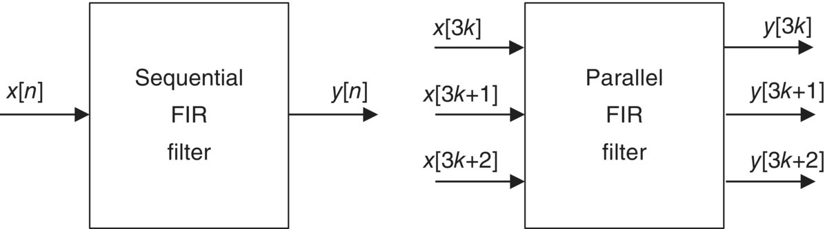
Figure 12.4 Sequential system and parallel system
In the parallel system, the same operation is duplicated in order to achieve faster processing. Thus, we should increase the area (or complexity). Another important property metric is the timing metrics. Especially, this is critical metric when we develop a high-speed baseband chipset. There are many metrics about timing. The most important metric is the critical path which creates the longest delay. The critical path can be found in linear time with a modified shortest path algorithm [2]. For example, Figure 12.5 illustrates one example of data flow graph. In this figure, the critical path is six clock cycles. The inverse of the critical path is tightly coupled with the maximum throughput of the system.

Figure 12.5 Example of critical path in data flow graph
Another important metric is the latency. The definition of the latency in Very-Large-Scale Integration (VLSI) design is a little bit different from its wireless communication systems. In wireless communication systems, latency is defined as the time a signal takes to travel between a transmitter and a receiver. On the other hand, the latency in VLSI design means the time between input data and processed output data. It is often used to mean waiting time that increases actual response time beyond desired response time. The iteration of the system is key metric as well. It provides us with estimation of potential throughput improvement by pipelining and parallel processing. In Ref. [1], the iteration bound is defined as the maximum ratio (over all feedback cycles) of the total execution time, T(c), divided by the number of sample delays in the cycle, D(c), as follows:

If the system is non-recursive, the iteration bound is zero. The other metrics about timing are the longest path, maximum operator delay, and slacks for each operator type. The regularity is helpful for designing a structure. It is widely investigated in Refs[3–5]. Especially, the structured design is highly desirable when developing in a modular concept. In order to quantify the regularity, the percentage operation coverage by common patterns is defined in Ref. [1]. For example, it can be a set of patterns containing all chained pairs of associative operators. Figure 12.6 illustrates one example of FIR filter to quantify the regularity. In this figure, there are 10 operators (3 flip-flops, 4 multipliers, and 3 adders). We can observe 4 multiplication–addition patterns and they cover 7 out of 10 operations. Thus, the coverage of the multiplication–addition patterns is 70%.

Figure 12.6 Example of regularity metric

Figure 12.7 FIR filter
The fourth design consideration is architecture selection. There are many types of design architectures such as Digital Signal Processor (DSP), full-custom hardware, Application-Specific Integrated Circuit (ASIC), and Field Programmable Gate Arrays (FPGA). The DSP can be simply defined as a specialized microprocessor for signal processing applications. When comparing a DSP with a general purpose microprocessor, the DSP supports specialized instructions and multiple operations per instruction. Thus, it is more suitable for signal processing which requires high memory bandwidth, high energy efficiency, and math centric complex computation. In addition, the DSP is flexible because it is software that is programmed to perform a task. On the other hand, a full-custom chip is not a programmable hardware but a dedicated hardware. It supports a high degree of optimization in both area and performance. However, it is too much time-consuming due to manual layout design. Thus, it is almost extinct in the modern hardware design. The ASIC is a customized chip to perform a particular operation. It is suitable for communication or multimedia applications. There are mainly two types of ASICs: standard cell-based ASICs and gate-array based ASICs. The standard cell-based ASICs are also called cell-based IC (CBIC) or semi-custom where standard cell means a predesigned logic cell such as flip-flop, multiplexer, AND gate, and XOR gate. The standard cells are usually synthesized from an RTL description and inserted into a chip vendor own library. An ASIC designer uses the standard cells in a schematic and they are placed and routed by backend tools. Some standard cells such as memory and datapath are tiled to create macrocells. In addition, an ASIC vendor provides electrical characteristics such as propagation delay and capacitance to an ASIC designer. The ASIC is the most popular design architecture because it has much quicker design time than the full custom hardware design. However, one disadvantage is that the mask cost is increasingly expensive. The gate-array-based ASICs enable us to cut mask costs because the transistor level masks are fully defined and an ASIC designer can customize the metal connection for each design. Thus, it has a short fabrication time and low production cost. However, their disadvantages are (i) inefficient memory usage and (ii) slow and big logics due to fixed transistors and limited wiring space. The FPGAs can be classified into one of ASIC types. It is cheaper solution for small volumes. A FPGA designer programmes the basic logic cells and the interconnection to implement combinational logics and sequential logics. It contains the programmable logic cells and surrounds them by the programmable interconnection. The FPGA has two important advantages: flexibility and short design process. The flexibility allows us to reconfigure our design. We do not need layouts or masks. Thus, it provides us with simple design cycles and faster time to market. Most importantly, the development cost is low. On the other hand, the efficiency is low. Namely, unused logic cells and interconnections can exist. In addition, an internal memory is limited, power consumption is higher than the ASIC, analogue interface is challenging, and optimization is difficult. Thus, the FPGA is used as the prototype of the design before the ASIC implementation. Table 12.1 summarizes comparison of the design architectures.
Table 12.1 Comparison of design architectures
| Full-custom | Standard cell ASIC | FPGA | |
| Area | Compact | Compact to moderate | Large |
| Performance | High | High to moderate | Low |
| Cell size | Variable | Variable/fixed | Fixed |
| Interconnection | Variable | Variable | Programmable |
| Time to market | Long | Middle | Short |
| Development cost | High | Moderate | Low |
Once a wireless communication system design works satisfactorily, it can be implemented on one of the above architectures. When we select one of the above architectures, the flexibility and efficiency is the key criterion. Basically, the flexibility and efficiency is trade-off relationship. Figure 12.8 represents their relationship in terms of the flexibility and efficiency.

Figure 12.8 Flexibility vs. efficiency
The full-custom chip is implemented as the dedicated hardware. The efficiency of the full-custom chip design is high. The full-custom chip design can be significantly optimized. However, its flexibility is poor. On the other hand, a software design provides us with high flexibility but low efficiency. Hardware and software partition is very important matter in the wireless communication system design. Hardware and software codesign settles down in common design methodology. We will discuss this topic in the next section. When implementing wireless communication systems, a flexible architecture is one of the key issues because many wireless communication systems support multiple modes and variable parameters. For example, LTE downlink physical layer supports the multiple channel bandwidths (1.25, 2.5, 5, 10, 15, and 20 MHz) and the corresponding multiple FFT sizes (128, 256, 512, 1024, 1536, and 2048). Adaptive modulation coding is one essential technique of modern wireless broadband communications. Thus, the flexibility of the architecture is very important consideration and the receiver should be flexible enough to accommodate various transmission modes. Naturally, it is essential to implement efficiently. The area (or complexity) efficiency is directly related to cost. The energy efficiency is one key parameter to mobile devices. In terms of both flexibility and efficiency, the ASIC is good choice and widely used for the wireless communication system design. Basically, multiple functional blocks of a wireless communication system should be developed using an ASIC library. Several different teams are involved in each block design and they individually develop it using implementation techniques such as pipelining and parallel processing. In order to integrate each block, a top level system designer should figure out all inputs/outputs, timing, power consumption, and requirements of each block.
The fifth design consideration is implementation-type selection. The implementation type is selected according to the target application. If we develop a mobile device, we should focus on a low-power implementation in order to support a long battery life. If we consider a broadband communication system, we have to implement using a high-speed technique. If we develop Software Defined Radio (SDR), the flexibility is the most important design consideration. In this section, we investigate a low-power implementation and its techniques. A low-power implementation requires a holistic approach including collaboration with architecture level design, algorithm level design, physical design, power verification, and so on. First of all, we investigate the physical or circuit level design. In digital Complementary Metal Oxide Semiconductor (CMOS) design, the power consumption can be represented as follows:
In (12.5) and (12.6), the first term is the switching power consumption, where α is the activity factor (which means the probability a transition occurs) and f is the system clock frequency. If the signal rises and falls every cycle, ![]() . If it switches once per cycle,
. If it switches once per cycle, ![]() . In static gates, the activity factor typically is 0.1 [6]. C is the capacitive load. V is the voltage swing which is typically same as supply voltage. The second term is the internal power consumption. I
scc is the short circuit current. When transistors switch, the short circuit current arises. The third term is the leakage power consumption. I
leakage is the leakage current. It arises from subthreshold and gate. The typical value of the subthreshold leakage is 20 nA/µm for low V and 0.02 nA/µm for high V [6]. The typical value of the gate leakage is 3 nA/µm for thin oxide and 0.002 nA/µm for thick oxide[6]. In (12.6), the switching part represents the dynamic dissipation associated with charging and discharging of load capacitances. This is the dominant term of the power dissipation. Thus, the low-power implementation in circuit level is based on minimizing the capacitive load C and the voltage swing (supply voltage) V. In order to minimize them, we can use small transistors and short wires and adopt the lowest supply voltage. In addition, we can reduce the dynamic power using the lowest clock frequency. However, the lowest frequency increases a delay so that it is not suitable way to meet a high speed processing. Another approach is to reduce the static power by minimizing the leakage in a fabrication stage. The leakage power consumption is getting more dominant term of the total power dissipation. The power gating technique[7] is used to reduce the leakage power by shutting off the current to blocks which are not in use. The key design goal of this technique is to switch between a low power mode and an active mode at the appropriate time and in the appropriate way while minimizing the performance degradation. It is widely used in many mobile devices. Another important low-power technique is clock gating [7]. It is extensively used to reduce the dynamic power dissipation by reducing unnecessary clock activities. In synchronous digital circuits, the clock takes significant part (up to 40%) of power dissipation[8]. The supply voltage can be reduced by Adaptive Voltage Scaling (AVS) technique. The multiple critical paths are implemented on hardware (integrated circuit). We compare the delay on these critical paths with the required delay. If one delay is smaller than the required delay, the AVS reduces the supply voltage gradually with a given step until the value between the required delay and the delay of the critical path is in the AVS error margin. We can adjust both the clock frequency and the supply voltage by Dynamic Voltage and Frequency Scaling (DVFS) technique. In the first term of (12.6), the required supply voltage is determined by the frequency at which the circuit is clocked. Thus, a look-up table about the relationship between the supply voltage and the frequency is created by silicon measurement. We can define suitable pairs of the frequency and the supply voltage. A large number of voltage levels are dynamically switched according to the workloads. This technique is also commonly used to reduce power dissipation on a wide range of mobile devices.
. In static gates, the activity factor typically is 0.1 [6]. C is the capacitive load. V is the voltage swing which is typically same as supply voltage. The second term is the internal power consumption. I
scc is the short circuit current. When transistors switch, the short circuit current arises. The third term is the leakage power consumption. I
leakage is the leakage current. It arises from subthreshold and gate. The typical value of the subthreshold leakage is 20 nA/µm for low V and 0.02 nA/µm for high V [6]. The typical value of the gate leakage is 3 nA/µm for thin oxide and 0.002 nA/µm for thick oxide[6]. In (12.6), the switching part represents the dynamic dissipation associated with charging and discharging of load capacitances. This is the dominant term of the power dissipation. Thus, the low-power implementation in circuit level is based on minimizing the capacitive load C and the voltage swing (supply voltage) V. In order to minimize them, we can use small transistors and short wires and adopt the lowest supply voltage. In addition, we can reduce the dynamic power using the lowest clock frequency. However, the lowest frequency increases a delay so that it is not suitable way to meet a high speed processing. Another approach is to reduce the static power by minimizing the leakage in a fabrication stage. The leakage power consumption is getting more dominant term of the total power dissipation. The power gating technique[7] is used to reduce the leakage power by shutting off the current to blocks which are not in use. The key design goal of this technique is to switch between a low power mode and an active mode at the appropriate time and in the appropriate way while minimizing the performance degradation. It is widely used in many mobile devices. Another important low-power technique is clock gating [7]. It is extensively used to reduce the dynamic power dissipation by reducing unnecessary clock activities. In synchronous digital circuits, the clock takes significant part (up to 40%) of power dissipation[8]. The supply voltage can be reduced by Adaptive Voltage Scaling (AVS) technique. The multiple critical paths are implemented on hardware (integrated circuit). We compare the delay on these critical paths with the required delay. If one delay is smaller than the required delay, the AVS reduces the supply voltage gradually with a given step until the value between the required delay and the delay of the critical path is in the AVS error margin. We can adjust both the clock frequency and the supply voltage by Dynamic Voltage and Frequency Scaling (DVFS) technique. In the first term of (12.6), the required supply voltage is determined by the frequency at which the circuit is clocked. Thus, a look-up table about the relationship between the supply voltage and the frequency is created by silicon measurement. We can define suitable pairs of the frequency and the supply voltage. A large number of voltage levels are dynamically switched according to the workloads. This technique is also commonly used to reduce power dissipation on a wide range of mobile devices.
Secondly, we take a look at a low-power approach in terms of algorithm design. There are several ways to reduce the power consumption at the algorithm development stage: algorithm modifications, structure transformations of an algorithm, and appropriate arithmetic operation selection. In Part II, we discussed algorithm modifications. For example, the log-MAP algorithm is very complex so that it is very difficult to implement. Especially, the log term and the exponential term are very difficult to compute. Thus, we changed the log-MAP algorithm to the max-log-MAP algorithm. The simplified max-log-MAP algorithm has only compare operation even if slight performance degradation occurs. The structure transformations do not change the functional behavior of algorithm blocks and optimize computational modules/operations and their interconnection. In Ref.[9], several transformation techniques are introduced to reduce power consumption. They basically pay attention to the first term (switching part) of(12.6). They approach to reduce the power consumption for a fixed throughput by reducing the supply voltage through speed-up transformation and by minimizing the effective capacitance being switched through several transformations. The speed-up transformations reduce the required control steps so that it increases the degree of concurrency. It includes retiming, pipelining, unfolding, and algebraic transformation. The transformation to minimize the effective capacitance reduces the total required operations by optimizing resource usages. For example, when one feedback loop is the bottleneck of the system, we can use the retiming technique so that the feedback loop shortens the critical path and increases the degree of concurrency. This transformation results in the reduced voltage through pipelining. In Ref. [10], algorithm transformation techniques for a low-power wireless communication system design are described. We take a look at retiming, pipelining, folding, and so on. In order to apply the transformation techniques, we need to employ Data Flow Graph (DFG) representation. It is a directed graph to show the data dependencies between functions. The DFG is defined as follows:
where V is the set of graph nodes representing computation (function or subtask), E is the set of directed edges (or arcs) representing data path (connection between nodes), q is the set of node delays representing execution time of each node, and d is the set of edge weights representing associated delay. Figure 12.9 illustrates an example of one block diagram and corresponding DFG representation of FIR filter.

Figure 12.9 Block diagram (a) and DFG representation (b) of FIR filter
In Figure 12.9b, the node A and B represent multiplication and addition, respectively. Each set and element is defined as follows:
The node delay represents the required time to produce one sample output of the block. Now, we define several properties of the DFG as follows:
- The iteration represents an execution of each DFG node.
- Iteration period is the required time to perform the iteration. Intra-iteration and inter-iteration represent a direct edge without any delay and a direct edge with at least one delay, respectively. Figure 12.10 illustrates the iteration period.
- The critical path of the DFG is the path with the longest computation time among all paths containing no delay.
- The loop (cycle) means the directed path that begins and ends at the same node.
- The loop bound means the minimum time to execute one loop in the DFG and it is defined as follows:
where q(v) and d(e) represent the loop computation time and the number of delays in the loop, respectively.
- The critical loop represents the loop in which has the maximum loop bound.
- The iteration period bound
 is defined as follows:

where L is a loop in the DFG. It is not possible to achieve an iteration period less than the iteration period bound even if we have infinite hardware resource.

Figure 12.10 Iteration period

Figure 12.11 DFG of Example 12.2

Figure 12.12 Loops of DFG example
The retiming technique is a transformation technique moving delay from one edge to another edge in a DFG. It is used to reduce the total number of registers and improve scheduling of the DFG. Thus, we can reduce the power consumption and the critical path delay of the system. Figure 12.13 illustrates an example of retiming.

Figure 12.13 Before retiming (a) and after retiming (b)
In Figure 12.13b, one delay from the output of the node B is transferred to its inputs. In Figure 12.13a, the iteration period is 30 time units (=T m + T a) when the multiplication computation (T m) and the addition computation (T a) are 20 time units and 10 time units, respectively. After retiming as in Figure 12.13b, the iteration period is 20 time units (=max(T m,T a)).
The pipelining technique, as the name suggests, comes from the idea that a pipe can send water without waiting. It allows us to process new data before a prior data processing finishes. It reduces the critical path and increases sample speed by adding delays and retiming. Basically, parallel processing duplicates the same operation to achieve faster processing. However, the pipelining technique inserts latches or registers along the data path so that it can shorten the critical path. Figure 12.14 illustrates comparison of one logic system and its pipelined version. The pipelined system inserts one delay in the system and can achieve a higher throughput by reducing the critical path. However, the system has a longer latency due to the additional delay.

Figure 12.14 Combinational logic (a) and pipelined system (b)
Consider simple 2 adders with and without one delay as shown in Figure 12.15. Figure 12.15a does not show any delay (pipeline depth is 0) and the latency is zero. On the other hand, Figure 12.15b has one pipeline delay (pipeline depth is 1) and the latency is one. Their timing diagrams are shown in Figure 12.16.

Figure 12.15 Simple 2 adders system without one delay (a) and with one delay (b)

Figure 12.16 Timing diagram of 2 adders system with/without one delay
If the pipeline depth increases, the system throughput increases and the clock period decreases. Now, we need to consider where to put the delay. Basically, we place the pipeline delay across feed-forward cutsets. Cutset is a set of edges in the DFG such that if the edges are removed from the original DFG, the remaining DFG becomes two disjoint graphs. The feed-forward is the cutset when the data move in the forward direction on all the edge of the cutset. Figure 12.17 illustrates three feed-forward cutsets and delay placements in the feed-forward cutsets. In Figure 12.17a, the dash lines represent feed-forward cutsets but the dash-dot line is not feed forward cutset. When comparing the original FIR filter (Figure 12.17a) and the pipelined FIR filter (Figure 12.17b), the critical path has been changed from 40 time units (=T m + 2T a) to 30 time units (=T m + T a).

Figure 12.17 Feed-forward cutsets (a) and delay placements (b, c, and d)
The pipelining technique is very useful in a low power design. From(12.6), the switching (dynamic) power dissipation of a serial architecture is defined as follows:
where C tot is the total capacitance of the serial architecture. The propagation delayT pd is defined as follows:

where C c is a capacitance to be charged and discharged in the critical path, k is a transistor constant, and V t is a threshold voltage. When we consider an M pipeline depth, the pipelining technique reduces the critical path to 1/M. Thus, the capacitance C c is reduced to C c/M which means only C c/M is now charged and discharged. If the frequency f is maintained, the supply voltage can be reduced to βV where 0 < β < 1. The power dissipation of the pipelined system is
where β is determined by the propagation delay. The propagation delay of the pipelined system is

The same clock speed is maintained for both serial architecture and pipelined architecture. Thus, we can find β using the following equation:
From(12.16), we can observe that the power dissipation of the pipelined system is lower than the corresponding serial system.
The folding technique is very useful technique to improve area efficiency by time-multiplexing many operations to single functional units. The unfolding technique is the reverse of the folding technique. The folding technique inserts delays (registers) and reuse logics so that it saves areas. Figure 12.18 illustrates an example of two folding transformation. As we can see in the figure, we can reduce the number of operation.

Figure 12.18 Simple two adders system (a) and two folding transformation (b)
When we have N same patterns in the system, we can apply the folding transformation and reduce the hardware complexity by a factor of N. Instead, the computation time is increased by a factor of N.
In addition, algebraic transformations such distributivity, associativity, and commutativity are very useful for improving the efficiency. For example, one computation (X 1 × X 2) + (X 1 × X 3) can be reorganized as X 1 × (X 2 + X 3) using distributivity. We can reduce from two multipliers and one adder to one multiplier and one adder. Figure 12.19 illustrates algebraic transformations.

Figure 12.19 Algebraic transformations: distributivity (a), associativity (b), and commutativity (c)
12.3 Hardware and Software Codesign
We mainly dealt with a hardware design in Sections 12.1 and 12.2. However, the role of software is getting more important in the modern wireless communication system. Before 1990s, hardware and software (HW/SW) are developed independently and then integrated. The role of software in wireless communication devices was not significant and the interaction between hardware and software was very limited. However, as the performance of DSPs and microprocessors is improved, many tasks are implemented in software. HW/SW codesign emerged as a new system design discipline. The HW/SW codesign is the most efficient implementation. It improves an overall system performance and provides us with lower costs and smaller development cycle. Figure 12.20 illustrates classical system design flow and timeline. After receiving system specifications, we decide a HW architecture and partition HW tasks and SW tasks. Namely, we develop hardware first and then design software after fixing the hardware architecture. When both HW and SW are developed, we integrate them and verify the whole system.

Figure 12.20 Classical system design flow and timeline
This design flow is inefficient and requires a long design period. Basically, the development time depends on a target application, resource, and fabrication. However, the architecture definition and HW/SW partition typically requires 6–12 months. The HW design, SW design, and system integration typically require 24–48 months. The field test typically requires 6–12 months. One important reason why it takes so long is that the SW design begins when the HW architecture is fixed. Recently, the time-to-market is very important because mobile devices are outmoded very quickly. In addition, the classical system design flow does not provide enough interaction between HW and SW so that the system optimization is limited. On the other hand, the HW/SW codesign allows us to develop HW and SW concurrently and save the development time. In addition, the HW/SW codesign is based on iterative process. Thus, we can optimize a system more efficiently. Figure 12.21 illustrates HW/SW codesign flow and timeline.

Figure 12.21 HW/SW codesign flow and timeline
The main advantages of SW design are (i) short time-to-market and (ii) small design and verification costs. The main advantages of HW design are (i) good performance and (ii) high energy efficiency. The HW/SW codesign provides us with good balance between HW design and SW design and allows us to have their advantages.
As we can see in Figure 12.21, the first step of the HW/SW codesign is system specification and architecture definition. The specification is to define the functions of a system and clearly describe the behavior including concurrency, hierarchy, state transition, timing, etc. The architecture definition includes system modeling to refine the specification and produce a HW and SW model. In this step, it is important to have a unified HW/SW representation. The unified representation describes tasks of the system which can be implemented in HW or SW. It helps a HW designer and a SW designer to communicate with each other. In addition, it defines an architectural model as shown in Figure 12.22.

Figure 12.22 HW/SW codesign architecture
Many unified models have been developed and used to represent heterogeneous systems in the literatures [11–13]. Thus, the system can be modeled as data flow graphs, communicating processes, finite state machines, discrete event system, and Petri Nets. As we discussed in Section 12.2, the data flow graphs are very popular in modeling data driven systems because it easily models data and control flow and concurrent operations. The nodes of the data flow graphs correspond to operations in HW or SW. In Ref. [14], a system is described as a set of interactive processes executing each other. The process corresponds to either HW computations or SW computations in the system. This modeling method is well matched with high level simulation and synthesis. The Finite State Machine (FSM) is one of the most well-known models to describe control flow. We define a set of states, inputs, outputs, and functions in the model. It changes from one state to another state when a transition happens. Although the FSM provides us with good mathematical foundation, it is not suitable for a complex system because the system complexity increases exponentially as the number of states increases. In addition, it is difficult to represent concurrency of states. Thus, the FSM is not appropriate to model modern communication systems. A discrete event system can be defined as a discrete-state event-driven system. Its state evolution entirely depends on the occurrence of asynchronous discrete events over time [15]. An event occurs instantaneously and causes a transition from one state to another state. The state transitions in the time driven systems are synchronized by the clock. However, the state transition in the discrete event system happens as a result of asynchronous and concurrent event process. Thus, the events are labeled as a time and analyzed in chronological order. The discrete event system is useful for the unified HW/SW representation. However, the computational complexity is so high because it requires global time sorting for all events. A Petri net is a directed bipartite graph consisting of places, tokens, transitions, and arcs. The place describes conditions and holds tokens. The token represents data flow in the system. The transition represents an event and a transition firing indicates that an event has occurred. The arc moves between a place and a transition.
The second step is HW/SW partition. It is the key part of HW/SW codesign process because the partition affects the overall system performance, development time, and cost. The main purpose of HW/SW partition is to design a system to meet the required performance under the given constraints (cost, power, complexity, etc.). In this step, we have to consider many design parameters. Basically, we want to automate HW/SW partition but it is still difficult to have optimal HW/SW partition. Thus, we approach either software-oriented partition or hardware-oriented partition. The software-oriented partition is to assign all functions in software and then move time-critical parts into hardware. Thus, we can develop a flexible system at low cost. On the other hand, the hardware-oriented partition is to assign all functions in hardware and then move sequential, not-time-critical and flexible parts into software. Thus, we can build a high performance and high speed system. Both approaches are based on functional partitioning. It defines all functions of the system and then implements the system. Thus, it provides us with a better trade-off between complexity and performance. In Ref. [16], the problem formulation of HW/SW partitioning is described as follows:
Given a set ![]() of functional objects, a partition
of functional objects, a partition ![]() of system components is sought that satisfies:
of system components is sought that satisfies:
-
-

- the cost function f (P) is minimal.
A partitioning algorithm allocates all functional objects oi to a system component pj while the cost function is minimized. Cost function is defined as some parameter that a wireless communication system designer wants to minimize. For example, complexity, latency, power, and so on. This problem is known as a multivariate optimization problem and a Non-deterministic Polynomial-time hard (NP-hard) problem. In order to solve this problem, there are two main approaches: constructive algorithms and iterative algorithms. The constructive algorithms compute the closeness between pi and pj and then group objects, where the closeness metric often uses the communication cost between two objects. One of constructive algorithms is the hierarchical clustering algorithm. This algorithm groups the closest objects and then computes the closeness until a certain condition is reached. For example, four objects and their closeness are expressed as nodes and edges as shown in Figure 12.23. The termination condition is that we have one node.

Figure 12.23 Hierarchical clustering algorithm steps
In Figure 12.23a, there are four nodes: ![]() . The highest closeness is 30 between p
1 and p
2 as shown in Figure 12.23b. Thus, we group them and have a new node
. The highest closeness is 30 between p
1 and p
2 as shown in Figure 12.23b. Thus, we group them and have a new node ![]() . A new closeness is calculated as the average of edges between two nodes as shown in Figure 12.23c. Likewise, the highest closeness is 20 between p
5 and o
4 as shown in Figure 12.23d. We group them and have a new node
. A new closeness is calculated as the average of edges between two nodes as shown in Figure 12.23c. Likewise, the highest closeness is 20 between p
5 and o
4 as shown in Figure 12.23d. We group them and have a new node ![]() . Next, we group p
6 and o
3 and have one node p
7 as shown in Figure 12.23e and f. Finally, we satisfy the termination condition and finish the process. The cluster tree of the hierarchical clustering algorithm steps is shown in Figure 12.24.
. Next, we group p
6 and o
3 and have one node p
7 as shown in Figure 12.23e and f. Finally, we satisfy the termination condition and finish the process. The cluster tree of the hierarchical clustering algorithm steps is shown in Figure 12.24.

Figure 12.24 Cluster tree of hierarchical clustering algorithm
The iterative algorithms start from an initial partition (Sometimes a randomly generated partition is used as an initial partition.) and then improve it iteratively. The computation time of the iterative algorithm is very long because we have to evaluate a large number of partitions. However, it can find the global minimum cost. In Ref.[17], a simulated annealing algorithm is introduced and it is inspired from annealing in metals. The annealing process has two steps: (i) melting down the metal at a high temperature and (ii) cooling it down progressively. During the annealing process, the elements (molecules or atoms) of the material move slowly to attach each other in a pattern. The material has a stable structure representing a global minimum internal energy. Similarly, the cost function of the simulated annealing algorithm is regarded as the internal energy of the material. Just as the elements of the material can move at a high temperature, objects and components of the system are placed at a high temperature where the temperature means an external parameter affecting the system modification. (The stimulated annealing algorithm still uses same term “temperature.”) We try to minimize the cost function while the temperature decreases progressively. The temperature decrease rate significantly affects the system results such as complexity, etc. The steps of the simulated annealing algorithms are as follows: (i) the initialization step is to start with a random initial partition at a very high temperature; (ii) the move step is to perturb the partition while the temperature decreases slowly; (iii) the cost function calculation step is to calculate the cost function for the complete partition. We define the probability the move is possible from one state (cost function value f 1) to another state (cost function value f 2) at the temperature T as follows:

This equation means that the downhill move of the cost function is always allowed and the hill climbing move is accepted with the probability ; (iv) the choice step is to accept or reject any move; (v) the update and repeat step is to update the temperature and then repeat from step 2 until the termination condition is reached. Figure 12.25 illustrates one example of the simulated annealing algorithm.

Figure 12.25 Simulated annealing algorithm steps
As shown in Figure 12.25a, we start with a random initial partition at a very high initial temperature (T i). The current position (the black dot) has a high cost function value and the downhill move is allowed. In the next iteration as shown in Figure 12.25b and c, we can move in its close neighbourhood and the hill climbing move is allowed while the temperature decreases to T 1 and T 2. In the final temperature (T f) as shown in Figure 12.25d, the only downhill move is allowed and we have the final cost function value (the circle). Practically, we use both the iterative algorithms and the constructive algorithms. The initial partition is performed by the constructive algorithms and then we modify the complete partition iteratively. When the HW/SW partition is finished, we evaluate the result using performance metrics (clock cycle, control steps, communication rates, execution time, and power consumption) and cost metrics (hardware manufacturing cost, program size, and memory size).
The next step is HW/SW interface design and cosynthesis. A wireless communication chipset is based on a multiprocessor system-on-chip (MPSoC). It integrates microprocessors (CPU), hardware intellectual property blocks (RF device, baseband device, etc.), memories, and communication interconnects. The major tasks of HW/SW interface include data/control access refinements, bus selection to reduce interfacing cost, scheduling software behaviour, etc. Thus, HW/SW interfacing becomes a major challenge. Cosynthesis is HW/SW/Interface implementation step under the constraints and optimization criteria. In HW synthesis, we design a specific hardware from specification described by hardware description language (VHDL or Verilog). In SW synthesis, we develop and optimize software components for a target processor in order to satisfy specifications. In interface synthesis, we define HW/SW interface and make each module communicate. After that, we verify both HW and SW in simulation or emulation. Many Electronic Design Automation (EDA) tools are used in this step.
12.4 Problems
- 12.1. Survey the 5G standard activities of ITU and 3GPPP.
- 12.2. Describe the requirements of 5G standard by ITU.
- 12.3. In Ref. [18], the research challenges of HW/SW codesign are introduced: the wall of complexity, the wall of heterogeneity, the wall of dependability, the need for self-adaptivity, and the need for cross-layer co-verification. Select one topic and investigate the state of the art.
- 12.4. When implementing software part, errors in field test stage are more costly to fix than those in simulation stage. Sometimes, inadequate hardware allocation results in software cost increase. Survey and discuss the relationship between software cost and inadequate hardware allocation.
- 12.5. Compare the processor architectures: single instruction multiple data (SIMD), multiple instruction multiple data (MIMD), and very long instruction words (VLIW).
- 12.6. Retiming is generalization of pipelining. Describe their similarity.
- 12.7. Design the 5-tap FIR filter using parallel processing and pipelining.
- 12.8. HW implementation requires three-dimensional (speed, area, and Power) optimization. When achieving the required speed, both area and power should be trade-off. Discuss the design consideration when achieving the required speed.
- 12.9. Design the low complexity 8-point FFT using transformation technique.
References
- [1] L. M. Guerra, Behavioral Level Guidance Using Property-Based Design Characterization, Ph.D. Thesis, University of California, Berkeley, CA, 1996.
- [2] T. H. Cormen, C. E. Leiserson, and R. L. Rivest, Introduction to Algorithms , MIT Press, Cambridge, MA,1990.
- [3] C. Mead and L. Conway, Introduction toVLSI Systems , Addison-Wesley, Reading, MA, 1980.
- [4] S. Note, W. Geurts, F. Catthoor, and H. De Man, “Cathedral-III: Architecture Driven High-Level Synthesis for High Throughput DSP Applications,” Proceedings of ACM/IEEE 28th Design Automation Conference, San Francisco, CA, pp. 597–602, June 17–21, 1991.
- [5] D. Rao and F. Kurdahi, “Partitioning by Regularity Extraction,” Proceedings of ACM/IEEE 29th Design Automation Conference, Anaheim, CA, pp. 235–238, June 8–12, 1992.
- [6] N. Weste and D. Harris, CMOS VLSI Design: A Circuits and Systems Perspective , Addison-Wesley, Boston, MA, 4th edition, 2010.
- [7] P. R. Panda, B. V. N. Silpa, A. Shrivastava, and K. Gummidipudi, Power-Efficient System Design , Springer, New York/London, 1st edition, 2010.
- [8] D. Dobberpuhl and R. Witek, “A 200MHz 64b Dual-Issue CMOS Microprocessor,” Proceedings of IEEE International Solid State circuits Conference, pp. 106–107, San Francisco, CA, USA, February 19–21, 1992.
- [9] A. P. Chandrakasan, M. Potkonjak, R. Mehra, J. Rabaey, and R. W. Brodersen, “Optimizing Power Using Transformations,” IEEE Transactions on Computer Aided Design of Integrated Circuits and Systems, vol. 14, no. 1, pp. 12–31, 1995.
- [10] N. R. Shanbhag, “Algorithms Transformation Techniques for Low-Power Wireless VLSI Systems Design,” International Journal of Wireless Information Networks , vol. 5, no. 2, p. 147, 1998.
- [11] E. A. Lee and A. Sangiovanni-Vicentelli, “Comparing Models of Computation,” Proceedings of International Conference on Computer-Aided Design (ICCAD 1996), San Jose, CA, pp. 234–241, November 10–14, 1996.
- [12] S. Edwards, L. Lavagno, E. A. Lee, and A. Sangiovanni-Vicentelli, “Design of Embedded Systems: Formal Models, Validation, and Synthesis,” Proceedings of the IEEE , vol. 85, no. 3, pp. 366–390, 1997.
- [13] J. Staunstrup and W. Wolf, Hardware/Software Co-Design: Principles and Practice , Springer, Boston, MA, 1997.
- [14] C. A. R. Hoare, Communicating Sequential Processes, Prentice-Hall, Englewood Cliffs, NJ, 1985.
- [15] C. G. Cassandras, Discrete Event Systems: Modeling and Performance Analysis , Aksen Associates, Homewood, IL, 1993.
- [16] J. Teich, Digitale Hardware/Software Systeme , Springer Verlag, Berlin, 1997.
- [17] S. Kirkpatrick, C. D. Gelatt, and M. P.Vecchi, “Optimization by Simulated Annealing,” Science , vol. 220, no. 4598, pp. 671–680, 1983.
- [18] J. Teich, “Hardware/Software Codesign: The Past, the Present, and Predicting the Future.” Proceedings of the IEEE , vol. 100, pp. 1411–1430, 2012.