Chapter 3
Technologies of WPT
3.1. Introduction
As shown in Chapter 2, a power can be transmitted through radiowaves in accordance with the theory based on Maxwell’s equations and antenna theory and also through high frequencies based on electromagnetic theory and coupling theory. In addition, a frequency converter with high efficiency is required to convert DC or 50/60 Hz AC to high frequencies for transmitting wireless power, and high-efficiency rectifiers are needed to convert from high frequency back to DC or 50/60 Hz AC.
Especially for microwave power transfer (MPT), high-power amplifiers (HPAs) using semiconductors and a microwave tube are often used as a power amplifier and microwave generator. In general, the characteristics of an HPA using semiconductors and the microwave tube are as follows:
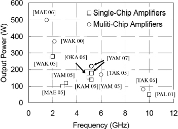
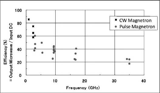
The characteristics of power versus frequency for microwave tubes and HPA using semiconductors are shown in Figure 3.2.
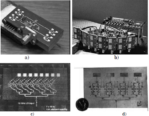
Figure 3.1. a) HPA circuit using semiconductors (GaAs FET); b) cooker-type magnetron (microwave tube) for MPT

Figure 3.2. Average RF output power versus frequency for various microwave tubes and semiconductors [TRE 02]

In the 1960s, microwave tubes were often used for MPT experiments because the efficiency of the microwave tube was higher than that of an HPA using semiconductors. Recently, the HPA using semiconductors is sometimes used for MPT experiments using a phased array because the efficiency of the HPA is now much improved. The microwave tube is still used for point-to-point or short-distance MPT experiments without any beam forming. The cooker-type magnetron in particular is still often used because of its low cost. We should choose the HPA using semiconductors or the microwave tube depending upon the purpose and system design. Frequency converters using semiconductors in inductive coupling and resonant coupling wireless power transfer (WPT) systems are always used. In particular, an inverter circuit is used at lower frequencies.
The rectifying circuit is another important system for WPT. Electrical products in house or in industry typically require 50/60 Hz AC or sometimes DC. Therefore, the WPT system must convert high frequencies in the kilohertz to gigahertz range to DC or 50/60 Hz AC. However, it is quite difficult to convert high frequencies to 50/60 Hz AC, and hence a rectifier that directly converts kilohertz to gigahertz to DC is always used in a WPT system. In the rectifier, semiconductor diodes are often used. In an MPT system, a receiving system consisting of an antenna and the rectifier is called a rectenna, i.e. a rectifying antenna.
3.2. Radio frequency (RF) generation – HPA using semiconductors
After the 1980s, semiconductor devices, especially transistors, played a leading role in the microwave world rather than microwave tubes. This change was brought about by advances in mobile phone networks. Semiconductor devices are expected to expand microwave applications, e.g. the phased array and active integrated antenna, because of their manageability and capacity for mass production. After the 1990s, some MPT experiments were conducted in Japan with phased arrays using semiconductor HPAs.
Typical transistor devices for microwave circuits are the field effect transistor (FET), the heterojunction bipolar transistor (HBT) and the high electron mobility transistor (HEMT). Present materials for semiconductor devices are Si for frequencies below a few gigahertz and GaAs for higher frequencies. Recently, GaN and SiC are expected to be applied to microwave circuits. GaN and SiC are designated as wide-band-gap semiconductors, which can accommodate high power and high frequencies similar to GaAs semiconductors. At microwave frequencies, GaN is typically used. SiC is used for the inverter circuit at lower frequencies. The characteristics of output power versus frequency for modern GaN HPAs are shown in Figure 3.3.
Figure 3.3. Characteristics of output power versus frequency for modern GaN HPAs
Microwave circuits are designed with these semiconductor devices. It is easy to control phase and amplitude via microwave circuits using semiconductor devices, e.g. amplifiers, phase shifters, modulators, etc. For microwave amplifiers, circuit design theoretically determines the efficiency and gain. Class A, B and C amplifiers are classified by the bias voltage used in the device. The amplifier circuit shown in Figure 3.4(a) is the same for class A, B and C amplifiers. These classes are also applied to kHz–MHz systems. The only difference is the operational point of V and I – bias voltage and the current, respectively – of a semiconductor. Theoretical amplifier efficiency is 50% for class A, 78.5% for class B and <100% for class C. In class B and C, efficiency is better than that in class A; however, the waveform is distorted and wave linearity cannot be maintained. For class C, the output power tends to be near zero when the efficiency is approximately 100%. As a result, class B and C devices are not typically used for wireless communication systems that require high wave linearity.
Figure 3.4. Class A, B and C amplifiers. a) Circuit, b) operation point for class A, c) operation point for class B and d) operation point for class C

Higher harmonics are effectively used to increase efficiency to levels that are theoretically 100% for class D, class E, class F and class inverse-F amplifiers operating at microwave frequencies. Class F [TYL 58, COL 99] and inverse-F [COL 99] amplifiers are especially expected to function as high-efficiency amplifiers for MPT systems. As shown in Figure 3.5, special impedance matching circuits controlling higher harmonics are added at the output and a transistor is driven at class B bias [HON 11]. The drain current becomes a half-wave-rectified waveform and higher harmonics occur at the class B bias circuit. The drain current Id (t) is transformed by the Fourier transform as follow1s:

where n = 2, 4, 6…
Figure 3.5. A class F/inverse-F amplifier [HON 11]
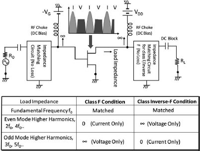
When the drain voltage Vd (t) consists of DC, the fundamental frequency f0, whose phase is 180° different from that of the fundamental frequency of the drain current, and odd harmonics, power consumption at the harmonics approaches zero and a power whose power factor is – 1 occurs at the fundamental frequency. This means that DC power is converted to f0 with theoretically 100% conversion efficiency if V1 is optimized by an impedance matching circuit for f0 and the bias voltage is adjusted. The relationships between equations [3.1] and [3.2] are shown in Figure 3.5.
The theoretical maximum efficiency and the number of harmonics of the current and voltage are presented in Table 3.1. It is important to increase the number of harmonics for higher efficiency. The theoretical efficiency of a class B amplifier is 78.5%. We should take care that an infinite number of even harmonics are required to realize a perfect half-wave-rectified waveform.
Table 3.1. Relationship between harmonics and efficiency [HON 11]

It is difficult to design the special impedance matching circuit with which we can control the higher harmonics. It is convenient to use distributed lines to design class F amplifiers, as shown in Figure 3.6. Some class F amplifiers have been developed for MPT applications. Figure 3.7 describes a class F amplifier operating at 1.9 GHz using GaN HEMT [ZHE 07]. The drain efficiency is 80.1% and power-added efficiency (PAE) = (Pout − Pin)/PDC) is a maximum of 72.6% at 1.9 GHz. The same group developed a class F amplifier operating at 5.65 GHz using AlGaN/GaN HEMT [KAM 11]. The drain efficiency is 90.7% and PAE is a maximum of 79.5% and the saturated power is 33.3 dBm.
Figure 3.6. Class F amplifier using distributed lines [HON 11]

Figure 3.7. Class F amplifier operating at 1.9 GHz using GaN HEMT developed by Univ. of Electro-Communications in Japan [ZHE 07]
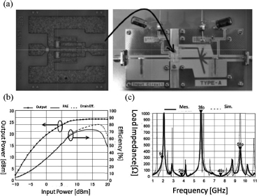
Figure 3.8. Class F amplifier operating at 5.65 GHz using AlGaN/GaN HEMT developed by Univ. of Electro-Communications in Japan [KAM 11]

The other requirement of semiconductor amplifiers for MPT use is amplifier linearity because the power level for MPT is much higher than for wireless communication systems. In addition, we have to suppress unexpected spurious radiation to reduce interference. The maximum efficiency is usually realized at a saturated bias voltage. It does not guarantee linearity between input and output microwaves, and nonlinearity causes high spurious radiation, which must be suppressed in MPT. Therefore, dissolution of tortuous relationships between efficiency and linearity is expected for MPT. This is one of the reasons why class F/inverse-F amplifiers are suitable for MPT applications because harmonics are used to increase the efficiency.
3.3. RF generation – microwave tubes
Several microwave generators or amplifiers are in use, such as magnetron, klystron and TWT/traveling wave tube amplifier (TWTA). Each microwave tube is typically used for cooking, plasma heating and satellite communications, respectively. Since the 1960s microwave tubes have been used for MPT.
3.3.1. Magnetrons
A magnetron is a crossed field tube in which E × B forces electrons emitted from a cathode to take a cyclonical path to an anode. It is a self-oscillatory device in which the anode contains a resonant RF structure. Figure 3.9 describes the structure of a magnetron and the principle of microwave generation in the magnetron. Efficiency of microwave generation in the magnetron is theoretically very high. High voltage is used and electrons, which flow in a vacuum, serve as the microwave source. The frequency is tuned only by the shape of a resonant cavity. The efficiencies of commercial magnetrons are shown in Figure 3.10.
Figure 3.9. Structure of the magnetron and the principle of microwave generation in a magnetron

Figure 3.10. Efficiency of a magnetron
The magnetron has a long history since its invention by A.W. Hull in 1921. The practical and efficient magnetron tube gathered world interest only after K. Okabe proposed the divided anode-type magnetron in 1928. Magnetron technologies were advanced during World War II, especially in the Japanese army. In 1945, P.L. Spencer of the Raytheon Company in the United States found that microwaves were emitted from the magnetron of a radar-melted chocolate in his pocket. Raytheon thus got a patent on the microwave oven and began producing ovens in 1952. After this, magnetrons were mainly produced for microwave ovens.
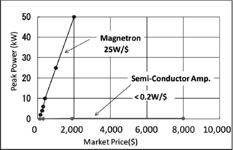
As a result, magnetrons in the 500–1,000 W range are widely used in microwave ovens operating at a frequency of 2.45 GHz, and it is a relatively inexpensive oscillator (less than $5). Magnetrons can be produced mainly using metal frames and magnets, and can therefore be produced at low cost. There is a net global capacity of 45.5 GW/year for all magnetrons used in microwave ovens, which have a yearly production of 50–55 million. The history of the magnetron is the same as that of the microwave oven. The first microwave oven using a magnetron sold in the United States shortly after World War II for more than $2,000, which is equivalent to approximately $20,000 today. In the 1960s, Japan played an important role in reducing the cost of the microwave oven. Compared with American manufactured tubes, which cost approximately $300 in the 1960s, the Japanese manufactured tubes cost less than $25. In 1970, U.S. manufacturers sold 40,000 ovens at $300–$400 a piece; however, by 1971, the Japanese had begun exporting low-cost models priced at $100–$200 less. Sales rapidly increased over the next 15 years, rising to approximately 1 million by 1975 and 10 million by 1985, nearly all of them manufactured by the Japanese. However, history repeats itself. Instead of Japanese microwave ovens, Korean- and Chinese-manufactured ovens presently are responsible for the reduction in the cost of the microwave ovens. Figure 3.11 shows a comparison of the market prices of semiconductor amplifiers and magnetrons in 2012. Magnetrons are overwhelmingly cheaper than semiconductor amplifiers.
Figure 3.11. Comparison of market price of semiconductors and magnetrons
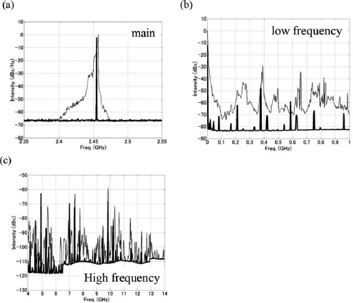
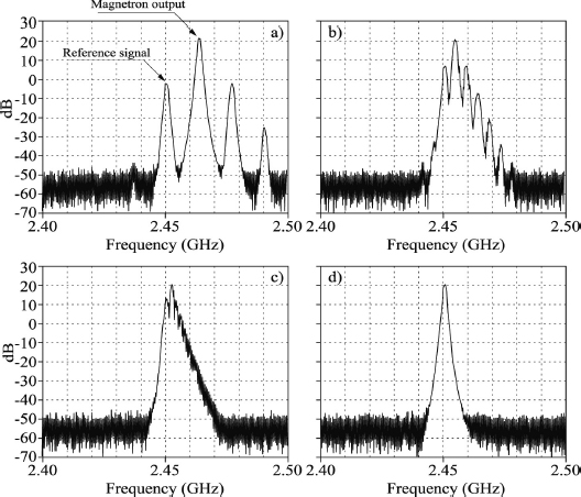
However, owing to our recent study, we know that the output microwave spectrum of the cooker-type magnetron depends on the stability of the DC power source and filament current [KAM 05]. If a stabilized DC power source is used for the magnetron and the filament current is deactivated after stable oscillation occurs, the spectrum, including low frequency and high frequency, is quiet, pure and adequate for its use in MPT (Figure 3.12). The Q factor of the magnetron with a stabilized DC power source is approximately 1.1 × 10⁵. Peak levels of higher harmonics are below −60 dBc, and other spurious radiation is below −100 dBc.
Figure 3.12. Output spectrum of a commonly used magnetron (bold: with a stabilized DC power supply and filament off, normal: with half-wave voltage doubler power supply and filament on). a) Main frequency; b) low frequency; c) high frequencyc
There remains, however, the problem of the frequency shift caused by magnetron heating and the impossibility of phase/frequency control even if the spurious radiation is suppressed. In the 1960s, Dr. Brown advanced the technologies used in magnetrons and developed a magnetron amplifier [BRO 81, BRO 89] whose frequency/phase was stabilized and controllable. For the magnetron amplifier, he adopted injection locking and a feedback loop to a magnetic field. Furthermore, he proposed the application of a magnetron amplifier to an MPT and solar power satellite (SPS).
Injection locking is accomplished by operating the magnetron as a reflection amplifier [SIV 94]. It can be used in a phased array using semiconductor microwave generators [YOR 98, STE 87]. The effect was formulated by R. Adler as Adler’s equation in equation [3.3] [ADL 46].
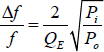
where Δf is the locking frequency width, which is basically the difference between the frequency of an injected weak signal and the output frequency of the oscillator, f is the frequency of the injected signal, QE is an external Q factor for the oscillator, in this case the magnetron, and Pi and Po are the input power for locking and the output power of the oscillator, respectively. Adler’s equation indicates that the frequency of the oscillator is locked to the frequency of the injected weak signal if Δf, which is decided by Adler’s equation, remains (see Figure 3.13). For example, an estimated Δf is shown in Figure 3.14. Experimental results for the injection locking of a magnetron are shown in Figure 3.15. As time passes, the frequency of the magnetron moves to the frequency of the injected signal. The bandwidth of the main frequency of the magnetron becomes narrower than that without injection locking.
Figure 3.13. A description of injection locking

Figure 3.14. Experimental result of the locking range Δf
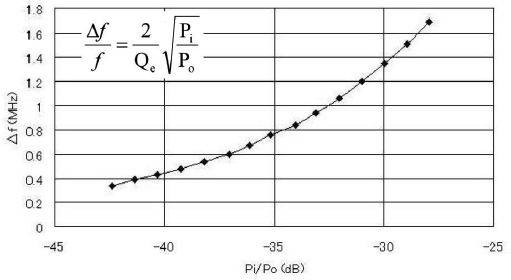
Figure 3.15. Experimental results of injection locking of a magnetron
Although the frequency can be locked and stabilized with the injection locking technique, the difference in phases remains even when the frequency is locked by injection locking. The difference in the phases θ between the injected signal and the oscillated signal is described by the following equation.
where Δf′ is the original difference in the frequency between the injected signal and the oscillated signal before injection locking. The experimental results showing the phase difference θ are given in Figure 3.16.
Figure 3.16. Experimental results of the phase difference θ

It is enough to use only one magnetron for MPT systems because the frequency of the magnetron is stabilized by injection locking. However, it is not enough to use two or more magnetrons for a phased array because the phases of the magnetrons are different. The frequency/phase of the magnetron can be controlled by the anode current (electric field E) or magnetic field B. Therefore, a phase-locked loop (PLL) feedback is used with injection locking in order to synchronize the phase of the reference signal and the microwave output. This is called the phase-controlled magnetron (PCM) developed by Kyoto University or a magnetron amplifier developed by Brown.
Kyoto University’s group has developed a PCM for MPT using different technologies from the one developed by Brown in the 1960s. For Kyoto University’s PCM, a PLL feedback to the anode current is adopted (Figure 3.13) [SHI 01]. A block diagram of the PCM is shown in Figure 3.17 and an image of the device is shown in Figure 3.18 [SHI 03]. However, a PLL feedback to a magnetic coil was adopted for the magnetron amplifier (Figure 3.19 and Figure 3.20) [BRO 89]. A phase and an amplitude control of the magnetron were proposed whose block diagram is shown in Figure 3.21 [BRO 81]. A phased array has been developed using PCMs by Kyoto University [SHI 03, SHI 00] (see section 3.4.4). Some research groups attempted to develop new magnetron systems in which they could control the phase of the microwave emitted from a cooker-type magnetron [HAT 98, HAT 99, CEL 97, SAN 00, TAH 05, TAH 06]. In these developed magnetrons, injection locking and a PLL feedback were adopted in the same manner as adopted in Brown’s work.
Figure 3.17. Phase-controlled magnetron system with an anode current feedback by Kyoto University [SHI 01]
Figure 3.18. Image of the phase-controlled magnetron [SHI 03]
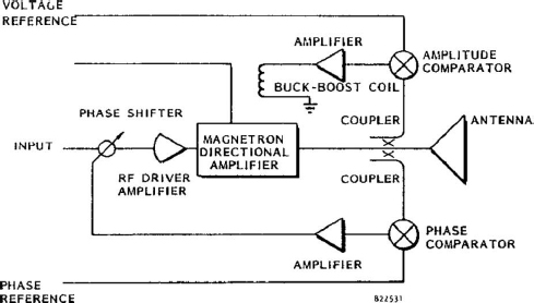
Figure 3.19. Circuit for phase-locked, high-gain magnetron directional amplifier by Brown [BRO 89]

Figure 3.20. Implementation of phase-locked, high-gain circuitry with addition of buckboost coil to microwave oven magnetron by Brown [BRO 89]

Figure 3.21. Phase- and amplitude-controlled magnetron system with magnetron amplifier by Brown [BRO 81]
PCMs can be used and have been used for phased arrays; however, some problems remain. One problem is a power loss of more than 10% in the circulator to inject the reference signal to the magnetron for injection locking. The other problem is the impossibility of power control while controlling the phase/frequency of the magnetron, which is theoretically due to the magnetron itself. To solve these two problems, a PLL magnetron and phase- and amplitude-controlled magnetron (PACM) have been developed by Kyoto University.
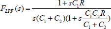
It is possible to stabilize the microwave of the magnetron by only using PLL feedback without injection locking. This is done by using a PLL magnetron. In the PLL magnetron, the magnetron and a DC power source are considered as voltage-controlled oscillators in normal PLL. A block diagram of the PLL magnetron is shown in Figure 3.22. Figure 3.23 is equivalent to the block diagram shown in Figure 3.22. An open-loop transfer function of the PLL magnetron can be estimated. The low pass filter (LPF) transfer function FLPF(s) is defined as follows:
The high-voltage source is considered as a first delay, which is defined as follows:
As a result, the open-loop transfer function FOPloop can be written as follows:
Figure 3.22. Diagram of the PLL magnetron

Figure 3.23. Block diagram for estimation of the open-loop transfer function

With equation [3.7], stability of the loop can be estimated with bode diagrams, as shown in Figure 3.24. The phase margin is approximately 40° and the feedback system is stable. Figure 3.25 shows the experimental results of phase and frequency locking of the PLL magnetron. The phase and frequency of the magnetron are stabilized and controlled by the PLL feedback loop only. The frequency stability is approximately 10−5 to 10−6. It is sufficient to control the microwave beam power, which has a lower stability than that of the PCM with injection locking.
Figure 3.24. Bode diagrams of PLL feedback shown in Figure 3.22

Figure 3.25. Experimental results of phase and frequency locking of the PLL magnetron

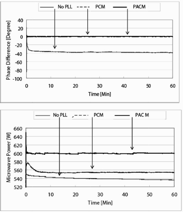
As mentioned above, the frequency/phase of the magnetron can be controlled by the anode current (electric field E) or magnetic field B. The problem is that the microwave power is simultaneously controlled by the anode current or the magnetic field. When we control and stabilize the frequency/phase of the magnetron by controlling the anode current, the microwave power is simultaneously controlled to unexpected levels. To solve this problem, a PACM with two feedback loops to the anode current and the magnetic field has been developed at Kyoto University. A block diagram of the PACM is shown in Figure 3.26. Figure 3.27 shows the results of amplitude control of the PACM. The amplitude of the microwave from the PACM is controlled from 300 to 500 W, with a stability of within 1% of the phase. Figure 3.28 shows the time dependence of the phase and the amplitude of the microwave from a magnetron, the PCM and the PACM. The frequency stability and error in phase and amplitude of the PACM are less than 10−6, within 1° and within 1%, respectively.
Figure 3.26. Block diagram of the PACM

Figure 3.27. Power control of the PACM

Figure 3.28. Time dependence of the phase and amplitude of the microwave from a magnetron, the PCM and the PACM
3.3.2. Traveling wave tube/traveling wave tube amplifier
TWT was invented by Kompfner during World War II and advanced theoretically and improved by Pierce and Field in 1945. The TWT is a linear beam tube with a helix structure. The helix slow wave structure (SWS) slows the RF waves down to just below the velocity of the electron beam. In the TWT, the interaction between the RF waves and the electron beam is continuous along the length of the SWS. The TWT can be used for an amplifier and is called a TWTA in that capacity. The longer the beam tube, the higher the gain. The applied frequency of the TWTA is very wide, ranging from 1 GHz band to the 60 GHz band. The typical output power of the TWT is a few hundred watts.
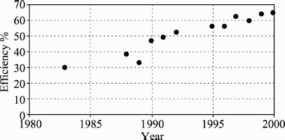
The TWTA is widely used in television broadcasting satellites and communication satellites. The TWTA has a proven track record in space. Before the 1980s, the efficiency of the TWTA was very low, approximately 30%. As such, this is not sufficient for use in an MPT system. There have been no MPT system designs or experiments using conventional TWTA. However, in recent years, a TWTA using a technique called velocity tapering energy recovery has been developed [GRA 99]. In this way, the net conversion rate has risen to approximately 70% [HEI 97] (Figure 3.29). The market for the TWTA has grown since 1972, and its cost has decreased [HEI 97]. Heider [HEI 97] identifies the main reasons for this price decrease as: (1) reduction in development time and effort due to standardization of the product, (2) reduction in parts cost due to higher volume purchase, (3) reduced manufacturing costs by manufacturing increased numbers of TWTAs in a shorter time frame and by more automatization in the manufacturing process and (4) reduction in test time and efforts due to the higher credibility of the product.
Figure 3.29. Trend of DC–RF conversion efficiency for TWTA [HEI 97]
Trends in the development of the TWT are microwave power module (MPM) and the phased array TWT. The MPM combines the best aspects of TWT, semiconductor amplifiers and state-of-the-art power supply technology into one package. This makes MPM a good candidate for space applications because it has high conversion efficiency, small size and low weight. In the near future, MPT systems using TWTA could be considered.
The TWTA is normally used as one transmitter. However, a phased array using TWTAs are tested for broadcasting satellite systems [YAM 07b]. TWTA array is used as a feed array of a parabolic antenna. For the phased array, low power TWTA is required. Mini-TWTA is developed for the phased array and its power, gain and efficiency are 10.8 W, 36.3 dB and 46.2% at 21.4–22 GHz, respectively.
Figure 3.30. Phased array using TWTAs [YAM 07b]
3.3.3. Klystron
The klystron was invented by the Varian brothers in the late 1930s. A klystron is also a linear beam tube containing cavities. Electrons are emitted from the cathode and an electron beam passes through the cavities. When the RF is input from the input cavity, the electron beam is modulated and the RF input is amplified. A klystron is an HPA from tens of kilowatts to a few megawatts with high efficiency of more than 70%. However, it requires a strong power supply and a heavy magnet. Klystrons are used for broadcast applications in the 400–850 MHz band. They are also used for uplinks (earth stations beaming to orbital satellites). The other application of the klystron is in fusion.
The klystron was used in an MPT demonstration in 1975 at the JPL Goldstone Facility. One klystron transmitted a microwave of 450 kW at an operating frequency of 2.388 GHz. The klystron is suitable for large MPT systems such as SPS. The SPS designed by NASA/DOE in 1980 was designed with a phased array consisting of klystrons. However, no klystron phased array system has yet been constructed.
3.4 Beam-forming and target-detecting technologies with phased array
3.4.1. Introduction
We know that beam direction can be controlled in the phased array. However, the compatibility of high-efficiency beam forming of MPT is very difficult. In Japan, some trials of MPT experiments with a phased array were carried out in the 1990s and in the 21st Century. Phased array with semiconductors for the MPT in Japan are described, which were developed for the microwave lifted airplane experiment (MILAX) and the International Space Year – Microwave Energy Transmission in Space (ISY-METS) experiment in 1990s, and JAXA’s SPS demonstrator, USEF/METI’s active integrated antenna (AIA) system and corporative works with Mitsubishi Electric Cooperation and Kyoto University. Magnetron phased arrays, which were developed in Kyoto University, are also developed in Japan. Retrodirective, a target detection technique using radiowaves, is important for beam forming. The Japanese trials using a phased array and a retrodirective target-detecting system are described in this section. This section is based on [SHI 13C].
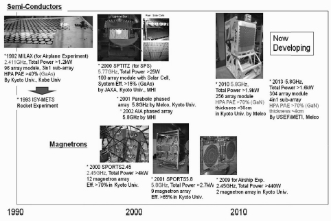
Each project of the phased array is independent. In each project, they had a research target, for example, to fly a fuel-free airplane with microwaves, to develop the thickest phased array or to develop a magnetron phased array itself. But they are based on the previous project to develop new phased array. The trend of the development of the phased array is shown in Figure 3.31. Key words are “higher frequency”, “higher efficiency” and “thick size and lightweight”. In each project, they adopted the newest technologies to develop the phased array.
Figure 3.31. Historical summary of phased array for MPT [SHI 13]
3.4.2. Phased array in the 1990s
In 1983, Kyoto University’s group in Japan carried out the first successful MPT rocket experiment called the microwave ionosphere nonlinear interaction experiment (MINIX). The experiment yielded new plasma data and theory about the nonlinear interaction between high-power microwave beams and ionospheric plasmas [MAT 86, KAY 86, NAG 86]. A cooker-type magnetron and waveguide antenna was used to transmit the 2.45 GHz microwave power from the mother transmitter rocket to the daughter receiver rocket in MINIX. Ten years later, they planned the next rocket MPT experiment with a phased array to describe detailed plasma physics. Data about the angle between the magnetic field and excited plasma wave were required to calculate the level of the excited plasma wave, which is caused by the high-power microwave beam. They also had to concentrate the microwave power to a narrow area to estimate the angle between a magnetic field and excited plasma wave. Therefore, the phased array was suitable to control the microwave beam direction and to calculate the angle between a magnetic field and excited plasma wave. The magnetic field could be measured in the rocket experiment. The microwave beam direction was estimated by the beam control data, together with the experimental data about beam direction collected before the rocket experiment. The second rocket MPT experiment with a phased array was called the ISY-METS by Kyoto University, Kobe University, Texas A&M University from USA, Communication Research Laboratory (CRL) (presently known as the National Institute of Information and Communications Technology (NICT)) and the Institute of Space and Astronautical Science (ISAS).
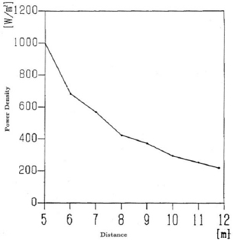
Before the ISY-METS experiment, the fuel-free airplane experiment called the MILAX was carried out in August 1992 [MAT 93]. The phased array developed for ISY-METS was used to transmit the microwave power. In total, 96 GaAs semiconductor amplifiers and 4-bit digital phase shifters were connected to 288 antenna elements at 2.411 GHz. This meant that there were three antennas in one amplifier subarray (Figure 3.32). The diameter of the phased array was approximately 1.3 m. The measured beam pattern is shown in Figure 3.33. The beam width was approximately 6°. The gain of the amplifier was 42 dB at 0 dBm input. Output power was approximately 42 dBm (Figure 3.34). The PAE of the amplifier was approximately 40%. The total microwave power was 1.25 kW and consisted of a continuous wave (CW) with no modulation. The measured power density is shown in Figure 3.35.
Figure 3.32. First phased array for MPT in MILAX in 1992
Figure 3.33. Beam pattern of the MILAX phased array

Figure 3.34. Measured output power, efficiency and gain of the GaAs amplifiers in MILAX and ISY-METS

Figure 3.35. Transmitted power density at different distance
The phased array was assembled on the roof of a car. The car drove under the fuel-free airplane as much as possible and the microwave was controlled toward the fuel-free model airplane using a computer and data from two charged coupled device (CCD) cameras, which detected the position of the target. One of the CCD cameras is shown on the right-hand side of Figure 3.32. The rectenna array on the airplane’s body is shown in Figure 3.36. There were in total 120 rectennas. The element spacing was 0.7λ. The efficiency of the rectenna was approximately 61% at 1 W output DC power. The airplane flew freely using only the microwave power that was fed by the phased array. The airplane flew at approximately 10 m above ground level. The maximum obtained DC power from the rectenna array was approximately 88 W and was sufficient to fly the airplane. This was the first MPT field experiment using a phased array in the world.
Figure 3.36. MILAX airplane and rectenna array

After the success of MILAX, the rocket experiment with a phased array called ISY-METS was carried out in February 1993 [KAY 93]. The phased array was arranged to cross plane and folded into the head cone of the rocket (Figure 3.37). There were (2 × 8 = 16) antennas fitted to each of the four panels. They used the same GaAs semiconductor amplifiers and 4-bit digital phase shifters. Figure 3.38 shows the measured beam pattern that is concentrated on one point, 10 m away from the antenna, and there was no other documented condition to measure the beam pattern [KAY 93]. Thus, we should consider the vertical axis as relative power only. The large side lobe was achieved by the positioning of the antennas. Figure 3.39 shows the concentrated power received by a dipole antenna at different distances from the transmitting antenna by a solid line, while circles indicate the flight data [AKI 93]. They succeeded in the beam control in space from the phased array in the mother rocket to a receiver in the daughter rocket.
Figure 3.37. Phased array in ISY-METS rocket experiment. a) Expanded shape for experiment; b) folded shape in launch
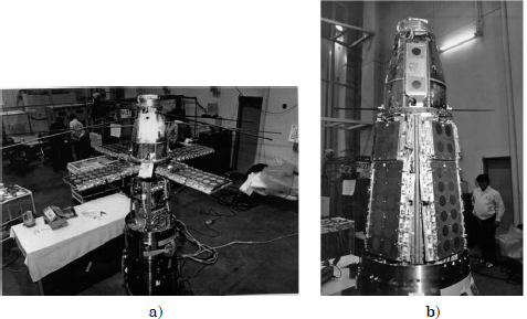
Figure 3.38. Beam pattern of the ISY-METS phased array

Figure 3.39. Received power by a dipole antenna at different distances

3.4.3. Phased array in the 2000s
The phased arrays in MILAX and ISY-METS were insufficient for power transfer. Recently, the phased array technology itself advanced into synthetic aperture radar (SAR). The related technology of adaptive arrays advanced into multiple input multiple output (MIMO) systems. However, MPT requires higher efficiency in the phased array.
In the 2000s in Japan, some trials were carried out as part of the development of high-efficiency phased arrays, mainly for SPS applications. One of the projects was SPRITZ in FY2000 (Figure 3.40) [MAT 02a]. The characteristics of the SPRITZ are as follows:
Figure 3.40. SPRITZ in FY2000 – phased array for the SPS

Total system efficiency of the phased array was 15%, which is without solar cells and that includes losses in the feeder network and a phase shifter. The efficiency was not enough; however, this was the first trial of the sandwich-type phased array, which was composed of rear solar cells and a front phased array. Theoretical and measured beam patterns are shown in Figure 3.41. The beam width was 7.3°. The antenna gain was 17.6 dBi and the equivalent isotropic radiated power (EIRP) was 58 dBm. A rectenna with 51.2% efficiency received the microwave power and lighted an LED to detect the microwave beam.
Figure 3.41. Theoretical and measured beam pattern of SPRITZ phased array

High efficiency is important in the phased array for MPT. Some new ideas to increase the efficiency or to decrease the loss against the development of high-efficiency microwave circuits were required. In FY2001, Kyoto University and Mistubishi Electric Corporation developed a parabolic antenna phased array at 5.8 GHz to retain high efficiency of the microwave circuits (Figure 3.42). The loss is evident in all amplifiers (except in microwave HPAs), for example driver amplifiers, phase shifter and beam control circuits, isolators or occurrence of grating lobes. Therefore, to decrease the power loss, a parabolic antenna phased array with the following ideas was developed [IKE 02, MIK 04].
Figure 3.42. Parabolic phased array with DDS/PLL oscillators. a) System block diagram; b) image
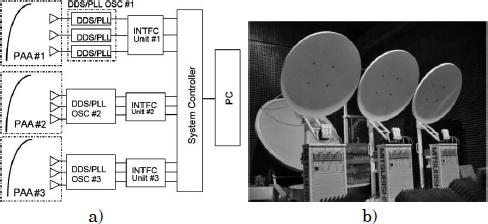
One DDS/PLL oscillator generates more than 8 W of continuous microwave power. Three DDS/PLLs are used in one parabolic antenna and the phased array is composed of three parabolic antennas, thus the total radiated power is more than 72 W (8 W × 3 W × 3 W). Diameter and gain of the reflector are 1.2 m and 32.2 dB, respectively. The controllable beam direction is within 5° on the horizontal line. Parabolic antenna spacing is 1.25 m. Theoretical and measured beam patterns at the Fresnel region (7 m away from the baseline) are shown in Figure 3.43. We can control the beam direction by suppressing grating lobes with the parabolic antenna phased array.
USEF SPS Study Team in Japan developed some types of phased array for SPS. In FY2002, the USEF SPS Study Team and Mitsubishi Heavy Industry developed a phased array whose characteristics were as follows [KIM 04]:
Figure 3.43. Theoretical and measured beam pattern of parabolic antenna phased array at Fresnel region
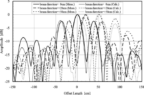
Figure 3.44. Measured output power, efficiency and gain of the GaAs amplifiers in AIA developed by USEF SPS Study Team

The phased array was composed of three layers with receiving, phase-shifting, and transmitting parts as an AIA (Figure 3.45). The microwave source was fed from the backside of the AIA through the air and the received microwave was amplified and controlled through the phase-shifting and transmitting parts. The array was approximately 360 mm × 360 mm × 70 mm and the antenna gain was 10.8 dBi. The total weight was approximately 11 kg. The radiation efficiency of transmission antennas was more than 90% in approximately 37° range of beam width (Figure 4.46). The measurement result of the beam pattern is shown in Figure 4.47, when the microwave beam was controlled in the horizontal directions.
Figure 3.45. Active integrated antenna for MPT in FY2002. a) Front; b) back

Figure 3.46. Radiation efficiency versus beam width
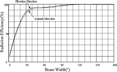
Figure 3.47. Measured beam pattern of USEF-AIA

USEF continued to develop a high-efficiency phased array for SPS. The basic plan for space policy was established by the Strategic Headquarters for Space Policy in June 2009. This basic plan for space policy that was forged at this time was based on the Basic Space Law established in May 2008 and is the Japan’s first basic policy relating to space activities. In the plan, SPS was selected based on nine systems and programs for the use and R&D of space [BAS 08a, BAS 08b].
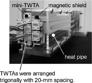
Based on this, a high-efficiency and thin phased array development project, which is supported by METI, started in FY2009 [FUS 11]. The author is a chair person of this project and Mitsubishi Electric Corporation is developing the phased array. The target of the phased array is: (1) 5.8 GHz CW, no modulation, (2) >70% PAE GaN semiconductor MMIC amplifier (Figure 3.48), (3) MMIC 5-bit phase shifters, (4) <40 mm thick phased array (Figure 3.49), (5) 120 cm × 120 cm array, (6) 76 amplifier/phase shifter modules on each panel of a four-panel system (76 × 4 = 304 modules in system), (7) four antenna – one module subarray and (8) total power > 1.6 kW CW.
Figure 3.48. Metal packaged GaN HEMT amplifier [HOM 11]

Figure 3.49. Structure image of sub-array [HOM 11]

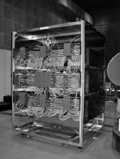
At the end of FY2010, a new phased array was installed in Kyoto University as multipurpose research equipment (Figure 3.50) [HOM 11, YAM 10]. The characteristics of the phased array in Kyoto University are as follows:
Figure 3.50. New phased array for MPT with GaN FET and class F amplifier circuits developed in Kyoto University and by Mitsubishi Electric Cooperation in FY2010
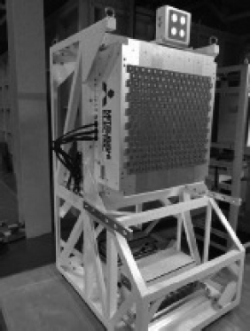
Figure 3.51. Measured output power, efficiency and gain of the GaN amplifiers in phased array in Kyoto University

The phased array system consists of phased array equipment, beam control units and a cooling unit. The beam control units consist of an antenna control unit, a PC and the retrodirective equipment. The rectenna array system consists of the rectenna array, a DC/DC converter, a load and the retrodirective equipment. Figure 3.52 shows a simulated beam pattern, and Figure 3.53 shows measured beam patterns, when the main beam is steered to EL = −15°, −10°, −5°, 0°, 5°,10°, 15°. In each beam steering angle, the obtained steering accuracy was within 0.1°. The phased array is open for use by inter-universities and international collaborative studies.
Figure 3.52. Simulated beam pattern of the phased array in Kyoto University

Figure 3.53. Measured elevation beam pattern of phased array (beam steering angle: EL= −15 °, −5°, 0°, 5°, 15° (AZ = 0°))

3.4.4. Phased array using magnetrons
The compatibility of high-efficiency beam forming of MPT with semiconductor technology has not yet been realized. We at Kyoto University proposed and developed a new phased array with magnetrons. The efficiency of the magnetron is more than 70%, and it is the cheapest available microwave device. We cannot control the phase of the magnetron itself because it is a high-power generator. However, we developed a PCM with an injection-locking technique and a PLL feedback to a voltage source of the magnetron [SHI 03]. The original idea of PCM was given by Brown [BRO 88]. We revised the PCM and developed a phased array with PCM at 2.45 GHz in FY2000 and at 5.8 GHz in FY2001, which are called the Space Power Radio Transmission System for 2.45 GHz (SPORTS-2.45) and Space Power Radio Transmission System for 5.8 GHz (SPORTS-5.8), respectively [SHI 04b].
Characteristics of the SPORTS-2.45 are as follows:
In SPORTS-2.45, we always turn off the filament current during power transmitting after stable oscillation occurs because filament current causes noise in the magnetron. We cannot turn off the filament current in the cooker-type magnetron because a half-wave rectification voltage source is used for the microwave oven. The current heats the filament and the heat from the filament current usually supports electron emission to generate a microwave. Thus, enough electrons cannot be provided in the cooker-type magnetron with a half-wave rectification voltage source without any filament current. However, when we use a stabilized DC current source with the same cooker-type magnetron, the filament is heated enough without the filament current because the stabilized DC current obstructs the cooling of the filament. We achieved better than 10−8 frequency stability, relative to the frequency stability of an input reference signal with the stabilized DC power source and without the filament current.
We can select from two types of antenna in SPORTS-2.45 (Figure 3.54). One is a 12-horn antenna array with low power loss but with a limited narrow beam scanning capability. The size and gain of each horn antenna are 192 mm × 142 mm and 17.73 dBi, respectively. System efficiency of the horn array is high, but large side lobes and grating lobes appear when we change the beam direction. The simulated beam pattern in front direction is shown in Figure 3.55. When we change the beam direction to wide range, grating lobes arise.
Figure 3.54. SPORTS-2.45 magnetron phased array; a) 12 phase controlled magnetrons, b) horn antenna array that is directly connected to the PCMs, c) antennas connected to PCMs through 1-bit subphase shifters after eight-way power dividers

Figure 3.55. Simulated beam pattern of 12-horn antenna array

The other is a 96-dipole antenna array with power dividers and 1-bit subphase shifters. Element spacing is 0.7λ. To expand the beam control area without large side lobes and grating lobes, we should shorten element spacing. But the power of the PCM is too large to connect a small dipole. Thus, we should divide the power from the PCM to provide the small dipole. This is the concept of a subarray. The normal subarray makes a grating lobe that diffuses the microwave power except for the target when we change the beam direction. Therefore, we proposed a 1-bit subphase shifter that is installed after a power divider to suppress the grating lobe. Loss in the digital phase shifter is commonly estimated as 1 dB/1 bit. Thus, the loss of the 1-bit subphase shifter is smaller than that of the 4- or 5-bit phase shifters. If we do not use any subphase shifters, then the loss is the same as a subarray system and large side lobes and grating lobes appear. However, we can suppress the grating lobes with the subphase shifter system and can retain high efficiency of the phased array [SHI 04].
Characteristics of the SPORTS-5.8 are as follows:
In SPORTS-5.8, we only adopt a subarray with power dividers after the 5.8 GHz PCMs without any subphase shifters (Figure 3.56). The power loss after output of PCM is less than 1.5 dB. Matsushita Co. developed the 5.8 GHz magnetron. We always turn off the filament current during power transmitting after the stable oscillation occurs.
Figure 3.56. SPORTS-5.8 magnetron phased array
In 2009, Kyoto University succeeded in a field MPT experiment using PCM technology. We transmitted 2.46 GHz microwave power with two 110 W output power PCMs from an airship to the ground [MIT 10]. Two radial slot antennas were used in the experiment, whose diameter was 72 cm, with a gain and aperture efficiency of 22.7 dBi and 54.6%, respectively. Element spacing was 116 cm (Figure 3.57). Theoretical and measured beam patterns are shown in Figures 3.58 and 3.59, respectively. Characteristics of this magnetron phased array are as follows:
Figure 3.57. Radial slot antenna array with two PCMs for MPT airship experiment in 2009 in Japan

Figure 3.58. Theoretical beam pattern of two radial slot antenna arrays. For a color version of this figure, see www.iste.co.uk/shinohara/radiowaves.zip

Figure 3.59. Measured beam pattern (E-field) oftwo radial slot antenna arrays at 50 m distance. Radiated microwave power is 600 W

In Kyoto University and Kyushu Technical University, we also apply the PCM phased array for MPT to a Mars observation airplane [NAG 11a]. We consider the magnetron phased array as one of the solutions for a high-efficiency phased array system.
3.4.5. Retrodirective system
Target detection is important for the phased array system because of accurate and high-efficiency microwave power transfer. Retrodirective target detection, in which a pilot signal is used both for the target detection and for detecting antenna positioning, is often used for the MPT system. An extensive research is being conducted on retrodirective array research for wireless communications in the world [MIY 02]. The developed retrodirective systems for various objectives are shown in Figure 3.60. [QUB, DID 98, QIA 98, MIY 01].
Figure 3.60. Various retrodirective arrays with phase conjugate circuits developed in a) Queen’s University (62–66 GHz)[HTT], b) Jet Propulsion Laboratory and University of Michigan in 2001 (5.9 GHz)[DlD 98], c) UCLA in 1995 (6 GHz)[QlA 98], and d) UCLA in 2000 (6 GHz)[MIY 01]
In Japan, some types of retrodirective system were developed after the 1980s. In 1987, Kyoto University and Mitsubishi Electric Corporation developed a retrodirective system with two asymmetric pilot signals (Figure 3.61) [MAT 02b]. We use the same frequency for the pilot signal and the transmitting microwave in the conventional retrodirective system. Therefore, interference between the pilot signal and the transmitting microwave may occur. Therefore, they proposed two asymmetric pilot signal systems with ωt + Δω and ωt +2Δω. Seven antennas were used for receiving two pilot signals as well as for microwave power transfer. The microwave frequency was 2.45 GHz.
Figure 3.61. Retrodirective system with two asymmetric pilot signals developed by Kyoto University and Mitsubishi Electric Corporation. a) Image of the phased array. b) Block diagram of retrodirective system with two asymmetric pilot signals

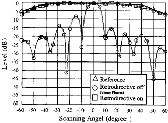
In 1996, Kyoto University and Nissan Motor Company (presently IHI Aerospace) developed another retrodirective system. To suppress interference between the pilot signal and the transmitting microwave, they proposed to use a one-third frequency pilot signal (817 MHz) (Figure 3.62) [MAT 02a]. Transmitting microwave frequency was at 2.45 GHz. Eight transmitting antennas were put in one-dimensional line. On both sides of the transmitting antennas, pilot signal receiving antennas were placed. When we consider only a onedimensional horizontal line, each pilot signal receiving antenna corresponds to a transmitting antenna. It did not contain a local oscillator to reduce unmatched frequency between a pilot signal and the local oscillator. Figure 3.63 shows the measured beam pattern of this retrodirective system. When there is no retrodirective target detected, the data indicate the array pattern itself. When the retrodirective system is on, the microwave beam chases the pilot signal source and the data indicate the element pattern.
Figure 3.62. Retrodirective system with 1/3 frequency pilot signal developed by Kyoto University and Nissan Motor Company. a) Image of the phased array. b) Block diagram of retrodirective system with 1/3 frequency pilot signal
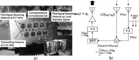
Figure 3.63. Measured beam pattern of retrodirective system in on and off state
In FY2003, the USEF SPS Study Team together with Mistubishi Electric Corporation developed a PLL-heterodyne retrodirective system [MIZ 04]. Microwave frequency was 5.77 GHz and the pilot signal frequency was 3.884 GHz. There were eight transmitting antennas (the other antennas in Figure 3.64 are dummies). Beam patterns are shown in Figures 3.65(a)–(c).
Figure 3.64. PLL-heterodyne retrodirective system developed by Mitsubishi Electric Corporation with USEF SPS Study Team in FY2003 [MAT 02b]. a) lmage and b) block diagram of conventional retrodirective. c) Block diagram of PLL-heterodyne retrodirective

Figure 3.65. Beam pattern of PLL-heterodyne retrodirective system [MAT 02b]. a) Beam target: 0°. b) Beam target: 25°. c) Beam pattern with and without retrodirective
In January 2006, Kobe University, ISAS and ESA’s research group succeeded in a retrodirective MPT experiment from a rocket to the ground [NAK 05, KAY 06]. They opened the antenna and structure on the rocket and transmitted microwaves to the pilot signal target.
3.5. RF rectifier – rectenna and tube type
3.5.1. General rectifying theory of rectenna
A rectenna is a passive element with rectifying diodes that operates without an internal power source. It can receive microwave power and rectify it to produce DC power. A general block diagram of a rectenna is shown in Figure 3.66. A low-pass filter is installed between the antenna and the rectifying circuit to suppress reradiation of higher harmonics from the diodes. An output filter is used not only to stabilize the DC current, but also to increase RF–DC conversion efficiency.
Figure 3.66. General block diagram of a rectenna

We can apply various antennas and rectifying circuits. Their selection depends on the requirements for a wireless power system and its users. When we use a rectenna array, its antennas are capable of absorbing 100% of the input microwaves [DIA 68, STA 74, ITO 86]. Higher efficiency rectifying circuits are required because a WPT system is an energy system. There are various rectifying circuits that can theoretically reach 100% efficiency. The details of general rectifying circuits are described in [SAE 11] and [OHI 13].
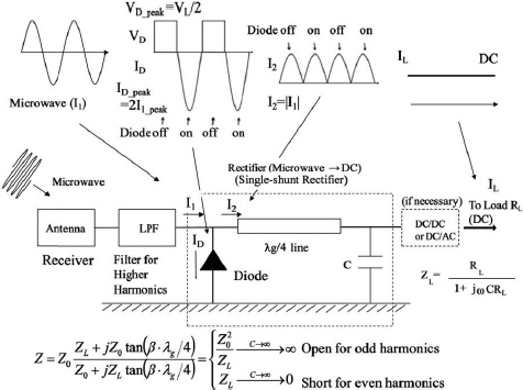
In MPT, a single-shunt full-wave rectifier is often used. The single-shunt rectifier is composed of a diode and a capacitor connected in parallel to a λg/4 distributed line. λg is the effective wavelength of an input radiowave (microwave or millimeter wave). The λg/4 distributed line and the parallel capacitance work in tandem as an output filter. The single-shunt rectifier can theoretically rectify microwave input at 100% efficiency with only one diode because of the enhancing effect of the output filter [GUT 79].
Figure 3.67 shows the block diagram of a rectenna with a single-shunt rectifier and its theoretical output waveform along with its analysis. A low-pass filter and a capacitance for DC conversion are usually installed between an antenna and a rectifier. An input impedance Z to the right of the diode is formulated as follows:
where RL is the load resistance, C is the capacitance of the output filter, Z0 is the characteristic impedance of a distributed line and its circuit, l is the length of the distributed line, β is a phase constant ![]() and ω is the angular frequency of the input electromagnetic wave. For odd harmonics, 3ω, 5ω, …, tanωl and Z become infinity; when l = λg/4 and C is large enough, then
and ω is the angular frequency of the input electromagnetic wave. For odd harmonics, 3ω, 5ω, …, tanωl and Z become infinity; when l = λg/4 and C is large enough, then ![]() . For even harmonics, 2ω, 4ω, …, tanβl and Z become zero; when l = λg/4 and C is large enough, then Z = ZL. These are the most important concepts regarding the theory of the single-shunt rectifier [GUT 79].
. For even harmonics, 2ω, 4ω, …, tanβl and Z become zero; when l = λg/4 and C is large enough, then Z = ZL. These are the most important concepts regarding the theory of the single-shunt rectifier [GUT 79].
Figure 3.67. Block diagram of a rectenna with a single-shunt full-wave rectifier and its theoretical waveform
I1(t) is the input current through the LPF, defined as follows:
where t is the time and I0 is the amplitude of the current of an input electromagnetic wave. In WPT theory, we usually assume a pure, continuous and unmodulated wave.
When the diode is open at 0 < ωt < π, I2 flows to the right-hand side of the diode, and ID is the diode current. These currents are defined as follows:
As previously discussed, I2 must be composed of even harmonics to obtain the efficiency enhancement effect of the output filter. As a result, I2 must be a function with a cycle of π described as follows:
When the diode is short at π < ωt < 2π, then I2 and ID are:
As a result, I2 becomes a full-wave waveform described as follows:
In the diode, the waveform becomes a half-wave doubler. Thus, the behavior of the single-shunt rectifier is very similar to that of a class F amplifier.
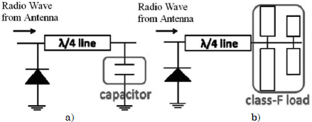
The class F rectenna, which is not the single-shunt rectenna, was originally proposed by Kyoto University (Figure 3.68) [HAT 13]. A second group developed a class F rectenna with 77.9% efficiency at 2.45 GHz [NOD 12b]; theoretical analysis of the class F rectenna is described in [GUO 13]. Class C, class E and class inverse-F rectennas have also been proposed and developed [ROB 12, RUI 12]. In these reports, the RF–DC conversion efficiencies of class C, class E and class inverse-F rectennas were 72.8% at 2.45 GHz, 83% at 950 MHz with HEMT diodes and 85% at 2.14 GHz with GaN HEMT diodes, respectively.
Many rectennas using a single-shunt rectifier have demonstrated 70–80% RF–DC conversion efficiency [SHI 12]. Compared to a four-diode bridge rectifier, the efficiency of the single-shunt rectifier is higher because there is only one diode with a resistance loss factor in the single-shunt rectifier.
Figure 3.68. Concept of class F load rectenna; a) normal single shunt, b) proposed class F load type
Theoretically, the RF–DC conversion efficiency of a rectenna is 100%. But a real diode and a real circuit introduce loss factors. The V-I characteristics of the diode, in particular, determine the RF–DC conversion efficiency [YOO 92, MCS 98]. Figure 3.69 shows typical RF–DC conversion efficiencies of rectennas, showing not only single shunt, but also all rectifying circuits with diodes. VJ is the junction voltage of a diode and Vbr is the breakdown voltage of a diode, and their characteristic curves are shown in Figure 3.70. These characteristics also hold for a connected load instead of the input power.
Figure 3.69. Typical relationships between RF–DC conversion efficiency and input power [YOO 92]

Figure 3.70. Rectification cycle represented by an input fundamental waveform and diode junction voltage waveforms impressed on the diode V-I curve [MAC 98]

The waveform at a diode can be expressed as:

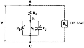
where Vo is the output self-bias DC voltage across the load and V1 is the peak voltage amplitude of the input microwave. Vd0 and Vd1 are the DC and fundamental frequency components of the diode junction voltage and Vbi is the diode’s built-in voltage in the forward bias region. The diode model consists of a series resistance Rs, a nonlinear junction resistance Rj described by its DC I-V characteristics and a nonlinear junction capacitance Cj as shown in Figure 3.71 [YOO 92, MCS 98]. A DC load resistance RL is connected in parallel to the diode along a DC path represented by the dotted line to complete the DC circuit. The junction resistance is assumed to be zero for forward bias and infinite for reverse bias. By applying Kirchoff’s voltage law, closed-form equations for the diode’s efficiency and input impedance are determined. The RF–DC conversion efficiency η. is theoretically calculated from equation [3.20] [YOO 92, MCS 98]:

θon is defined as follows:
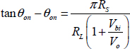
Cj is a nonlinear junction capacitance and is described with zero bias junction capacitance Cj0 as follows:
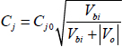
Figure 3.71. Equivalent circuit of a diode [YOO 92]
The estimated RF–DC conversion efficiency of a diode calculated using equations [3.20]–[3.22] for various circuit parameters is shown in Figure 3.72.
Figure 3.72. RF–DC conversion efficiency of a diode estimated by frequency, internal resistance and capacitance (r = Rs/RL) [MAC 98] (point A: Rs = 0.5 Ω, Cj0 = 3 pf, 2.45 GHz, RL = 100 Ω; point B: Rs = 4.85 Ω, Cj0 = 0.13 pf, 35 GHz, RL = 100 Ω) [YOO 92]

3.5.2. Various rectennas I – rectifying circuits
The single shunt is not the only rectifying circuit available. Various rectennas have been proposed. The world’s first rectenna developed by Brown in 1963 was a normal bridged rectifier (Figure 3.73) [BRO 80]. The operating frequency was 2.45 GHz. The frequency of 2.45 GHz (and 5.8 GHz) lies in the industrial, scientific and medical (ISM) band. The rectenna was a string-type rectenna developed for a fuel-free helicopter experiment in 1964. It was conceived at Raytheon Co., and a power output of 7 W was produced at approximately 40% efficiency with four point-contact diodes.
Figure 3.73. World’s first rectenna developed by Brown [BRO 80]

Next, Brown developed the first single-shunt rectenna (Figure 3.74) [BRO 78]. It was developed for low-cost production. The same type of rectenna was adopted for a 1.6 mile MPT field experiment in Goldstone in 1975 [BRO 84]. Brown developed a large rectenna array with a size of 3.4 m × 7.2 m. The transmitted microwave power from the klystron source was 450 kW at a frequency of 2.388 GHz in the field experiment, and the achieved rectified DC power was 30 kW DC with 82.5% rectifying efficiency. At last, Brown achieved 90% efficiency of the rectenna at 2.45 GHz (Figure 3.75) [BRO 76]. In parallel, Brown also developed a thin rectenna shown in Figure 3.76 [BRO 82].
Figure 3.74. Single-shunt rectenna developed by Brown [BRO 78]

Figure 3.75. Progress in optimized efficiency of rectenna by Brown [BRO 76]
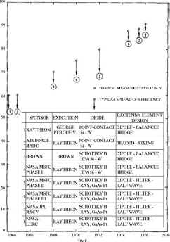
Figure 3.76. Thin rectenna developed by Brown [BRO 82]

After the progress of the rectenna achieved by Brown, some interesting approaches were considered to increase the efficiency. Figure 3.77 shows a full-wave rectifier with 0°– 180° combination through an antenna [ITO 93]. In that rectifier, a combination of reverse phase microwave was used to realize full-wave rectifying. The antenna plays an important role in creating the reverse phase. The other approach using a 0°–180° combination had a rat-race hybrid circuit (Figure 3.78) [KOB 93]. The frequency was 2.45 GHz in both rectennas discussed in [ITO 93] and [KOB 93].
Figure 3.77. Full-wave rectifier with 0°–180° combination through the antenna [ITO 93]

Figure 3.78. Full-wave rectifier with 0°–180° combination through a rat-race hybrid (originally in Japanese) [KOB 93]
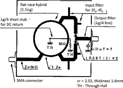
A diode used in a rectifying circuit is a nonlinear device. Therefore, we cannot match its impedance to suppress reflection from the rectifying circuit with varying microwave input or connected load. When the optimum input microwave is input and the optimum load is connected to the rectifying circuit, the reflected microwave signal is less than 1%, but RF-DC the conversion efficiency becomes less than 10% and the reflected microwave signal is more than 50% when the input microwave and the connected load are not optimal (see Figure 3.69). Thus a rectenna with utilization of the reflected microwave was proposed by Kyoto University [KIM 02, KIM 03]. Three types of rectennas, called “feedback rectennas”, were proposed and developed (Figure 3.79(a)), “feedback rectenna with rat-race hybrid” (Figure 3.79(b)) and “rectenna with direct utilization of reflected microwave” (Figure 3.79(c)), all operating at 2.45 GHz.
All rectennas in this chapter have diodes to rectify microwaves. But Professor Popovic’s group adopted an FET to rectify microwaves. She proposed and developed a rectenna with FET, which is the same as a class inverse-F amplifier (Figure 3.80) [ROB 12]. Any amplifier will function as a rectifier, and at microwave frequencies as a self-synchronous rectifier without any gate drive Professor Popovic called this “PA-rectifier” and achieved 85% efficiency at 2.11 GHz, 8–10 W input. It can be used as a class inverse- F amplifier, whose PAE is 83% at 2.11 GHz, 8 W input.
Figure 3.79. a) Feedback rectenna, b) feedback rectenna with rat-race hybrid and c) rectenna with direct utilization of reflected microwave [KIM 02]

Figure 3.80. a) Block diagram of PA-rectifier, and b) the developed PA-rectifier with class inverse-F [ROB 12]

3.5.3. Various rectennas II – higher frequency and dual bands
Antenna theory determines beam efficiency based on the parameters of antenna diameter, distance and frequency [SHI 11a]. Higher frequency will reduce the size of the antennas for MPT. Some trials were conducted for development of rectennas at higher frequencies.
The next ISM band after 2.45 GHz is 5.8 GHz. Research groups have developed 5.8 GHz rectennas (Figure 3.81) [MCS 98, SAK 97]. In particular, a rectenna developed at Texas A&M University has the highest RF–DC conversion efficiency at 5.8 GHz; the efficiency is more than 80% even when the load varies from 300 to 500 Ω with a voltage standing wave ratio (VSWR) of 1.29 at 50 mW of input microwave power [MCS 98].
Denso Corp. in Japan developed 14 GHz rectennas for a moving robot in a tube. The frequency was determined by the size of the tube. A monopole antenna and a voltage doubler were adopted in this system (Figure 3.82) [SHI 97]. RF–DC conversion efficiency was approximately 39% at 14–14.5 GHz, 100 mW and 2 kΩ.
Figure 3.81. a) Rectenna with an antenna and single-shunt rectifier at 5.8 GHz and b) RF–DC conversion efficiency dependence of input 5.8 GHz microwave [MAC 98]

Figure 3.82. a) Rectifying circuit at 14 GHz and b) tube robot with a rectenna using a monopole antenna [SHB 97]

Kyoto University and NTT Corp. in Japan collaborated to produce an MPT to feed a fixed wireless access (FWA) network. As a final example, we consider a simultaneous wireless system with information and power at millimeter wave levels. First, we developed a 24 GHz MMIC rectenna [HAT 13]. The frequency of 24 GHz is also on ISM band. We chose a class F load as an output filter to increase efficiency at higher frequencies. Dimensions of the 24 GHz MMIC rectenna are 1 mm × 3 mm on GaAs (Figure 3.83), with a maximum RF–DC conversion efficiency of 47.9% for a 210 mW microwave input signal at 24 GHz with a 120 Ω load. A Canadian group and a Spanish group have also developed 24 GHz rectennas for energy harvesting [LAD 13, COL 13].
Figure 3.83. a) Developed MMIC rectenna at 24 GHz and b) RF–DC conversion efficiency [HAT 13]
A 35 GHz rectenna was developed at Texas A&M University (Figure 3.84) [YOO 92, MCS 96]. The first 35 GHz rectenna was developed with 39% power conversion efficiency at approximately 100 mW and 400 ![]() [17]. The researchers then modified the 35 GHz rectenna by replacing the dipole with a rectangular patch antenna and the modified rectenna showed an efficiency of 60 % at an input power of 25 mW based on a free-space measurement [MCS 96]. Texas A&M University also simultaneously developed a 10 GHz rectenna with 60% efficiency.
[17]. The researchers then modified the 35 GHz rectenna by replacing the dipole with a rectangular patch antenna and the modified rectenna showed an efficiency of 60 % at an input power of 25 mW based on a free-space measurement [MCS 96]. Texas A&M University also simultaneously developed a 10 GHz rectenna with 60% efficiency.
Figure 3.84. a) Design of a 35 GHz rectenna with a dipole antenna and b) image of the developed rectenna [YOO 92]

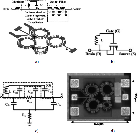
A 60 GHz rectenna was developed with MMIC technology at Eindhoven University of Technology, the Netherlands [GAO 13]. They indicated that several low-impedance paths caused by parasitic capacitances lead to a trade-off between isolation and insertion-loss at 60 GHz. Therefore, the inductor-peaked rectifier structure was proposed and realized (Figure 3.85). An inductor-peaked diode-connected transistor, self-threshold voltage modulation and a low-pass output filter are used to increase the sensitivity and the efficiency of the rectifier. The series input inductor can take advantage of the voltage boost effect. The designed rectifier reaches 7% efficiency at 62 GHz with −14 dBm input.
Figure 3.85. Rectenna of 60 GHz. a) Schematic of inductor-peaked rectifier and layout model for electromagnetic field simulation; b) inductor-peaked diode-connected transistor; c) circuit model in the on-state; d) die micrograph of 62 GHz inductor-peaked rectifier[GUH 13]
Various other RF and microwave harvester modules have been reported in the literature: amplitude modulation (AM broadcasting radio [WAN 13], broadcasting TV [SAM 09, KAW 13], Global System for mobile communications (GSM) [POW 13], global positioning system (GPS) [ZHU 11], X-band [EPP 00] and K-band [TAK 13].
Dual-band rectennas are useful for various applications. A 2.45 and 5.8 GHz dual-band rectenna, in which a singleshunt rectifier was used, was developed at Texas A&M University (Figure 3.86) [SUH 02].
Figure 3.86. a) Dual-band rectenna developed at Texas A&M University and b)RF–DC conversion efficiency and reflection ratio of dual-band rectenna [SUH 02]

A triple-band rectenna (900 MHz, 1.9 GHz and 2.4 GHz) was also developed at the University of California, Davis (Figure 3.87) [PHA 13]. The antenna was designed using a combination of three different design techniques including a composite right/left-hand transmission line. For the rectifier, which was of the charge-pump type, they tuned each matching frequency independently.
Figure 3.87. Triple-band rectenna developed at UC Davis. a) Schematic diagram of proposed rectifier, b) RF–DC conversion efficiency and c) image of triple-band antenna and rectifier [PLA 13]
3.5.4. Various rectennas III – weak power and energy harvester
For energy harvesting, a high-efficiency rectenna capable of harvesting weak power signals is required. It is also important to realize an MPT to sensor network or weak power MPT applications suitable for an initial commercial phase. As mentioned in section 3.2, a rectenna with a diode usually cannot realize high efficiency at weak power. The VJ effect cannot increase the efficiency. So we should consider how we can add a higher voltage to VJ on a diode without any extra power source.
There are some high-efficiency rectennas operating at weak power, and they use various circuits as follows:
The charge-pump rectifier (Figure 3.88) is currently in common use for energy harvesting or weak power MPT because the required diode voltage can be created. But its RF–DC conversion efficiency is generally low because many diodes and many capacitances are needed to increase the voltage.
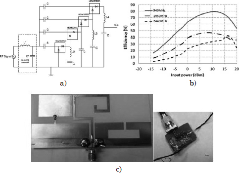
To increase voltage on a diode, some groups have used a resonator. Tohoku University’s group used a short-stub resonator (Figure 3.89(a)) [KIT 06]. They achieved an RF–DC conversion efficiency of ~40% at 900 MHz and 10 µW. Toyama University’s group adopted an L–C resonator and a dielectric resonator (Figures 3.89(b) and (c)) [YAM 13].
Figure 3.88. Charge-pump rectifier. a) Schematic and b) implementation [YAN 13]
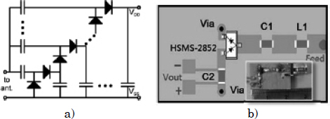
Figure 3.89. Rectifier with a resonator. a) With a short-stub [KIT 06], b) with an L-C resonator [YAM 13] and c) with a dielectric resonator [YAM 13]
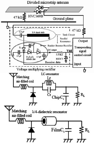
Utilization of the reflected microwave and the standing wave is a feasible means of increasing the voltage on a diode. Okayama University’s group tried to develop a system based on this concept [UED 04]. They used the reflected microwave from an output filter. Kyoto University and Mitsubishi Electric Corp. also focused on the output filter to increase RF–DC conversion efficiency. For the output filter, a distributed line length of λg/4 must be used to realize a full-wave rectifier with a single shunt [GUT 79]. But we also searched for the optimum highest length of the distributed line on the output filter to achieve the highest RF–DC conversion efficiency at 1 mW and 5.8 GHz. We found that <λg/10 distributed line is optimal (Figure 3.90(a)) and we experimentally achieved more than 50% efficiency at 1 mW and 5.8 GHz. For a 2.45 GHz rectenna, we additionally considered the number of diodes as shown in Figure 3.90(b). Finally, we achieved 55.3% efficiency at 0.1 mW and 8.2 kΩ at 2.45 GHz in a circuit simulation.
Figure 3.90. Rectifier with the design of an output filter. a) With <λg/10 distributed line at 5.8 GHz [SHI 04, SHI 13] and b) with optimization of number of diodes and length of distributed lines at 2.45 GHz [SHI 13]

A zero-bias diode is a device which could potentially be used to increase the RF–DC conversion efficiency for weak microwave signals. Some trials have been conducted using a zero-bias diode but the RF–DC conversion efficiency is still low [TAK 13, ZBI 06].
3.5.5. Rectenna array
A rectenna will normally be used as an array for high-power MPT because one rectenna element only rectifies a few W. Although there are many existing studies of rectenna elements as discussed in previous sections, only a few rectenna arrays have been developed and used for experiments (such as the array shown in Figure 3.91). The largest rectenna array in the world was used for a ground-to-ground experiment in Goldstone, USA, by JPL in 1975 as shown in section 1.2. The size was 3.4 m × 7.2 m = 24.5 m2. A rectenna array that had 2,304 elements and was 3.54 m × 3.2 m in size was developed for a ground-to-ground experiment conducted by Kyoto University, Kobe University, and Kansai Electric Corporation in 1994. Kyoto University has several types of rectenna arrays designed for 2.45 and 5.8 GHz operation. The area of these arrays is approximately 1 mϕ. Another rectenna array with a size of 2.7 m × 3.4 m was developed for a fuel-free airship MPT experiment conducted by CRL and Kobe University in Japan in 1995. A large rectenna was developed for a Reunion Island project, as previously shown in Figure 1.9.
For usual phased array antenna applications for radar systems, etc. mutual coupling and phase distribution are the problems which need to be solved. For the rectenna array, the problem is different from that of the array antenna because it is connected in the DC domain that includes no phase. Figure 3.92 shows the beam pattern of an antenna element that is assumed to be a cosine pattern for an array with normal antennas and an array with rectennas, respectively. Maximum power is normalized for each array. The beam pattern becomes narrower when antenna elements are connected in an array. But the beam of the rectenna array does not become narrower and is the same as that of one antenna element. This is due to the DC connection in the rectenna array where phase coupling is not an issue.
Figure 3.91. Large rectenna arrays used for a) G-to-G experiment in Goldstone in 1975, b) G-to-G experiment in Japan in 1994–1995, c) fuel-free airship experiment in 1995, d) experimental equipment in Kyoto University

Figure 3.92. Cosine beam pattern of antenna element, array with normal antennas and array with rectenna

A rectenna has the characteristics of RF–DC conversion efficiency shown in Figure 3.69. It depends on an optimum connected load to achieve maximum RF–DC conversion efficiency at a given microwave frequency. The characteristics of the RF–DC conversion efficiency can be explained by the maximum power transfer theorem based on the equivalent circuit of a rectifying circuit that consists of a DC source and an internal resistance (Figure 3.93). When RL = Rs, power supply is at the maximum and corresponds to the maximum RF–DC conversion efficiency. The internal resistance is not a real resistance. V-I curve of a diode as shown in Figure 3.70 creases the characteristics of the RF–DC conversion efficiency of the rectenna which can be explained with the ‘image’ internal resistance. In many rectennas, Rs is approximately several hundred Ohms, depending on the V-I characteristics of the Si Schottky barrier diode or other diode types. This means that the rectifying circuit in a rectenna is considered as a theoretical circuit with a DC power source feeding an internal resistance of several hundred Ohms. A load of several hundred Ohms is too small for a normal DC power supply, so we always have to consider the optimum load to apply the rectenna.
Figure 3.93. Equivalent circuit of rectifying circuit

When two rectennas are connected in series or in parallel, the optimum load requirement changes. Figure 3.94 shows experimental results of a rectenna array conducted in 1994–1995 by Kyoto University [SHI 98b]. In this experiment, 256 rectenna panels composed of nine rectennas connected in parallel were used, and the connections of the rectenna panels were changed from 128 in series and 2 in parallel to 8 in series and 32 in parallel. Figure 3.94 shows the load dependence of the reconfigured array, where the horizontal axis indicates the normalized resistance. The normalizing resistance RN was predicted by theoretical calculations based on the equivalent circuits shown in Figure 3.95. If two rectennas are connected in series, the optimum resistance of the array becomes Rs1 + Rs2. If two rectennas are connected in parallel, the optimum resistance becomes (1/Rs1 + 1/Rs2)−1. These simple theoretical results are supported by the experimental results shown in Figure 3.94. This means that the optimum load can be predicted on the basis of how rectennas are connected in an array.
When the amplitude of the input microwave power supplied to two connected rectennas is different, for example VS1>>VS2, they will not operate at their optimum points and their combined DC output would be less than if they were operated independently. This can be explained by the characteristics of RF–DC conversion efficiency. It has been experimentally and theoretically proven that the total DC output decreases with a series connection to a greater extent than with a parallel connection [SHI 98b]. It has been further confirmed by simulation and experiments that current equalization in a series connection is worse than voltage equalization in a parallel connection [MIU 01]. Thus, parallel connections are the optimum connections for rectenna arrays receiving microwave signals with significant differences in power levels.
Figure 3.94. Connected load dependence of a rectenna array; a) output DC current, b) output DC voltage and c) output DC power [SHI 98b]
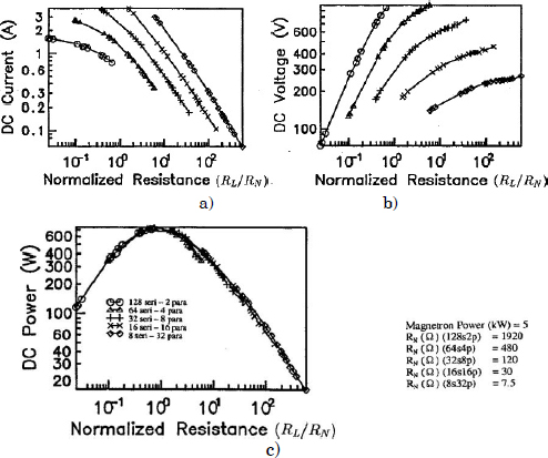
Figure 3.95. Equivalent circuits of rectifying circuit: a) connected in series and b) connected in parallel

3.5.6. Rectifier using vacuum tube
We can not only use a rectenna as a rectifier, but in certain situations we can also use a vacuum tube. If we would like to use a parabolic antenna as an MPT receiver, we use a cyclotron wave converter (CWC) instead of a rectenna. The CWC is a microwave vacuum tube used to rectify high-power microwaves directly into DC power. The most studied CWC consists of an electron gun, a microwave cavity with uniform transverse electric field in the interaction gap, a region with a symmetrically reversed (or decreasing to zero) static magnetic field and a collector with depressed potential, as shown in Figure 3.96. Microwave power from an external source is converted by this coupler into the energy for the electron beam rotation, and the latter is transformed into additional energy for the longitudinal motion of the electron beam by a reversed static magnetic field; then, the energy is extracted by decelerating the electric field of the collector and appears as a DC signal at the load resistance of this collector.
Figure 3.96. Schematic of a cyclotron wave converter

The first CWC experiment was carried out by Watson et al. [WAT 68, WAT 66, WAT 70]. The first CWC could only rectify 1–1.5 W input with 56% efficiency. At Moscow State University, a variant of the CWC was tested and its efficiency was 70–74% at 2.5–25 W. The TORIY Corporation and Moscow State University collaborated to create several high-power CWCs with efficiencies of 60–83% at 10–20 kW [VAN 82, VAN 91, VAN 95]. They demonstrated the CWC at the WPT ’95 conference in Kobe, Japan. Vanke’s group has continued to improve the CWC (Figure 3.62) [VAN 98, VAN 03]. A European group plans to apply a CWC for a ground-to-ground MPT experiment on Reunion Island [CEL 04], but this project has not yet been carried out.
Brown also proposed the use of a vacuum microwave rectifier in the 1960s [BRO 64]. He proposed a rectifier based on multipactor discharge. The term “multipactor” is derived from the words “multiple electron impact”. A multipactor discharge consists of a thin electron cloud that is driven back and forth across a gap in response to an RF field applied across the gap. For the discharge to be self-sustaining, the second emission coefficient of the surface of the electrodes must be greater than unity, and the magnitude and frequency of the applied RF field must be adjusted so that the electron cloud traverses the gap during the half-cycle of the RF field. Under these conditions, successive impacts of the electron cloud produce a greater electron density, and the secondary electrons created with each impact are driven to the opposite electrode, producing additional secondary charge. Thus, the discharge current builds up. As the electron density increases, however, mutual repulsion causes some of the electrons to fall out of step with the field and thus limit the maximum electron density to a value controlled by the secondary emission coefficient [FOR 59].
Figure 3.97. CWCs developed in Russia [VAN 03]
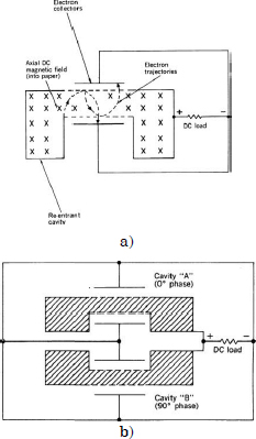
Multipactor discharges can be used to provide both half-wave and full-wave rectification. A full-wave rectifier utilizes a re-entrant microwave cavity with the electric field concentrated at the center of the cavity where the secondary emitting electrodes are located (Figure 3.98) [BRO 64]. A single-cavity full-wave rectifier and a dual-cavity two-phase full-wave rectifier are shown in Figures 3.99(a) and (b), respectively. If the DC load voltage has been set equal to the electron impact voltage, the RF–DC conversion efficiency of the single-cavity full-wave rectifier is theoretically 59%, and that of the dual-cavity two-phase rectifier theoretically approaches 92% or approximately π/2 times that of the single-cavity full-wave rectifier.
Figure 3.98. Full-wave multipactor rectifier cavity [BRO 64]
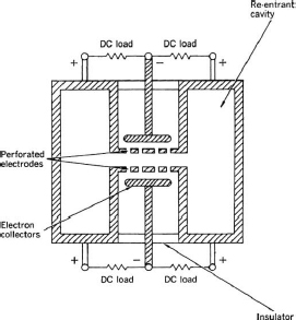
Figure 3.99. a) Single-cavity full-wave rectifier. b) Dual-cavity two-phase rectifier [BRO 64]