
Chapter 4: Developing Your First FPGA Program
This chapter begins with a discussion on the effective use of FPGA devices in real-time embedded systems and continues with a description of the functional elements contained within standard FPGAs. The range of FPGA design languages, including Hardware Description Languages (HDLs), block diagram methods, and popular software programming languages including C and C++, is introduced. The chapter continues with an overview of the FPGA development process and concludes with a complete example of an FPGA development cycle starting with a statement of system requirements and ending with a functional system implemented in a low-cost FPGA development board.
After completing this chapter, you will know how FPGAs can be applied in real-time embedded system architectures and will understand the components that make up an FPGA integrated circuit. You will have learned about the programming languages used in the design of FPGA algorithms and will understand the sequence of steps to develop an FPGA-based application. You will also have worked through a complete FPGA development example on a low-cost development board using free FPGA software tools.
We will cover the following topics in this chapter:
- Using FPGAs in real-time embedded system designs
- FPGA implementation languages
- The FPGA development process
- Developing your first FPGA project
Technical requirements
The files for this chapter are available at https://github.com/PacktPublishing/Architecting-High-Performance-Embedded-Systems.
Using FPGAs in real-time embedded system designs
As we saw in the Elements of FPGAs section of Chapter 1, Architecting High-Performance Embedded Systems, a typical FPGA device contains a large number of lookup tables, flip-flops, block RAM elements, DSP slices, and other components. While it can be instructive to understand the detailed capabilities of each of these components, such concerns are not necessarily informative during the FPGA development process. The most important constraint to keep in mind is that a specific FPGA part number contains a finite number of each of these elements, and a design cannot exceed those limits when targeted at that particular FPGA model.
Instead, it is more productive to view the FPGA development process from the perspective of the embedded system's statement of requirements. You can begin to develop the FPGA design targeted at a somewhat arbitrarily chosen FPGA model. As development proceeds, you may reach a resource limit or identify an FPGA feature the design requires that is not present in the currently targeted FPGA. At that point, you can select a different, more capable, target and continue development.
Alternatively, as development of the design nears completion, you may realize the target FPGA you originally selected contains excessive resources and the design could be improved by selecting a smaller FPGA, with potential benefits in terms of lower cost, fewer pins, smaller package size, and reduced power consumption.
In either of these situations, it is generally straightforward to switch the targeted FPGA to a different model within the same family. The development tools and design artifacts you have created to this point should be fully reusable with the newly targeted FPGA model. If it becomes necessary to switch to a different family of FPGAs from the same vendor, or to a model from a different vendor, the switchover will likely involve more work.
The point of this discussion is to emphasize that it is not too important to identify a specific FPGA model at the outset of a high-performance embedded system development effort. Instead, early considerations should focus on validating the decision to use an FPGA as part of the design, then, if the FPGA is the best design approach, proceed with the selection of a suitable FPGA vendor and device family.
Example projects in this book will be based on the Xilinx Vivado family of FPGA development tools. Although a Vivado license must be purchased to develop for some Xilinx FPGA families, the FPGA devices in the Artix-7 we will be working with are supported by Vivado for free. The Artix-7 FPGA family combines the attributes of high performance, low power consumption, and reduced total system cost. Similar FPGA device families and development tool suites are available from other FPGA vendors.
FPGA development is a fairly involved process, with a variety of types of analysis and design data input required. To avoid discussing these topics at too abstract a level, and to present concrete results in terms of working example projects, we will be using Vivado throughout the book. Once you are familiar with the tools and techniques discussed here, you should be able to apply them using similar tools from other vendors.
The following sections will discuss some key differentiating features of the families of FPGAs and individual models within those families, including the quantity of block RAM, the quantity and types of I/O signals available, specialized on-chip hardware resources, and the inclusion of one or more hardware processor cores in the FPGA package.
Block RAM and distributed RAM
Block RAM is used to implement regions of memory within an FPGA. A particular memory region is specified in terms of the width in bits (typically 8 or 16 bits) and the depth, which defines the number of storage locations in the memory region.
The total quantity of block RAM in an FPGA is usually specified in terms of kilobits (Kb). The amount of block RAM available varies across FPGA families and among the models within a particular family. As you would expect, larger, more expensive parts generally have a greater quantity of resources that can be used as block RAM.
In Xilinx FPGAs, and to varying degrees in FPGAs from other vendors, a distinct category of memory called distributed RAM is available in addition to block RAM. Distributed RAM is constructed from the logic elements used in lookup tables and repurposes the circuitry of those devices to form tiny segments of RAM, each containing 16 bits. These segments can be aggregated to form larger memory blocks when necessary.
Block RAM tends to be used for purposes traditionally associated with RAM, such as implementing processor cache memory or as a storage buffer for I/O data. Distributed RAM might be used for purposes such as the temporary storage of intermediate computation results. Because distributed RAM is based on lookup table circuitry, the use of distributed RAM in a design reduces the resources available for implementing logic operations.
Block RAM can have a single port or dual ports. Single-port block RAM represents the common usage pattern of a processor that reads and writes RAM during operation. Dual-port block RAM provides two read/write ports, both of which can be actively reading or writing the same memory region simultaneously.
Dual-port block RAM is ideal for situations where data is being transferred between portions of an FPGA running at differing clock speeds. For example, an I/O subsystem might have a clock speed in the hundreds of MHz as it receives an incoming data stream. The I/O subsystem writes incoming data to the block RAM as it arrives through one of the FPGA's high-speed I/O channels. A separate subsystem with the FPGA, running at a different clock speed, can read data from the block RAM's second port without interfering with the operation of the I/O subsystem.
Block RAM can also operate in first-in-first-out (FIFO) mode. In the example of the incoming serial data stream, the I/O subsystem can insert data words into the FIFO as they arrive and the processing subsystem can read them out in the same order. Block RAM in FIFO mode provides signals indicating whether the FIFO is full, empty, almost full, or almost empty. The definitions of almost full and almost empty are up to the system designer. If you assign almost empty to mean less than 16 items are left in the FIFO, you can then be assured that any time the FIFO does not indicate it is almost empty, you can read 16 items without further checks of data availability.
When using block RAM in FIFO mode, it is vital that the logic inserting items into the FIFO never attempts to write when the FIFO is full, and the logic reading from the FIFO never attempts to read when the FIFO is empty. If either of these events occurs, the system will either lose data or will attempt to process undefined data.
FPGA I/O pins and associated features
Because FPGAs are intended for use in high-performance applications, their I/O pins are generally capable of implementing a variety of high-speed I/O standards. During the implementation of a design with an FPGA development tool suite, the system developer must perform tasks that include assigning functions to particular pins on the FPGA package and configuring each of those pins to operate with the appropriate interface standard. Additional steps must be performed to associate input and output signals within the FPGA model code with the correct package pins.
At the pin level, individual I/O signals are either single-ended or differential. A single-ended signal is referenced to ground. Traditional Transistor-Transistor Logic (TTL) and Complementary Metal Oxide Semiconductor (CMOS) digital signals operate over a range of 0-5 VDC relative to ground.
Modern FPGAs typically do not support the legacy 5 VDC signal range, but instead support TTL and CMOS signals operating over a reduced voltage range, thereby reducing power consumption and improving speed. Low Voltage TTL (LVTTL) signals operate over a range of 0-3.3VDC. Low Voltage CMOS (LVCMOS) signals are selectable with signaling voltages of 1.2, 1.5, 1.8, 2.5, and 3.3 V. These signal types are named LVCMOS12, LVCMOS15, LVCMOS18, LVCMOS25, and LVCMOS33. Other high-performance single-ended signal types are available, including High-Speed Transceiver Logic (HSTL) and Stub-Series Terminated Logic (SSTL).
Single-ended signals are widely used for low-frequency purposes, such as reading pushbutton inputs and lighting LEDs. Single-ended signals are also used in many lower-speed communication protocols such as I2C and SPI. An important drawback of single-ended signals is that any noise coupled into the wires and printed circuit board traces carrying the signal has the potential to corrupt the input to the receiver. This problem can be substantially reduced through the use of differential signaling.
For the highest data transfer rates, differential signaling is the preferred approach. Differential signals use a pair of I/O pins and drive opposing signals onto the two pins. In other words, one pin is driven to a higher voltage and the other pin to a lower voltage to represent a 0 data bit and the pin voltages are reversed to represent a 1 bit. The differential receiver subtracts the two signals to determine whether the data bit is 0 or 1. Because the two wires or traces carrying the differential signal are physically located very close together, any noise that couples into one of the signals will couple to the other one in a very similar manner. The subtraction operation removes the vast majority of the noise, enabling reliable operation at much higher data transfer rates than single-ended signals.
A number of differential signal standards are supported by standard FPGAs. Several differential versions of HSTL and SSTL are defined, with a variety of signaling voltage levels for each.
Low-Voltage Differential Signaling (LVDS) was introduced as a standard in 1994 and continues to be used in a variety of applications. An LVDS signaling transmitter produces a constant current of 3.5 mA and switches the direction of the current flowing through the resistor at the receiver to produce state changes representing 0 and 1 data values as shown in Figure 4.1:
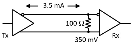
Figure 4.1 – LVDS interface
In LVDS communication, as in the other differential and single-ended signaling standards, it is important for the impedance of the communication path between the transmitter and receiver to closely match the termination impedance, which is 100 Instance 8 in the case of LVDS. If the impedance of the communication channel does not match the termination impedance, reflections can occur on the line, preventing reliable data reception.
The impedance of differential signal trace pairs is a function of the geometry of the pair traces and their relationship to the ground plane. As we will see in Chapter 6, Designing Circuits with KiCad, it is straightforward to design circuit boards that satisfy the requirements of high-speed differential signaling standards.
Specialized hardware resources
FPGAs generally include a selection of dedicated hardware resources for functions that are commonly required and are either more efficiently implemented in hardware rather than using synthesized FPGA functions, or not possible to implement with FPGA components. Some examples of these resources are as follows:
- Interfaces to external dynamic RAM (DRAM) for storing large quantities of data. These interfaces generally support a common DRAM standard such as DDR3.
- Analog-to-digital converters.
- Phase-locked loops, used for generating multiple clock frequencies.
- Digital signal processing multiply-accumulate (MAC) hardware.
These hardware resources enable the development of complex systems with wide-ranging capabilities. Dedicated hardware is provided for functions like the MAC operation because the hardware performance is significantly better than the synthesized equivalent functionality using FPGA logic resources.
Processor cores
Some FPGA families include hardware processor cores for the purpose of combining peak software execution speed with the performance advantages of FPGA-implemented algorithms. For example, the Xilinx Zynq-7000 family integrates a hardware ARM Cortex-A9 processor together with a traditional FPGA fabric.
FPGA designs that do not require a hardware processor can implement a processor using the FPGA resources, referred to as a soft processor. Soft processors are highly configurable, though they are generally not capable of matching the performance of a processor implemented in hardware.
The next section will introduce the primary programming languages and data entry methods used to develop FPGA algorithms.
FPGA implementation languages
Implementing a design for an FPGA ultimately comes down to using one or more software-programming-like languages to define the functionality of the device. The traditional languages used for FPGA development are VHDL and Verilog. Current-generation FPGA development tools generally support both of these languages together with the ability to define system configurations using block diagramming techniques. Some tool suites also support the definition of FPGA functionality using the traditional C and C++ programming languages.
VHDL
VHSIC Hardware Description Language (VHDL), where VHSIC stands for Very High-Speed Integrated Circuit, has syntax reminiscent of the Ada programming language. VHDL was developed under the guidance of the US Department of Defense beginning in 1983.
Like Ada, VHDL tends to be quite verbose and rigidly structured. In programming language terms, VHDL is strongly typed. The language contains a predefined set of base data types, principally boolean, bit, bit_vector, character, string, integer, real, time, and array. All other data types are defined in terms of the base types.
A set of VHDL libraries has been defined by the Institute of Electrical and Electronics Engineers (IEEE) and formalized as the IEEE 1164 standard, Multivalue Logic System for VHDL Model Interoperability. These libraries define the set of logic values to be used in the VHDL language. This library includes a type named std_logic, which represents, a 1-bit signal. The logical values within the std_logic type are represented by the character literals shown in the following table:

The "strong" 0 and 1 values in the preceding figure represent signals driven to the specified binary state. The "weak" signals represent signals driven on a bus with multiple drivers where any driver can assert itself on the bus, overriding the other drivers. The Z value represents a CMOS output in the high-impedance state, where rather than driving the bus to a 0 or 1 state, the output is instead effectively disconnected from the bus and does not drive it at all. The U state represents the default values for all signals. When performing circuit simulation, any signal in the U state will be detected, which likely indicates an uninitialized value is being used unintentionally. The X state is associated with wires that do not have any outputs driving them. The – state represents inputs that are unused, and therefore it does not matter what state they are in.
VHDL circuit designs generally begin by importing the IEEE 1164 libraries via the following statements:
library IEEE;
use IEEE.std_logic_1164.all;
We will use VHDL in our project example later in the chapter. This is not intended to represent a strong preference for VHDL over Verilog. Both hardware definition languages are fully capable of representing essentially any design that can be synthesized for an FPGA.
Verilog
The Verilog Hardware Description Language (HDL) was introduced in 1984 and became standardized as IEEE 1364 in 2005. In 2009, the Verilog standard was combined with the SystemVerilog standard to produce IEEE Standard 1800-2009. SystemVerilog contains extensive facilities for performing system verification, in addition to the hardware design features present in Verilog.
Verilog was designed to resemble the C programming language, including similar operator precedence and the use of some of the same control flow keywords, including if, else, for, and while.
Verilog uses the concept of a wire to represent signal states. A signal value can take any of the values 0, 1, don't care (x), or high impedance (z), and can have a strong or weak signal strength.
Both VHDL and Verilog define language subsets that can be used to design logic circuitry. These subsets are referred to as the synthesizable language subsets. Additional language features beyond the synthesizable subsets are available to support tasks such as circuit simulation. We'll see an example of this later in this chapter.
Non-synthesizable language constructs tend to behave more like traditional software programming languages. For example, a non-synthesizable for loop iterates through a block of code sequentially the specified number of times, just like in a regular programming language. A synthesizable for loop, on the other hand, becomes effectively unrolled to generate a collection of replicated hardware constructs that execute in parallel representing each iteration of the loop.
Block diagrams
At a level of abstraction above the text-based HDLs, modern FPGA development tool suites support the rapid configuration of system designs incorporating complex logic components such as microprocessors and sophisticated I/O devices using a block structure format. Figure 4.2 is an example of a portion of a block diagram for a Xilinx FPGA design incorporating a MicroBlaze soft processor:
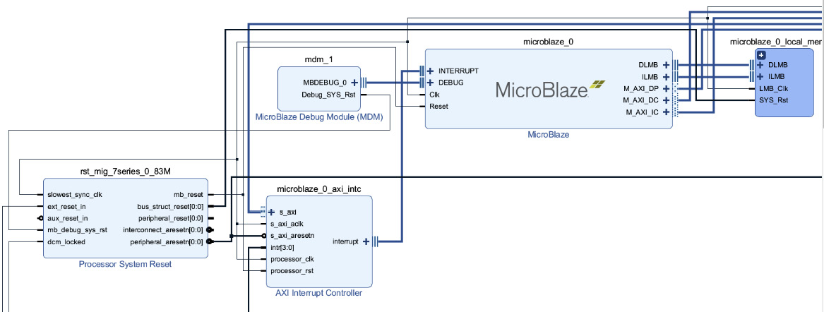
Figure 4.2 – Block diagram containing a MicroBlaze soft microprocessor
The MicroBlaze processor is a processor core provided with the Xilinx Vivado tool suite for use in FPGA designs in processor families including the Artix-7.
While the use of block diagrams provides a visually intuitive way to organize the instantiation and interconnection of complex logic elements in an FPGA design, it is important to remember that behind the diagram, the development tool generates VHDL or Verilog code to define the components and their connections. The block diagram is simply a user interface for managing the configuration of these components.
After you develop a block diagram, you can examine the generated HDL code, which will be contained in files associated with the project. In the diagram of Figure 4.2, a file named design_1_microblaze_0_0_stub.vhdl is produced from the diagram. This file begins with the following VHDL code:
library IEEE;
use IEEE.STD_LOGIC_1164.ALL;
entity design_1_microblaze_0_0 is
Port (
Clk : in STD_LOGIC;
Reset : in STD_LOGIC;
Interrupt : in STD_LOGIC;
Interrupt_Address : in STD_LOGIC_VECTOR ( 0 to 31 );
Interrupt_Ack : out STD_LOGIC_VECTOR ( 0 to 1 );
Instr_Addr : out STD_LOGIC_VECTOR ( 0 to 31 );
Instr : in STD_LOGIC_VECTOR ( 0 to 31 );
This code begins with a reference to the IEEE 1164 standard library, then defines an interface to the MicroBlaze processor that exposes the signals you would expect on a microprocessor, including the system clock, reset, interrupt request, and interrupt vector inputs; interrupt acknowledge and instruction address outputs; and a bus for the instructions retrieved from memory.
This code makes use of the IEEE 1164 library data types for single-bit signals (STD_LOGIC) and for multi-bit bus signals (STD_LOGIC_VECTOR).
The code in the listing defines the interface to the MicroBlaze processor, but it does not contain the HDL definition of the processor itself. Complex HDL designs for components such as microprocessors are considered valuable Intellectual Property (IP) and the commercial entities that develop these designs often take steps to ensure they are not used without appropriate licensing. When vendors distribute IP for use by their customers, it may be provided in a compiled format that is opaque to end users. This allows users to incorporate the IP into their designs, but they cannot examine the HDL used to develop it. This is conceptually similar to software developers who release a library in compiled form but do not provide the source code.
C/C++
A number of vendors offer software tools that translate traditional high-level programming languages, often C and C++, into HDL code for use in FPGA development. This approach may be attractive if you have a complex algorithm in C or C++ that you would like to accelerate in an FPGA implementation. These tools also allow software developers who are familiar with C/C++ to immediately begin implementing code for FPGA use without a need to learn one of the HDLs.
While FPGA development tools for these high-level languages are capable of significant optimization of the resulting FPGA implementation of the C/C++ code algorithm, there is still something of a disconnect in that the C/C++ execution model involves the sequential execution of statements while the native FPGA environment consists of parallel hardware components. The FPGA design resulting from C/C++ code typically resembles a collection of state machines that manage the sequential execution of the operations defined in the programming language statements. Depending on the availability of opportunities for parallel execution within the C/C++ code, an FPGA implementation may provide a significant performance enhancement compared to running the same code on a traditional processor.
In modern FPGA development tool suites, all of the methods of FPGA implementation described in this section (VHDL, Verilog, block diagrams, and C/C++) can be combined in a single design, if needed. Because of this, one team member may prefer to work in VHDL while another uses Verilog. There may be project management reasons for discouraging multi-HDL use within a single project, but the languages themselves function together in a single design without issue. One reason a project manager may wish to avoid the use of multiple HDLs is that the future sustainment of the effort will require the participation of developers with skills in both languages.
Similarly, it is possible to define a high-level architecture for a project in terms of a block diagram and then implement detailed subsystem functionality using the HDL of choice. In the same design, it is also possible to integrate HDL generated from a C/C++ algorithm. Embedded system architects and developers should carefully consider the implications and select the appropriate implementation method for each portion of an FPGA design.
The next section will introduce the steps in the standard FPGA development process.
The FPGA development process
While FPGAs are used across a wide variety of disparate application domains, it is possible to identify a set of development steps that are broadly applicable to any FPGA development project. This section discusses the usual FPGA development steps in the sequence they normally occur during a project.
Defining system requirements
The first step in developing a new system, or when initiating a significant upgrade to an existing system, is to develop a clear and detailed understanding of what the system is supposed to do. The requirements definition process begins with a general description of the system's intended functionality, operating modes, and key features. This information should be written out in clear and unambiguous language and shared with all parties having a stake in the success of the development effort. The goal of sharing the system requirements is to achieve consensus among all of the parties as to the completeness and correctness of the descriptions.
Requirement descriptions must be fleshed out to include specifications for the required level of system performance in terms such as sampling rates of input signals and update rates for actuator output commands. Additional details such as physical size constraints, minimum battery lifetime, and tolerable environmental temperature ranges will guide the design process. In general, a comprehensive set of specifications must be developed that describes the minimum performance thresholds for all system parameters that are judged to be relevant to overall system success.
The full set of system requirements must be complete to the extent that any design solution that complies with all of the stated specifications must be an adequate solution. If it turns out that a design that satisfies all of the specifications is deemed unacceptable for some unrelated reason, this represents a failure to fully state the system requirements. For example, if a technically adequate solution is determined to be too expensive to produce, the source of the problem is likely to be a failure to fully define cost containment constraints during the requirements development process.
After the top-level system requirements have been defined and agreed upon, it is generally necessary to divide the overall system configuration into a collection of subsystems, each with a cohesive purpose and its own set of descriptive requirements and technical specifications. In a real-time embedded system architecture, the digital processing capability is likely to be represented as a subsystem with a corresponding collection of requirements
Allocating functionality to the FPGA
If the requirements for digital processing in a system architecture exceed the capabilities of microcontrollers and microprocessors that would otherwise be suitable for use in the system, it may be appropriate to consider incorporating an FPGA in the design. Some system architectures, particularly those that benefit from high-speed digital hardware performing parallel operations, are natural candidates for FPGA implementation. Other system architectures may be capable of adequate performance with traditional digital processing, but there may be valuable opportunities to take advantage of the flexibility and extensibility offered by an FPGA implementation over a planned lifetime that envisions substantial system upgrades in the future.
After the decision has been made to incorporate an FPGA in the design, the next step is to allocate the portions of overall system digital processing requirements to the FPGA device. This typically includes the specification of the FPGA input and output signals, the update rates of inputs and outputs, and the identification of components with which the FPGA must interact, including parts such as ADCs and RAM devices.
Identifying required FPGA features
Having defined the functions to be performed by the FPGA, and with knowledge of the interfaces to other devices that the FPGA must support, it becomes possible to develop a list of features that candidate FPGA devices must provide.
Some FPGA families are designed for low-cost, less-complex applications and thus offer a limited set of resources for implementing digital logic. These devices might operate from battery power and require only passive cooling. Other, more powerful, FPGA families support large-scale, full-featured digital designs, are intended to operate at peak performance, and may require continuous active cooling.
The system requirements associated with the embedded application will guide the selection of an appropriate FPGA family for the application. At this point, it is likely not possible to identify a specific FPGA model within the preferred family because the resource requirements of the FPGA implementation have not been fully defined. However, with experience, it is possible to identify a small number of FPGA models that appear suitable for the design.
In addition to the FPGA resources for digital circuit implementation, many FPGA models include additional features that may be important for the system design. For example, a built-in ADC may be useful for minimizing the system parts count. The list of required and desired FPGA features will help further narrow the selection of appropriate FPGA devices for the system.
Implementing the FPGA design
Having identified a candidate FPGA model, and with the detailed definition of the functionality allocated to the FPGA in hand, it is time to begin the implementation of the FPGA design. This will generally involve the use of the FPGA development tool suite and usually consists largely of developing HDL code in the preferred language for the project.
If appropriate, the FPGA implementation might begin with a block diagram representation of the top-level FPGA design. As necessary, components developed in HDL or C/C++ can be incorporated into the block design to complete the full system implementation.
Alternatively, it is also common for entire system designs to be developed directly in HDL. For developers familiar with the language and with a full understanding of the features and constraints of the FPGA model in use, this may lead to the most resource-efficient and highest-performing design outcome.
FPGA development proceeds in phases as the initial design becomes specified in more detail until a programming file for the FPGA device is produced. It is common to iterate through these phases several times for a large project, developing a small portion of the total design during each pass through the steps. These phases are described in the following sections.
Design entry
Design entry is the phase where the system developer defines system functionality using HDL code, block diagrams, and/or C/C++ code. The code and other artifacts, such as block diagrams, define the logical functionality of the system in abstract terms. In other words, the design artifacts define a logic circuit, but they don't define how it is integrated with the rest of the system.
I/O planning
FPGA I/O planning is the process of identifying the pins assigned to perform particular I/O functions and associating any device features such as the I/O signal standard to use for each signal. As part of the I/O planning process, it may be important to consider issues such as where on the physical device package I/O pins are located. This step is important to minimize the printed circuit board trace lengths for high-speed signals and to avoid forcing circuit signal traces to unnecessarily cross over one another.
The definition of I/O signal requirements is one form of constraint in the FPGA development process. The other primary constraint category consists of timing requirements that determine the FPGA solution's performance. The FPGA synthesis process uses the HDL code and the project constraints to develop a functionally correct FPGA solution that satisfies all of the defined constraints. If the tool cannot satisfy all of the constraints, synthesis will fail.
Synthesis
Synthesis transforms the source code into a circuit design called a netlist. The netlist represents the circuit constructed from the resources of the target FPGA model. The netlist represents a logical, or schematic, version of the circuit. It does not define how the circuit will be implemented in the physical FPGA device. This occurs in the next step.
Place and route
The place process takes the FPGA resources defined in the netlist and assigns them to specific logic elements within the selected FPGA. The resulting resource placements must satisfy any constraints that restrict the allocation of these elements, including I/O constraints and timing constraints.
After the logic elements have been assigned physical locations during the place process, a set of connections among the logic elements is configured during the route process. Routing implements all of the connections between the logic elements and enables the circuit to function as described in the HDL code. After the place and route operations have completed, the configuration of the FPGA is fully determined.
Bitstream generation
The final step in the FPGA development process is the production of a bitstream file. To achieve the highest performance, most modern FPGA devices store their configuration internally using static RAM (SRAM).
You can think of the FPGA configuration SRAM as a very large shift register, containing perhaps millions of bits. The contents of this shift register fully specify all aspects of FPGA device configuration and operation. The bitstream file produced during FPGA development represents the settings for the shift register that cause the device to perform the intended functions specified by the HDL and the constraints. In terms of traditional software development processes, the bitstream file is analogous to an executable program produced by a linker.
SRAM is volatile and loses its contents each time device power is removed. The real-time embedded system architecture must provide a means for loading the bitstream file into the FPGA each time power is applied. Typically, the bitstream is either loaded from flash memory located within the device or from an external source, such as a PC, connected to the device during each power-on cycle.
Having completed the compilation of the FPGA bitstream, the next step is to test the implementation to verify that it operates correctly. This step is no different than the testing required at the end of a traditional software build process.
Testing the implementation
FPGA development is susceptible to all of the types of bugs that bedevil traditional software development efforts. During FPGA development, you will likely be presented with many error messages related to incorrect syntax, attempts to use resources not currently accessible, and many other types of violations. As in any programming endeavor, you will need to identify the source of each error and fix the problem.
Even after the FPGA application successfully proceeds through all of the stages to bitstream generation, there is no guarantee that the design will perform as intended. To achieve a successful design on a reasonable timetable, it is absolutely critical to perform adequate testing at each stage of development.
The first phase of testing should thoroughly exercise the behavior of the HDL code to demonstrate that it performs as intended. The example project at the end of this chapter will demonstrate the use of the Vivado tool suite to perform a thorough test of the HDL logic in the design.
After the bitstream has been generated, there is no substitute for comprehensive testing of the FPGA as implemented in the final system configuration. This testing must thoroughly exercise all features and modes of the FPGA, including its response to out-of-range and error conditions.
At each step of the design, development, and testing process, project personnel must remain attuned to the possibility of implementing system features that are susceptible to improper behavior in unlikely or rare situations. The occurrence of these kinds of issues can represent bugs that are extremely difficult to duplicate and that can forever tarnish the perception of the embedded system design and the organization that produced it. If you do an excellent job of testing, the likelihood of this outcome will be reduced substantially.
The next section provides a detailed description of the steps in the development, testing, and implementation of a simple FPGA project using the Arty A7 development board and the Xilinx Vivado tool suite.
Developing your first FPGA project
In this section, we will develop and implement a simple but complete project using a Xilinx Artix-7 FPGA device installed on a Digilent Arty A7 development board. This board comes in two variants, a lower-cost version (US $129) with a model number ending in-35T and a more capable, but more costly, version (US $249) with a model number ending in -100T. The only difference between the two boards is the model of the Artix-7 FPGA installed on the board. As you would expect, the -35T has fewer resources available than the -100T.
You can use either the -35T or the -100T variant for this project. The only difference in the development process is specifying the correct board model whenever the need arises. However, in later chapters, the -100T variant will be required due to the resource requirements of the example digital oscilloscope project design, so the more capable board is recommended.
The Arty A7 boards are available for purchase at https://store.digilentinc.com/arty-a7-artix-7-fpga-development-board-for-makers-and-hobbyists/ and from other sources, such as Amazon.
For the purpose of this project, the resources on the board of interest are the FPGA device itself, as well as the four switches, four pushbuttons, and five LEDs. This project will demonstrate how to install the Vivado tool suite, create a project, enter HDL code, test the code, and ultimately produce a bitstream and download it to the board. After downloading the bitstream to the board, you will be able to manually test the operation of the system. You will also see how to program the FPGA image into flash memory on the Arty A7 board so that it loads and runs each time the board powers on.
Project description
This project will implement a four-bit binary adder in the FPGA. This is intentionally a very simple design because the focus here is on setting up the tools and learning how to use them, and not on implementing a complex HDL model.
The four switches on the board represent one 4-bit binary number and the four pushbuttons represent another 4-bit number. The FPGA logic will continuously perform an addition operation between these two numbers and display the result as a 4-bit binary number on four LEDs with a fifth LED representing the carry bit.
The 4-bit adder code is based on the single-bit full adder circuit described in the Hardware design languages section of Chapter 1, Architecting High-Performance Embedded Systems.
Installing the Vivado tools
We will use the Xilinx Vivado suite of FPGA development tools for this project and for projects in future chapters. These tools are available for free and are supported on Windows and Linux operating systems. You may install the tools on either operating system. The description in this section covers the Windows version of the tools, but if you are installing on Linux, the differences should be obvious. Working with the Vivado tools should be nearly identical on the different operating systems:
- If you don't already have one, create a Xilinx user account at https://www.xilinx.com/registration/create-account.html.
- Visit https://xilinx.com and log in to your user account. Once logged in, go to the tools download page at https://www.xilinx.com/support/download.html.
- Download the Xilinx Unified Installer: Windows Self-Extracting Web Installer. You should probably select the latest version available, but if you want to follow along with the version used in this book, select version 2020.1.
- The installer file will have a name similar to Xilinx_Unified_2020.1_0602_1208_Win64.exe. Locate this file in your downloads directory and run it. If a dialog warns you about installing an app that isn't Microsoft-verified, click Install anyway.
- When the Welcome screen comes up, click Next:
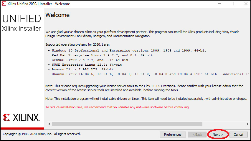
Figure 4.3 – Installer Welcome dialog
- On the following screen, enter your xilinx.com user ID and password, then click Next:

Figure 4.4 – Installer login dialog
- The next dialog requests that you accept some license agreements. Check the boxes that say I Agree, then click Next.
- In the next dialog, leave Vitis selected as the product to be installed and click Next. Vitis includes the Vivado tool suite along with a collection of other Xilinx development tools:
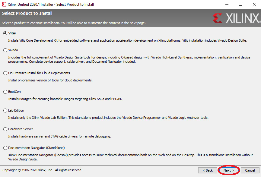
Figure 4.5 – Installer product selection dialog
- The next dialog allows you to select the software components to be installed. Leave the selections at their default values and click Next.
- The next dialog allows you to select a destination directory and specify program shortcut options. A destination directory of C:Xilinx is a suitable location. Create this directory if it does not exist. Click Next.
- The next dialog displays a summary of the installation options. Click Install to proceed with the installation. Depending on the speed of your computer and your internet connection, installation may take a few hours to complete:

Figure 4.6 – Installation complete dialog
Having completed the installation, we will next create our first project.
Creating a project
Follow these steps to create and build the 4-bit binary adder project for the Arty A7 board:
- Locate the desktop icon titled Vivado 2020.1 (or look for your version number, if different) and double-click it.
- When Vivado displays its main screen, click Create Project in the Quick Start section:
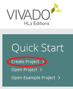
Figure 4.7 – Vivado Quick Start dialog
- This will start the Create a New Vivado Project wizard. Click Next to reach the Project Name page and enter ArtyAdder as the project name. Select an appropriate directory location for the project and check the box to create a subdirectory, then click Next. Examples in this book will use the C:Projects directory as the location for all projects:
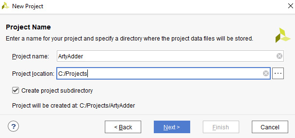
Figure 4.8 – Project Name dialog
- In the Project Type dialog, select RTL Project and check the box next to Do not specify sources at this time. Click Next:
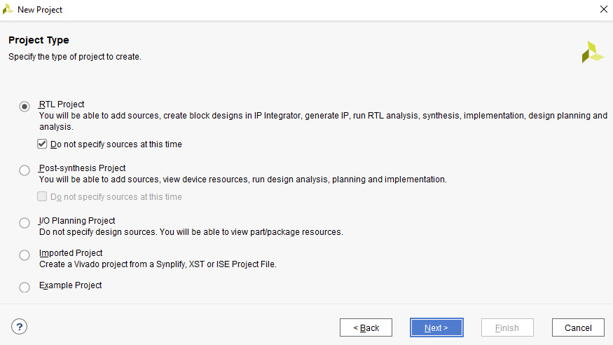
Figure 4.9 – Project Type dialog
- In the Default Part dialog, click the Boards tab and type Arty into the Search field. Depending on the board type you have (or if you don't have a board yet), select either the Arty A7-100 or Arty A7-35 and click Next:
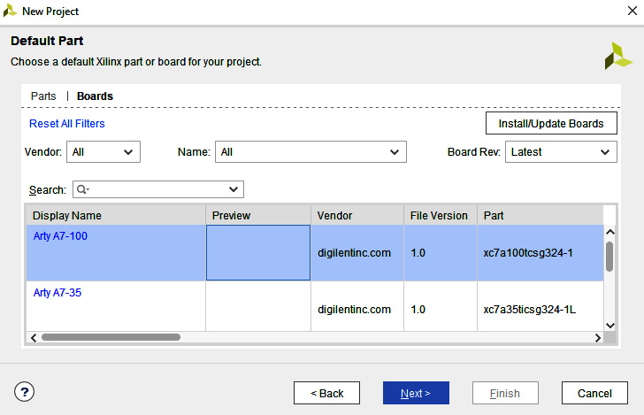
Figure 4.10 – Default Part dialog
- In the New Project Summary dialog, click Finish.
We have now created an empty project. In the next section, we will create VHDL source files containing the logic circuit design for this project.
Creating VHDL source files
The following steps describe the process of creating VHDL source files, entering source code, and compiling the FPGA design:
- In the Sources sub-window, right-click Design Sources and select Add Sources…:

Figure 4.11 – Add Sources… menu selection
- In the Add Sources dialog, ensure Add or create design sources is selected, then click Next.
- In the Add or Create Design Sources dialog, click Create File:
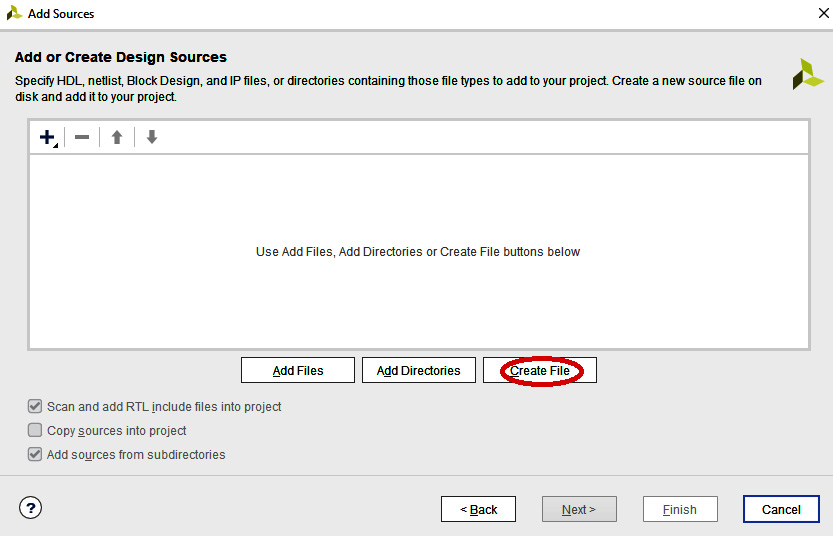
Figure 4.12 – Add or Create Design Sources dialog
- Enter the filename FullAdder.vhdl and click OK:
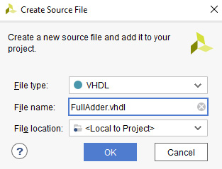
Figure 4.13 – Create Source File dialog
- Repeat the previous two steps to create another file named Adder4.vhdl, then click Finish in the Add or Create Design Sources dialog.
- The Define Modules dialog will appear next. We will not be entering anything here. Click OK to close this dialog. You will be asked if you are sure you want to use these values. Click Yes:
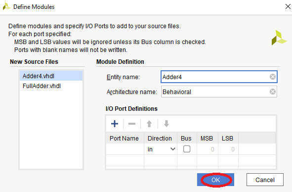
Figure 4.14 – Define Modules dialog
- Expand the Non-module Files under Design Sources, then double-click FullAdder.vhdl. An editor window will open displaying the empty FullAdder.vhdl file:
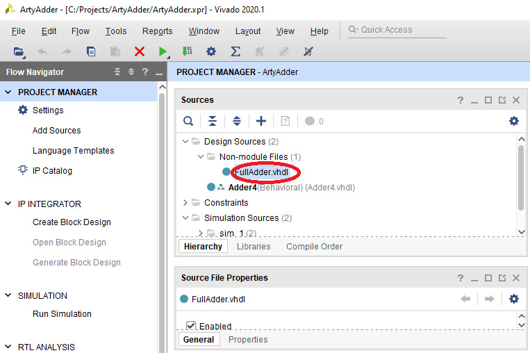
Figure 4.15 – Newly created source file
- Enter the following VHDL code into the FullAdder.vhdl editor window:
-- Load the standard libraries
library IEEE;
use IEEE.STD_LOGIC_1164.ALL;
-- Define the full adder inputs and outputs
entity FULL_ADDER is
port (
A : in std_logic;
B : in std_logic;
C_IN : in std_logic;
S : out std_logic;
C_OUT : out std_logic
);
end entity FULL_ADDER;
-- Define the behavior of the full adder
architecture BEHAVIORAL of FULL_ADDER is
begin
S <= (A XOR B) XOR C_IN;
C_OUT <= (A AND B) OR ((A XOR B) AND C_IN);
end architecture BEHAVIORAL;
This is the same single-bit full adder code we examined in the Hardware design languages section of Chapter 1, Architecting High-Performance Embedded Systems. Figure 4.16 shows the code in the Vivado editor window:
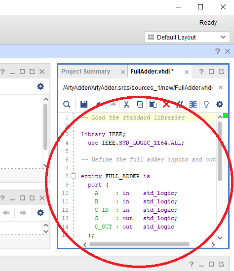
Figure 4.16 – FullAdder.vhdl source code
- In the same manner, double-click Adder4(Behavioral) (Adder4.vhdl) under Design Sources. Delete the automatically populated contents of the Adder4.vhdl editor window and enter the following code into the Adder4.vhdl editor:
-- Load the standard libraries
library IEEE;
use IEEE.STD_LOGIC_1164.ALL;
-- Define the 4-bit adder inputs and outputs
entity ADDER4 is
port (
A4 : in std_logic_vector(3 downto 0);
B4 : in std_logic_vector(3 downto 0);
SUM4 : out std_logic_vector(3 downto 0);
C_OUT4 : out std_logic
);
end entity ADDER4;
-- Define the behavior of the 4-bit adder
architecture BEHAVIORAL of ADDER4 is
-- Reference the previous definition of the full adder
component FULL_ADDER is
port (
A : in std_logic;
B : in std_logic;
C_IN : in std_logic;
S : out std_logic;
C_OUT : out std_logic
);
end component;
-- Define the signals used internally in the 4-bit adder
signal c0, c1, c2 : std_logic;
begin
-- The carry input to the first adder is set to 0
FULL_ADDER0 : FULL_ADDER
port map (
A => A4(0),
B => B4(0),
C_IN => '0',
S => SUM4(0),
C_OUT => c0
);
FULL_ADDER1 : FULL_ADDER
port map (
A => A4(1),
B => B4(1),
C_IN => c0,
S => SUM4(1),
C_OUT => c1
);
FULL_ADDER2 : FULL_ADDER
port map (
A => A4(2),
B => B4(2),
C_IN => c1,
S => SUM4(2),
C_OUT => c2
);
FULL_ADDER3 : FULL_ADDER
port map (
A => A4(3),
B => B4(3),
C_IN => c2,
S => SUM4(3),
C_OUT => C_OUT4
);
end architecture BEHAVIORAL;
This code instantiates four copies of the single-bit full adder. The carry into the least significant adder is set to zero and the carry from each adder ripples to the next most-significant adder. The result of adding two 4-bit numbers is a 4-bit result and a single-bit carry:

Figure 4.17 – Adder4.vhdl source code
At this point, you have entered VHDL code that defines a 4-bit binary adder constructed from four single-bit full adders. Next, we will test the correctness of the implementation.
Testing the logic behavior
It is important to test the behavior of logic using simulation before trying to run it in the FPGA. This is because it is much easier to detect and fix problems in the simulation environment than it is with the logic running inside the FPGA. The Vivado simulation tools do a very good job of representing circuit behavior:
- In the Sources sub-window, right-click on Simulation Sources and select Add Sources…:
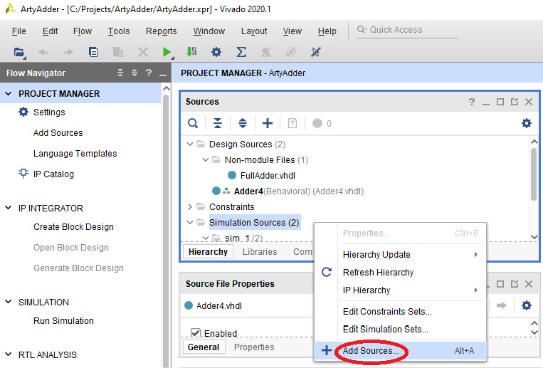
Figure 4.18 – Add Sources… menu selection for Simulation Sources
- In the Add Sources dialog, ensure Add or create simulation sources is selected, then click Next.
- In the Add or Create Simulation Sources dialog, click Create File.
- Enter the filename Adder4TestBench.vhdl and click OK.
- Click Finish to dismiss the Add or Create Simulation Sources dialog, then click OK in the Define Module dialog and click Yes when asked if you are sure you want to use these values.
- Double-click Adder4 TestBench (Behavioral) (Adder4TestBench.vhdl) under Simulation Sources. Delete the automatically populated contents of the Adder4TestBench.vhdl editor window and enter the following code into the Adder4TestBench.vhdl editor:
library IEEE;
use IEEE.STD_LOGIC_1164.ALL;
use IEEE.NUMERIC_STD.ALL;
entity ADDER4_TESTBENCH is
end entity ADDER4_TESTBENCH;
architecture BEHAVIORAL of ADDER4_TESTBENCH is
component ADDER4 is
port (
A4 : in std_logic_vector(3 downto 0);
B4 : in std_logic_vector(3 downto 0);
SUM4 : out std_logic_vector(3 downto 0);
C_OUT4 : out std_logic
);
end component;
signal a : std_logic_vector(3 downto 0);
signal b : std_logic_vector(3 downto 0);
signal s : std_logic_vector(3 downto 0);
signal c_out : std_logic;
signal expected_sum5 : unsigned(4 downto 0);
signal expected_sum4 : unsigned(3 downto 0);
signal expected_c : std_logic;
signal error : std_logic;
begin
TESTED_DEVICE : ADDER4
port map (
A4 => a,
B4 => b,
SUM4 => s,
C_OUT4 => c_out
);
TEST : process
begin
-- Test all combinations of two 4-bit addends (256 total tests)
for a_val in 0 to 15 loop
for b_val in 0 to 15 loop
-- Set the inputs to the ADDER4 component
a <= std_logic_vector(to_unsigned(a_val, a'length));
b <= std_logic_vector(to_unsigned(b_val, b'length));
wait for 1 ns;
-- Compute the 5-bit sum of the two 4-bit values
expected_sum5 <= unsigned('0' & a) + unsigned('0' & b);
wait for 1 ns;
-- Break the sum into a 4-bit output and a carry bit
expected_sum4 <= expected_sum5(3 downto 0);
expected_c <= expected_sum5(4);
wait for 1 ns;
-- The 'error' signal will only go to 1 if an error occurs
if ((unsigned(s) = unsigned(expected_sum4)) and
(c_out = expected_c)) then
error <= '0';
else
error <= '1';
end if;
-- Each pass through the inner loop takes 10 ns
wait for 7 ns;
end loop;
end loop;
wait;
end process TEST;
end architecture BEHAVIORAL;
This code exercises the 4-bit adder functionality by presenting all combinations of 4-bit numbers to each of the A4 and B4 inputs to the Adder4 component. It compares the SUM4 and C_OUT4 outputs of the Adder4 component to independently computed values for the same inputs. After each addition operation, the error signal is set to 0 if the Adder4 outputs matched the expected values, or it is set to 1 if there is a mismatch.
The code in Adder4TestBench.vhdl resembles traditional software code in the way it uses nested for loops to apply all of the test input combinations to the Adder4 component under test. Code that runs tests in simulation mode is non-synthesizable, which means it does not purely represent a hardware logic circuit and is capable of traditional software-like operations, such as the iterative execution of for loops.
However, as in physical circuits, signals being assigned values in the test bench code using the <= operator cannot be used at the same instant in time in subsequent expressions. This is because the simulation environment represents the real-world effects of propagation delay, which is significant even within tiny FPGA devices. The three wait for 1 ns; statements in the test bench code pause circuit operations to allow for propagation delay. These 1 ns delays provide time for the signal values computed just before the wait statement to propagate so they can be used in the following statement. The final wait for 7 ns; statement in the inner loop is a pause that allows us to clearly see the results of each iteration of the simulation loops in the signal trace display.
- Right-click Adder4 TestBench (Behavioral) (Adder4TestBench.vhdl) under Simulation Sources and select Automatic Update and Compile Order. This sets ADDER4_TESTBENCH as the top-level object for the simulation run:
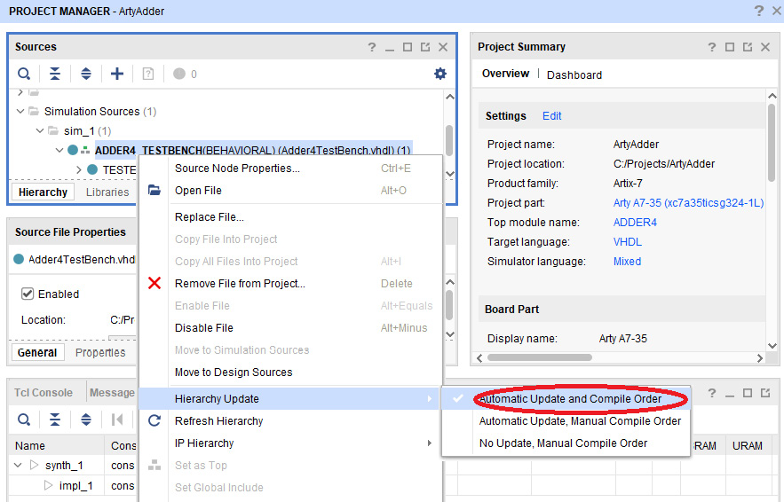
Figure 4.19 – Menu selection to set Automatic Update and Compile Order
- Click Run Simulation, then Run Behavioral Simulation in the Flow Navigator window to enter simulation mode. If you haven't already saved the editor files, you will be prompted to do so. Click Save. The simulation will then run:

Figure 4.20 – Run Behavioral Simulation menu selection
- When the SIMULATION window opens, click the maximize button in the simulation output window with the title Untitled 1:

Figure 4.21 – Simulation results window
The total simulated time of each pass through the inner loop is 10 ns. Because there are 256 passes through the loop in Adder4TestBench.vhdl, the time to run the simulation is 2560 ns.
- Set the simulation run time to 2560 ns in the top toolbar (step 1 in the following figure), press the left-pointing restart button (step 2), then press the right-facing button to run the simulation for 2560 ns (step 3), and, finally, press the Zoom Fit button (step 4) to scale the simulation output data range to fit the window:

Figure 4.22 – Simulation results from the start to the end of the run
You can use the magnifier icons to zoom in on any point of the trace and observe the results of each addition operation performed during testing. For example, the following figure shows the decimal values 6 and 2 were added to produce the result 8 with a carry of 0. These values match the expected values, which caused error to be set to 0. The error signal is 0 for all 256 test cases, indicating our logic circuit passed all of the tests:
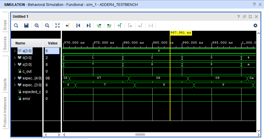
Figure 4.23 – Zoomed-in view of the simulation results
- Close simulation mode by clicking the X in the blue SIMULATION bar above the data trace window. Click OK when asked if you want to close the simulation.
Having passed behavioral testing, we will define the I/O signals used in the design.
Defining I/O signals
Our next step is to connect the inputs and outputs of our circuit to hardware devices on the Arty board. The inputs will be the board switches and pushbuttons, and the outputs will be LEDs.
The following steps will create a constraints file that describes the I/O pins we will use on the FPGA device and the functions connected to those pins on the Arty board. Constraint files have the xdc extension:
- In the Sources sub-window, right-click Constraints and select Add Sources….
- In the Add Sources dialog, ensure Add or create constraints is selected, then click Next.
- In the Add or Create Constraints dialog, click Create File.
- Enter the filename Arty-A7-100.xdc (or Arty-A7-35.xdc if appropriate for your device) and click OK.
- Click Finish to dismiss the Add or Create Constraints dialog.
- Expand the Constraints source tree and double-click Arty-A7-35.xdc.
- Digilent provides pre-populated constraint files for the Arty A7 boards online. Visit https://raw.githubusercontent.com/Digilent/digilent-xdc/master/Arty-A7-35-Master.xdc and copy the entire content of the browser window into the Arty-A7-35.xdc editor window in Vivado. If appropriate for your device, use the file at https://raw.githubusercontent.com/Digilent/digilent-xdc/master/Arty-A7-100-Master.xdc instead.
- All of the I/O pins are commented out in the constraints file by default. Uncomment the appropriate lines in the file by removing the # character from the beginning of each line. We will be using the pins listed in the following sections in the Arty-A7-100.xdc file: Switches, RGB LEDs (but only led0_g, the first green LED), LEDs, and Buttons. The following figure shows these lines after they have been uncommented:
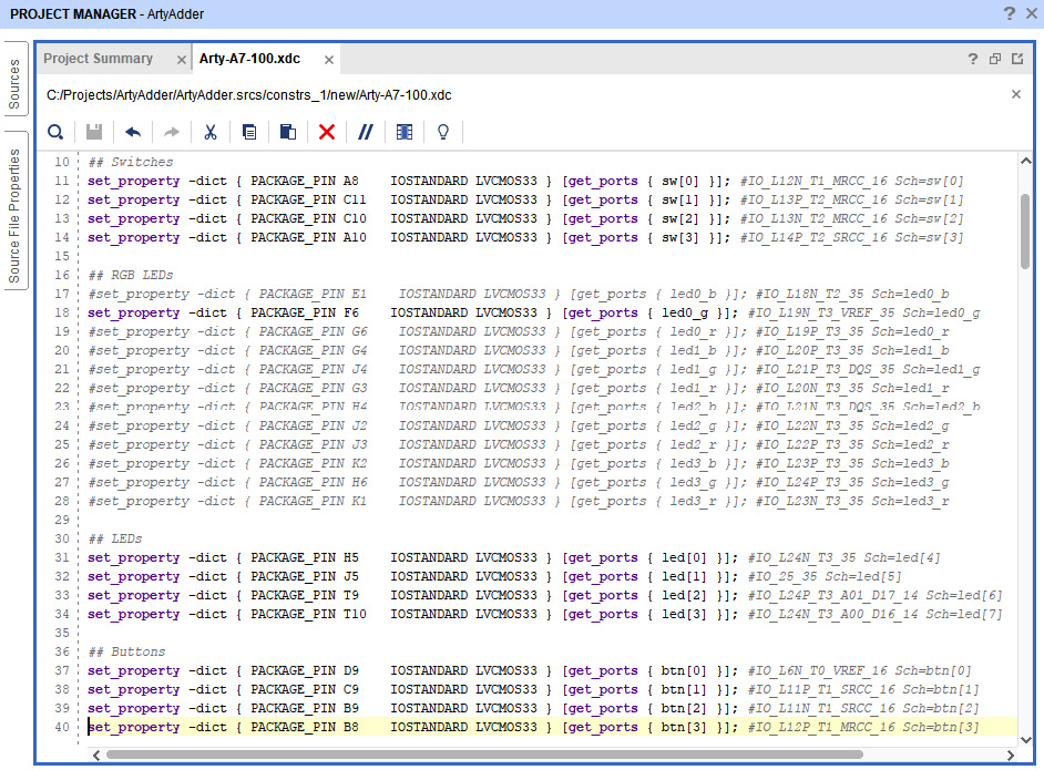
Figure 4.24 – Constraints editor window
In the next section, we will create a top-level VHDL file that interfaces the adder code with the I/O devices.
Creating a top-level VHDL file
We will next create a top-level VHDL file that connects our 4-bit adder component to the corresponding board I/O signals:
- In the Sources sub-window, right-click on Design Sources and select Add Sources….
- In the Add Sources dialog, ensure Add or create design sources is selected, then click Next.
- In the Add or Create Design Sources dialog, click Create File.
- Enter the filename ArtyAdder.vhdl and click OK.
- Click Finish to dismiss the Add or Create Design Sources dialog, then click OK in the Define Module dialog and click Yes when asked if you are sure you want to use these values.
- Double-click ArtyAdder.vhdl under Design Sources. Delete the automatically populated contents of the ArtyAdder.vhdl editor window and enter the following code into the ArtyAdder.vhdl editor:
-- Load the standard libraries
library IEEE;
use IEEE.STD_LOGIC_1164.ALL;
entity ARTY_ADDER is
port (
sw : in STD_LOGIC_VECTOR (3 downto 0);
btn : in STD_LOGIC_VECTOR (3 downto 0);
led : out STD_LOGIC_VECTOR (3 downto 0);
led0_g : out STD_LOGIC
);
end entity ARTY_ADDER;
architecture BEHAVIORAL of ARTY_ADDER is
-- Reference the previous definition of the 4-bit adder
component ADDER4 is
port (
A4 : in std_logic_vector(3 downto 0);
B4 : in std_logic_vector(3 downto 0);
SUM4 : out std_logic_vector(3 downto 0);
C_OUT4 : out std_logic
);
end component;
begin
ADDER : ADDER4
port map (
A4 => sw,
B4 => btn,
SUM4 => led,
C_OUT4 => led0_g
);
end architecture BEHAVIORAL;
This code maps the signal names for the I/O devices named in Arty-A7-100.xdc as sw (4 switches), btn (4 pushbuttons), led (4 single-color LEDs), and led0_g (the green channel of the first multi-color LED) to the ADDER4 inputs and outputs.
While VHDL is not case-sensitive, the processing of xdc constraint files in Vivado is case-sensitive. The case used in I/O device names defined in the xdc file must be identical when referenced in a VHDL file. Specifically, the I/O signal names in VHDL must be lowercase in this file because they are lowercase in the constraints file.
We are now ready to synthesize, implement, and program our design for the Arty board.
Synthesizing and implementing the FPGA bitstream
If you wish, you can separately perform the synthesis and the implementation (place and route) steps using the selections in the Flow Navigator portion of the Vivado main dialog.
Alternatively, you can select Generate Bitstream and Vivado will perform all of the required steps, including synthesis, implementation, and bitstream generation without further user intervention. If a fatal error occurs, the process will stop and error messages will be displayed. Perform the following steps to generate the bitstream:
- Click Generate Bitstream to start the build process. You may be asked if you want to save text editors. Click Save. You may be informed that there are no implementation results available and asked if it is OK to launch synthesis and implementation. Click Yes:

Figure 4.25 – Generate Bitstream menu selection
- The Launch Runs dialog will then appear. You can select a value for Number of jobs up to the number of processor cores in your computer. Using more cores makes the process go faster, but it can bog down your machine if you want to continue using it during a lengthy build process. Click OK to start the build:

Figure 4.26 – Launch Runs dialog
- During the build process, Vivado will display the status in the upper-right corner of the main window. If necessary, you can cancel the build process by clicking Cancel next to the status display:

Figure 4.27 – Compilation status display
- When the build process completes, assuming there were no fatal errors, a Bitstream Generation Completed dialog will appear. Although other options are offered, we will proceed directly to downloading the bitstream to the Arty board. Select Open Hardware Manager and click OK:
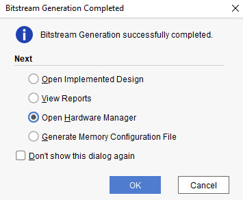
Figure 4.28 – Bitstream Generation Completed dialog
Next, we will download the bitstream into the FPGA.
Downloading the bitstream to the board
Perform the following steps to download the bitstream to an Arty A7 board:
- The HARDWARE MANAGER dialog will appear and indicate No hardware target is open.
- Connect your Arty A7-35 or A7-100 board to the computer with a USB cable. Wait a few seconds for the board to be recognized, then click Open target, then Auto Connect:
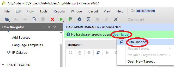
Figure 4.29 – Open target and Auto Connect selections
- After a few seconds, Vivado should indicate that the board is connected. Click Program device to download the FPGA bitstream to the Arty board. You will be prompted to select a bitstream file. If you've used the same directory structure as this example, the file will be located at C:/Projects/ArtyAdder/ArtyAdder.runs/impl_1/ARTY_ADDER.bit:
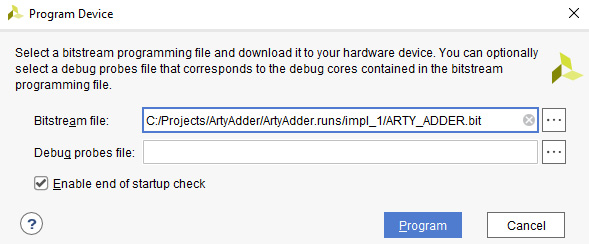
Figure 4.30 – Program Device dialog
- Click Program to download the program to the FPGA device and start it executing.
- You can now test the operation of the program with the Arty I/O devices. Place all of the four switches in the off position (move the switches toward the adjacent board edge) and do not press any of the four pushbuttons. All of the four green LEDs should be off.
- If you turn on any individual switch or press any one pushbutton, the corresponding green LED should turn on. Turning on any combination of switches while pressing any number of pushbuttons will add the corresponding 4-bit numbers and light the LEDs with the result. If there is a carry (for example, turn on SW3 and press BTN3 simultaneously), the green carry LED will illuminate.
The programming process performed here stored the program in FPGA RAM. If you cycle power on the FPGA board, you will need to repeat the programming process to reload the program. Alternatively, you can store the FPGA configuration file in onboard flash memory as described in the following section.
Programming the bitstream to onboard flash memory
To configure the FPGA each time power is applied to the Arty board, the FPGA configuration file must be stored to flash memory on the board. If the MODE jumper is installed, the FPGA will attempt to download a configuration file from onboard flash memory at power-on. This memory is located in a separate chip adjacent to the Artix-7 FPGA. Follow these steps to program the configuration file to flash memory:
- Install the MODE jumper on the Arty board if it is not already in place.
- Right-click Generate Bitstream and select Bitstream Settings….
- In the Settings dialog, check the box next to -bin_file and click OK:
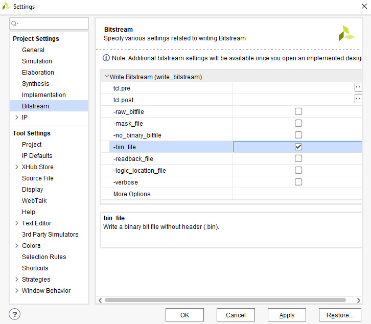
Figure 4.31 – Bitstream settings dialog
- In the main Vivado dialog, click Generate Bitstream and repeat the bitstream generation process. Click Cancel when the Bitstream Generation Completed dialog appears.
- In the Hardware dialog, right-click the FPGA part number (xc7a100t_0) and select Add Configuration Memory Device…:

Figure 4.32 – Add Configuration Memory Device… menu selection
- Type s25fl127 into the Search box. This should bring up one matching part number. Select the part and click OK:
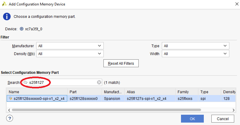
Figure 4.33 – Add Configuration Memory Device dialog
- You will be presented with a dialog asking Do you want to program the configuration memory device now? Click OK.
- This will bring up a Program Configuration Memory Device dialog requesting the configuration filename. Click the … button to the right of Configuration file and select C:/Projects/ArtyAdder/ArtyAdder.runs/impl_1/ARTY_ADDER.bin. Click OK:

Figure 4.34 – Program Configuration Memory Device dialog
- The programming process will take several seconds to complete. You should receive a message indicating success after the file has been programmed into the board flash memory:
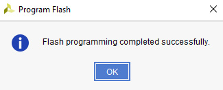
Figure 4.35 – Program Flash complete dialog
After this, each time you cycle the board power, the 4-bit adder program will load and run. It will take a long time for the program to load with the settings that we used for configuration file loading. To avoid waiting for the FPGA to load the program, you can improve the speed of configuration file loading by performing the following steps:
- Select Open Synthesized Design in Flow Navigator.
- In the Vivado main menu, select Tools/Edit Device Properties….
- In the General tab, set Enable Bitstream Compression to TRUE.
- In the Configuration tab, set Configuration Rate (MHz) to 33, then click OK.
- Generate the bitstream again, and program the flash memory as described previously. You will need to remove the configuration memory device and add it back again to display the option for reprogramming.
- Close Hardware Manager.
- Unplug the Arty board USB cable and plug it in again. The program should begin running virtually instantaneously at power-on.
This section presented an example of simple combinational logic interacting with signals on the FPGA I/O pins. The intent here has been to familiarize you with the Vivado tool suite and to demonstrate how the tools are used to perform a complete FPGA development cycle.
Summary
This chapter began with a discussion on the effective use of FPGAs in real-time embedded system architectures and continued with a description of standard FPGA devices and the low-level components they contain. The range of FPGA design languages, including HDLs, block diagram methods, and popular software programming languages such as C/C++, was introduced. An outline of the FPGA development process was presented. The chapter concluded with a complete example of an FPGA development cycle, starting with a statement of requirements and ending with a functional system implemented on a low-cost FPGA development board.
Having completed this chapter, you should know how FPGAs can be applied effectively in real-time embedded system architectures and understand the components inside an FPGA integrated circuit. You have learned about the programming languages used in the design of FPGA algorithms, the steps in the FPGA development cycle, and understand the sequence of steps in the FPGA development process.
The next chapter will expand on the FPGA development process to provide a complete approach to architecting real-time embedded systems containing FPGAs. It will also begin the development of a prototype high-performance embedded system, a digital oscilloscope, that will serve as an example for the following chapters.