
Interfacing Between an ESS and a Microgrid
This chapter discusses the interfacing circuits needed for an energy storage system (ESS) to connect to the microgrid. In the first part, the structures and basic principles of several power converters are discussed. They include DC-DC converters, AC-DC rectifiers, DC-AC inverters, AC-AC converters. The most important DC-DC converter for an ESS is the bidirectional buck-boost DC-DC converter, which can help the ESS to be charged and discharged. For DC-AC converters, the voltage source inverter (VSI) is the most used converter in practice. A VSI can be used to integrate an ESS or solar photovoltaic into the microgrid. The following section introduces battery management systems (BMS). The different configurations of BMS are given. Within a BMS, cell balancing is important for reliable operation of the battery energy storage systems (ESS). Thus, two different cell-balancing functions of BMS are presented, namely active cell balancing and passive cell balancing. Two case studies are presented in the last section. The first case is about the control of bidirectional DC-DC converter; the second case is the dq control of VSI. The results show that real power and reactive power are controlled independently.
Keywords
DC-DC converter; AC-DC converter; DC-AC converter; voltage source inverter; battery management system; dq control
3.1 Introduction
Power converter interface devices are important for using energy storage systems (ESSs) in microgrids. With the development of power electronics technology, many different power converters have emerged, which make the charging and discharging process of ESS controllable due to the bidirectional power flow ability of some converters.
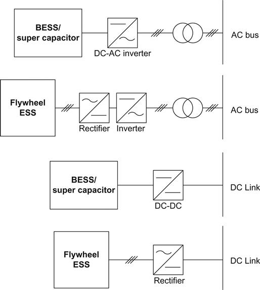
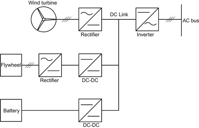
Figure 3.1 shows some applications of power electronic converters for ESSs in microgrids, which may have a common DC and AC bus. The converter may differ for different ESSs, for example, a battery energy storage system (BESS) needs DC-DC or DC-AC converters to connect to a microgrid and for a flywheel energy storage system (FESS), a back-to-back converter is needed to perform AC-AC conversion; or a rectifier can be used to convert AC output power from FESS to DC to connect to a DC link in a microgrid.
In this chapter, several different power converters are discussed including DC-DC converters, AC-DC rectifiers, DC-AC inverters, and AC-AC converters. The structures and the principles of these converters are presented in the next sections.
In addition to converters, the management system is also essential for an ESS in a microgrid. The management system handles the operation of ESS, especially the charging and discharging process. In this chapter, the battery management system (BMS) is introduced. One major feature of the BMS is cell balancing of the battery package.
At the last part of this chapter, some applications of converters for ESS are presented with some specific control strategies.
3.2 DC-DC Converter
DC-DC converters are used to change the voltage level at the DC source input to the desired DC output voltage level. There are several different types of DC-DC converters, namely step-down converter, step-up converter, and bidirectional DC-DC converter. A step-down converter converts a high voltage DC source into a low voltage output, while a step-up converter increases the DC source voltage to a higher output voltage. The bidirectional DC-DC converter can do both step-down and step-up conversions, and the power can flow in either direction between input and output.
Many ESSs are DC power sources, e.g., batteries and supercapacitors. Also, the DC link appears in microgrids in between back-to-back converters. So, a DC-DC converter can connect DC ESSs to the DC link in a microgrid. In addition, for a photovoltaic (PV) microgrid, the ESS can work to mitigate the intermittency of the PV output through control of DC-DC converter.
In this section, several DC-DC converters will be introduced. They cover the categories of step-down converter, step-up converter and bidirectional DC-DC converter.
3.2.1 Buck Converter (Step-Down Converter)
Buck converter is a simple and widely used voltage step-down device with high efficiency (e.g., 95% or above). Figure 3.2 shows a typical circuit of a buck converter.
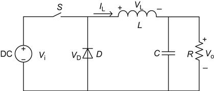
In the buck converter, the inductor plays a major role to lower the input voltage. There are two states in the operation process of buck converter: the on-state and off-state of the switch S. During the on-state, the control signal closes the switch S. Since the source Vi is serially connected to the inductor and load, the current IL through the inductor L is increasing. According to Faraday’s law of induction, there will be a voltage VL induced across the inductor. This opposing voltage VL counteracts the voltage of the source and reduces the voltage on the load. At the same time, the inductor absorbs energy from the source and stores the energy in the form of a magnetic field.
On the other hand, if the switch S is opened by a control signal, this results in the off-state of the converter. In the off-state, the source voltage Vi is disconnected from the circuit by the switch. Due to the diode D, the current IL through the inductor will continue to flow but its magnitude will drop. As a result, the induced voltage across the inductor will change its direction. Since there is energy stored in the inductor, the inductor becomes a source to supply the load by releasing its stored energy.
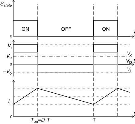
By switching between on-state and off-state constantly, the buck converter is able to decrease the voltage from the input to the output. If the current through the inductor never falls to zero during the whole process, the converter is said to be in continuous mode. Otherwise, it is in discontinuous mode. Figure 3.3 shows the current and voltage change during the continuous mode.
The voltage across the inductor is related to the change rate of its current, as given in Eq. (3.1).
(3.1)
Therefore, in continuous mode, the change of current can be calculated for both on-state and off-state. Equation (3.2) denotes the current change in on-state.
(3.2)
Similarly, for the off-state, the decrease of current through the inductor is computed by Eq. (3.3)
(3.3)
If the converter operates in a steady state, during a cycle, the current through the inductor at the beginning of the on-state will be the same as the current at the end of the off-state. This means that the accumulated current change during one operational cycle (i.e., one period consisting of one on-state and one off-state) is zero.
(3.4)
Let ![]() be the switch duty cycle, and 0<D<1. Equation (3.4) becomes:
be the switch duty cycle, and 0<D<1. Equation (3.4) becomes:
(3.5)
(3.6)
So, by controlling the switch duty cycle of the converter, the output voltage Vo can be controlled. Also, as D is always blow 1, Eq. (3.6) shows that the output voltage is always lower than the input voltage.
3.2.2 Boost Converter (Step-Up Converter)
Like the buck converter, the boost converter has a simple structure, as shown in Figure 3.4. The function of a boost converter is to increase the input voltage to a higher output voltage. Again, the inductor in the circuit plays a major role to boost the input voltage.
The boost converter also has an on-state and an off-state. In the on-state, the switch S is in closed position, ID=0, the current IL through the inductor L is increasing and the voltage across the inductor is equal to the source voltage. In this process, the inductor is storing energy from the source.
In the off-state, the switch is open. The load is reconnected to the source and the inductor. Hence, the current through the inductor will decrease, resulting in an induced voltage across inductor in the same direction of the source voltage. Now, the inductor becomes another source to supply the load by releasing its stored energy. Since the source and inductor are connected in series, the voltage on the load is the aggregation of the voltage on inductor and source voltage, which means the output voltage is higher than the source.
(3.7)
If the current through the inductor is always above zero, the converter is working in continuous mode. According to the relationship between the current and voltage of the inductor, the change of current during on-state and off-state can be obtained. In the on-state, only the source Vi influences the current through the inductor as Eq. (3.8) shows.
(3.8)
where D is the duty cycle. In the off-state, both the source and the load are connected with the inductor in series. The inductor current change is given in Eq. (3.9).
(3.9)
In the steady state, as Figure 3.5 shows, the current IL at the beginning of on-state and at the end of the off-state will be the same, which means that the accumulated current change during a cycle is zero. Therefore, the following relationship of the current change through the inductor can be obtained:
(3.10)
which implies that
(3.11)

Because the duty cycle D is less than 1, the ratio in Eq. (3.11) will always be bigger than 1. This implies that the output voltage Vo is always higher than the input Vi. The gain of the boost converter can be controlled by the duty cycle D.
3.2.3 Bidirectional Buck-Boost Converter
In a microgrid system, charging and discharging of BESS requires the DC-DC converter to be bidirectional so that the power flow can change direction between the ESS and the microgrid. Typically, the voltage at the ESS side is lower than that at the microgrid side. That means that the ESS voltage must be stepped up so that the ESS can discharge to supply power to the microgrid. Conversely, when the ESS is being charged, the higher voltage at the DC-bus of the microgrid needs to be stepped down to the rated voltage of the ESS.
Figure 3.6 shows the structure of a bidirectional DC-DC converter. The transistors in the converter work as switches to connect or disconnect the circuit. This bidirectional DC-DC converter can be considered as a combination of a buck converter and a boost converter. In the buck converter mode, the transistor T1 is always off, current flows from the DC-bus to the ESS source. By controlling the transistor T2, the converter can decrease the microgrid side voltage VDC to charge the ESS. If the converter works in boost converter mode, the transistor T2 is always in its off-state and the diode on T2 facilitates current flow in one direction from the ESS source to the microgrid. By controlling the duty cycle D of the transistor T1, the converter is able to increase the output voltage VESS of the ESS so as to supply power to the microgrid.

A case study of bidirectional buck-boost converter will be given at the end of this chapter.
3.3 AC-DC and DC-AC Converter
AC-DC converters are also called rectifiers, which is a device to convert AC power into DC output. In a power system, three-phase rectifiers are very important for industrial applications and for the transmission of energy, e.g., in High Voltage Direct Current (HVDC) transmission system. In microgrids, the rectifier is useful to provide DC power to charge the ESS.
On the other hand, DC-AC converters are also called inverters, and are very important devices in power systems. For any DC power source, an inverter is needed to connect to an AC bus.
The structures of typical inverters and rectifiers are similar, which make it possible for a converter to function as either a rectifier or an inverter. For example, a voltage source converter (VSC) can be controlled to function as rectifier or inverter and allows bidirectional power flow.
In this section, different AC-DC rectifiers and DC-AC inverters will be introduced.
3.3.1 Single-Phase AC-DC Rectifier
In a single-phase rectifier, the input of the rectifier is one phase AC power. There are two major AC-DC rectifier types: half-wave rectifier and full-wave rectifier. The structures of these two types of rectifiers are very simple and no control signal is required.
3.3.1.1 Single-Phase Half-Wave Rectifier
This half-wave rectifier can have the simplest structure among all the AC-DC converters. As shown in Figure 3.7, only one diode D is needed in the half-wave rectifier. This diode limits the current flow in one direction. This means that only half of the AC waveform can pass through the diode, as shown in Figure 3.8.
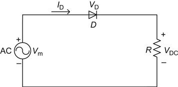

The input and output voltage waveforms of an example rectifier with a resistive load are shown in Figure 3.8. In the diagram, only the positive part of the input waveform does useful work. Thus the efficiency of the half-wave rectifier is very low.
According to the waveform in Figure 3.8, the voltage relationship of the input and output can be calculated. The average voltage on the load is:
(3.12)
 (3.12)
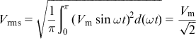
where Vm denotes the amplitude of the input voltage. Further, the root-mean-square (rms) value of load voltage is:
(3.13)
 (3.13)
Note that the output of the rectifier is half of the AC voltage source, which is not constant. Therefore, in many applications, a filter is needed to convert the half-wave DC voltage into a constant DC voltage.
3.3.1.2 Single-Phase Full-Wave Rectifier
Differing from the half-wave rectifier, the full-wave rectifier allows the input AC source to complete its current flow circuit in both positive and negative half of an AC cycle. The structure of the full-wave rectifier is shown in Figure 3.9.
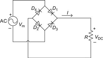
There are four diodes in the full-wave rectifier circuit. When the AC source voltage is positive, the current flows through D1 to the load and back to the AC source via D2. When the AC source voltage is negative, the current flows via D3-load-D4 path. Either way, the current always goes across the load from the positive to the negative pole.
Figure 3.10 shows the waveforms of the input and output voltage of the full-wave rectifier. It can be considered as if rectifier flips the negative voltage to the positive side. Thus, the period of the waveform changes from 2π to π. Therefore, the average voltage across the load can be calculated as in Eq. (3.14).
(3.14)

And the rms value of load voltage is:
(3.15)
 (3.15)
Compared with the half-wave rectifier, the average voltage for the full-wave rectifier is twice that of the half-wave rectifier’s average voltage. The output rms voltage of full-wave rectifier is ![]() times higher than that of half-wave rectifier.
times higher than that of half-wave rectifier.
3.3.2 Three-Phase AC-DC Rectifier
3.3.2.1 Three-Phase Half-Wave Rectifier
The star rectifier is a commonly used three-phase half-wave rectifier, which is like an aggregation of three single-phase half-wave rectifiers. The star rectifier can be more than three-phase by adding more diodes. Figure 3.11 shows the structure of a controllable three-phase half-wave rectifier. Each phase has a similar structure to one single-phase half-wave rectifier, and they are connected in parallel with each other. The diode’s thyristors can be controlled to turn on or off at different times to produce different DC output voltages.
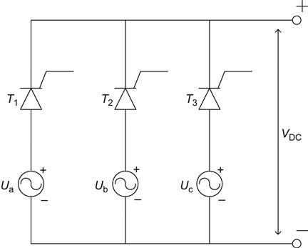
For the three-phase half-wave rectifier, if the control signal is always on for the thyristors, the three thyristors will work as normal diodes. Because the diode conducts only if the anode-to-cathode voltage is positive, the output voltage VDC is in phase with highest voltage envelope, as shown in Figure 3.12.
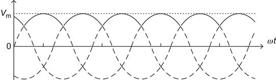
Besides the always-on mode, the control signal can make the thyristors conduct with a delay angle α for each phase. Assuming that the delay is counted from the crossing point between two phase voltages, the waveform of the output voltage for a resistive load looks like the form in Figure 3.13.

According to Figure 3.13, the output voltage has a period of ![]() . The average voltage on the resistive load can be calculated from:
. The average voltage on the resistive load can be calculated from:
(3.16)
Because ![]() for the input AC source voltage then,
for the input AC source voltage then,
(3.17)
From Eq. (3.17), it is clear that the output of the star rectifier has the highest magnitude when the delay α=0°.
3.3.2.2 Three-Phase Full-Wave Rectifier
The three-phase full-wave rectifier has the bridge structure as shown in Figure 3.14. If all six thyristors are controllable, it is known as a fully controllable bridge converter. However, if the thyristors always conduct like diodes, the operation principle of the rectifier is similar to the single-phase full-wave rectifier discussed in preceding sections. This means that the negative half cycle voltage of each phase will flip to the positive side.
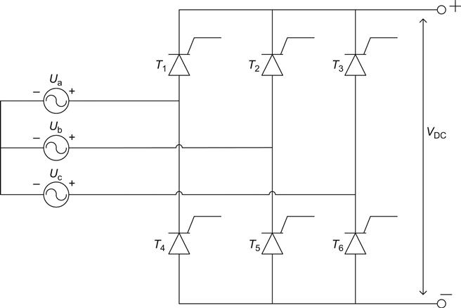
By introducing the delay angle α to the control signals, the output voltage can be controlled like the three-phase half-wave rectifier. Equation (3.18) shows the calculation of the average voltage on the DC side.
(3.18)
In a similar manner to the three-phase half-wave rectifier, the maximum output voltage happens when the delay α=0°.
For normal rectification applications, there is no need to control all the thyristors in the bridge. So the circuit can be simplified into a half controlled rectifier, as shown in Figure 3.15. In the half controlled bridge structure, the three thyristors, T4, T5, and T6, can be replaced by diodes. By controlling the other three thyristors (T1, T2, and T3), the rectifier can still achieve the desire performance. Since the diode is cheaper than thyristor, the half controlled bridge structure is cheaper.

3.3.3 Single-Phase DC-AC Inverter
The single-phase DC-AC inverter can convert DC input voltage into single-phase AC output voltage. Figure 3.16 shows the circuit of a single-phase DC-AC inverter. The circuit is an H-bridge structure with four controllable transistors.
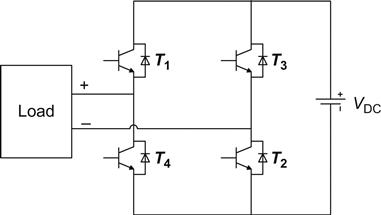
A simple way to generate AC voltage on the load is called the Bipolar pulse width modulation (PWM) Technique [1]. In this method, the controller sends signal to turn on T1 and T2 during 0<t<T/2, which results in a positive current flow across the load. When T/2<t<T, the controller turns off T1 and T2 and switches on T3 and T4, so the current through the load becomes negative. By switching between these two modes continuously, an AC voltage (square wave) with period T can be obtained across the load. In order to obtain sinusoidal AC output voltage, a filter is needed to remove the harmonics.
Note that T1 and T4 (or T2 and T3) should not conduct at the same time, otherwise the DC side will be shorted.
3.3.4 Voltage Source DC-AC Inverter
Today, most microgrids work in a three-phase AC power environment just like the traditional grid. In many applications, the ESS needs to connect to the AC bus in the microgrid. So a three-phase inverter is required. The structure of a three-phase inverter is similar to a controllable three-phase rectifier, thus many inverters are bidirectional and can work in DC-AC inverter or AC-DC rectifier mode.
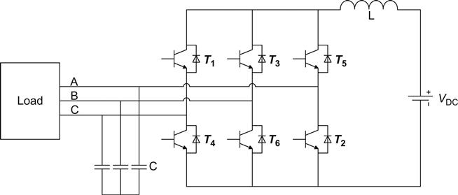
The voltage source inverter (VSI) is a commonly used power inverter. It converts a DC voltage into a three-phase AC voltage. The structure of a three-phase VSI is illustrated in Figure 3.17. The three-phase VSI has six transistors to form a bridge structure with three legs.

The basic control scheme of VSI can be achieved by operating three transistor pairs coordinately, through a six-step sequencing control. The switches on the same branch (e.g., T1 and T4) are controlled by opposite signals so that they cannot conduct simultaneously, otherwise the DC source will be shorted by this branch. The six-step sequencing control is shown in Figure 3.18.
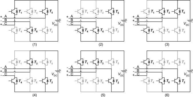
The control scheme contains six steps, and the duration of each step is π/3. At each step, the transistor pair on one branch switch their signals, but the other two branches do not change. The three-phase output voltage waveforms of the VSI with six-step sequencing control are shown in Figure 3.19.

There are many applications of VSIs in microgrids. One of the most important application is as a solar PV power inverter. Companies like Fronius, Outback and SMA, sell many types of PV inverters for different ratings. In many of their products, the PV inverter not only converts the DC power from PV panels into AC output but also is equipped with some advanced features like Maximum Power Point Tracking (MPPT). Figure 3.20 shows PV inverter products from different companies.

3.3.5 Current Source DC-AC Inverter
The current source inverter (CSI) is another type of inverter. Different from VSI, the CSI converts DC current into an AC current. Figure 3.21 shows the structure of a CSI. It is clear that CSIs have similar structures to VSIs. But, in order to mitigate the high current variation in CSI, capacitors are usually installed on the AC side, while inductor is employed on the DC side.
3.4 AC-AC Converter and Transformer
AC-AC converters and transformers are also important converters for renewable microgrids and ESSs. In the renewable microgrid, some Distributed Generators (DGs) have AC power output, e.g., wind turbines and hydro generators. For ESS, the flywheel is an important AC storage system. Therefore, AC-AC converters and transformers can be used to control the output of renewables and the charging/discharging process of ESS. In addition, AC-AC converters and transformers can be employed to isolate the power source from the AC bus of the microgrid. For AC-AC converters, the DC link can separate the AC lines so that the effects of undesired harmonics caused by renewables can be reduced. By installing transformers, galvanic isolation can be achieved. Hence, the AC-AC converter and transformer can help to improve the stability of a microgrid.
3.4.1 Back-to-Back Converter
For renewables and ESS, a back-to-back structure is often used in the AC-AC converter. The charging and discharging of a FESS is usually controlled by a back-to-back converter. The back-to-back converter can control the input and output AC power with its transistors or Insulated-gate bipolar transistor (IGBT) switches. Figure 3.22 shows a typical back-to-back AC-AC converter, which is a combination of two VSCs with a DC link in between. So the back-to-back AC-AC converter can be controlled as two separate converters.

For example, in a FESS [2], the back-to-back converter absorbs energy from the AC bus to charge the FESS. The VSC2 on the grid side works as a rectifier to convert the AC power into stable DC power with constant voltage VDC on the DC link. The controller for VSC2 can be designed as dual-loop controller with an inner current control and an outer voltage control loop. Meanwhile, the VSC1 works in inverter mode to convert the stabilized DC voltage into AC to supply the FESS. The VSC1 also has a dual-loop controller, which controls the current and speed of the flywheel’s permanent magnet brushless DC machine (BLDCM).
In the discharging process, the VSC1 and VSC2 switch their operation modes. However, since the output of flywheel decreases when discharging, the VSC1 should be a boost rectifier with current-voltage dual-loop controller [3]. For VSC2, it works as an inverter to convert the DC power into stable AC power to supply the microgrid.
An application example of a back-to-back converter is the FESS based Power Control Module (PCM) of Beacon Power Company, as shown in Figure 3.23.

The PCM can help the flywheel ESS to couple with the microgrid. The AFE (Active Front End) in the PCM can work as an active rectifier that converts line frequency AC power into DC, while the FWC (Flywheel Controller) of the converter inverts DC power into adjustable voltage and adjustable frequency AC for the flywheel. The PCM has been implemented in some projects, such as Energy Storage Pilot Project—Tyngsboro and Hazle Township project [4].
3.4.2 Transformer
Transformers are the most commonly used AC-AC converter device in power systems. But as opposed to power electronic converters, most transformers are uncontrollable, with a fixed conversion ratio. However, the transformer can be used in microgrids for galvanic isolation and to further step-up or step-down the AC voltage.
In Figure 3.24, example applications of transformers in microgrids with renewables and ESS are presented. It can be seen from the figure that the transformers can work with the inverters to interface with the AC bus. So the AC bus of the microgrid can be isolated from the renewables and ESS.

3.5 Battery Management System
BESS is one of the most applied energy storage technologies. Due to the fast response and high energy density of batteries, they have been widely applied in many microgrid projects.
In a BESS, hundreds of batteries work together to provide enough energy for the microgrid. Therefore, a BMS is required to coordinate the operation of all the batteries. The objective of the BMS is to provide protection, increase the life-span and maintain the stability of the batteries in the BESS. In order to accomplish the tasks, the BMS should have the functions of monitoring, computation, control and communication.
To protect the batteries from damage and maintain them in good condition, the BMS needs to monitor the temperature, voltage and current in the batteries. Overheating the battery is very dangerous, and may lead to explosion and fire. Hence, temperature monitoring is very important to ensure that the batteries work in stable conditions. The voltage information of the battery indicates its state, which is useful to identify the state-of-charge (SOC) of the batteries, so that overcharging or over-discharging can be prevented. Furthermore, the current of batteries should stay in a safe range, especially during the charging process. If the charging current is too high, it will not only damage the battery’s health, but also causes accidents. However, if the charging current is too low, it will take a very long time to fully charge the battery.
The BMS also needs to perform many computations. For example, the SOC and state-of-health of the batteries should be calculated based on the voltage and current information.
In addition to charging and discharging control process of each battery, the SOC of each battery needs to be balanced. For charging and discharging control, the BMS should cooperate with the DC-DC converter to have the desired charging current.
For many control strategies, operation of the BESS is coordinated with other sources to achieve the optimal operation of the microgrid. So, the BMS needs to communicate with other devices in the microgrid. In a microgrid with multi-level control structure, the BMS will communicate with the central controller to report the conditions of batteries and receive control tasks.
There are two major topologies of BMS: centralized BMS and master-slave BMS. In this section, these two architectures will be introduced. Then the cell balancing technology will be presented.
3.5.1 Centralized BMS
Centralized BMS architecture has one central BMS in the BESS. All the battery packages are connected to the central BMS directly. The structure of a centralized BMS is shown in Figure 3.25.
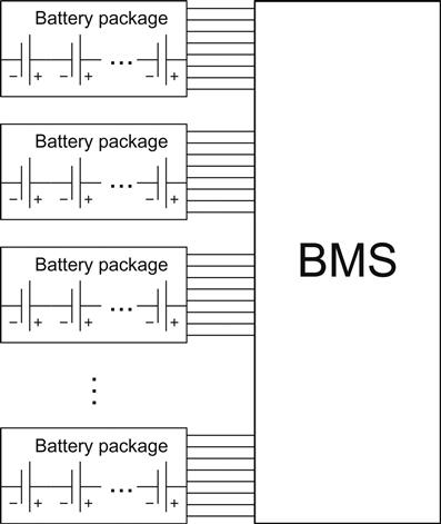
The centralized BMS has some advantages. First, it is more compact. Second, the centralized BMS solution is the most economical since there is only one BMS. However, the disadvantages of centralized BMS are obvious. As all the batteries should be connected to the BMS directly, the BMS needs a lot of ports to connect with all the battery packages. However, there are too many wires in the BESS, making maintenance difficult. Therefore, if the BESS contains a lot of battery packages, a centralized BMS is not a good option.
3.5.2 Master-Slave BMS
The master-slave BMS has a different structure from the centralized BMS, as shown in Figure 3.26. In the master-slave BMS structure, there are two different types of BMS: the master BMS and the slave BMS.

For each battery package in the BESS, there is a slave BMS. The slave BMS controls the charging and discharging processes and monitors the conditions of each battery package. Also, it performs the cell balancing feature for its battery package. The master BMS assigns the tasks for each battery package and determines which battery packages should work. Moreover, the master BMS deals with communication between the BESS and the microgrid controller.
3.5.3 Cell Balancing
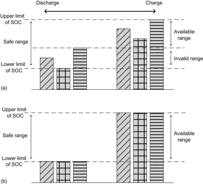
In each battery package, several battery cells are connected in series to achieve a bigger capacity. However, the quality or ability of each battery cell is not identical, which may result in imbalance among cells during charging or discharging.
The imbalance among battery cells will decrease the available energy of the overall battery package. As illustrated in Figure 3.27a, in which three cells are connected in series to form a battery package, there are two unbalanced states in which each cell has a different SOC. Due to the safe range requirement of the battery’s SOC, the battery package stops charging or discharging when one of the cells reaches the limits. Therefore, for the unbalanced situation, the battery package will not continue to charge or discharge when the battery cell with the highest SOC reaches the upper limit or the battery cell with lowest SOC reaches the lower limit. As a result, the cells within the battery package cannot be fully charged or fully discharged, except the battery cell with highest SOC or lowest SOC. Thus, the available range of SOC for charging or discharging is reduced. If the batteries are balanced, as shown in Figure 3.27b, all the battery cells can be charged and discharged fully, and the available range of battery package is maximized.
On the other hand, the parallel-connected battery cells can self-balance, so cell balancing is not needed in this structure. There are two different cell balancing techniques, passive cell balancing and active cell balancing.
3.5.3.1 Passive Cell Balancing
The commonly used passive cell balancing approach is known as “resistor bleeding balancing.” It uses a bypass circuits to balance each battery cell. The circuit for passive cell balancing is shown in Figure 3.28.

There are some field-effect transistors (FET) and resistors connected to each cell in parallel. The balancing process can happen during both charging and discharging periods. In the charging process, the BMS calculates the SOC for each battery cell and finds out the highest one (suppose it is Bi). Then, the BMS sends a signal to turn on Sia FET, and this will cause a current to flow through the resistor Ria. This current creates a voltage on resistor Ria to turn on the FET Sib. As a result, the charging current will not flow in battery Bi and bypass through the resistor Rib. For the discharging process, the BMS will also check the battery with highest SOC (Bi). By turning on Sia, the FET Sib will be turned on due to the same reason in charging process. So, the battery Bi will start to discharge as it is connected to resistor Rib.
After performing the balancing process for a while, all the battery cells in the battery package will have the same SOC. However, as the current is bypassed through the resistors, it is obvious that passive cell balancing is not energy efficient. The energy is wasted as heat on the resistors. Hence, passive cell balancing is not an efficient way to manage the batteries.
3.5.3.2 Active Cell Balancing
Time-shared cell balancing is a popular method to balance the battery cells in BESS. The circuit of time-shared active cell balancing is shown in Figure 3.29. BMS obtains the battery voltage through the cell selection switches (i.e., S2,1 and S2,2 for battery B2) and ADC (analog-digital converter) switch (Sa and Sb). Because the series-connected battery cells are at different voltage reference levels, the battery voltage can be obtained by a flying capacitor.
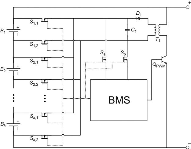
The operation process is as follows. When the BESS is at discharging mode, FETs Si and Si+1 makes a connection between one of the battery cells and the flying capacitor C1, and the battery voltage is transferred to the flying capacitor. Hence, the connection status is changed from (Si, Si+1) to (Sa, Sb) and the BMS reads the voltage of the flying capacitor. These switches are sequentially turned on from the first battery cell to the last one. Therefore, by calculating the SOC with this voltage information, the battery cell with the lowest SOC can be located. In this state, the PWM switch (QPWM) for DC/DC converter is not operated.
Suppose the battery with the lowest SOC is Bi. When battery cells are being charged from the microgrid, FETs Si,1 and Si,2 connect the battery Bi to the transformer T1. The BMS controls the FET QPWM with PWM signal to transfer the current from input through the transformer T1. So the battery cell Bi can be charged directly by the transformer. This process is continued until all the battery cells have the same SOC and thus the cell balancing is achieved.
3.6 Applications of Converters for ESS in Microgrid
In this section, several applications of converters for ESS will be introduced including the application of DC-DC converter to integrate ESS with renewables and the dq decoupled control for inverter.
3.6.1 ESS Integration with Renewables
Currently, renewable energy generation is the major power source of many microgrids. Since the outputs of many renewable energy sources are intermittent, ESS can work with renewables to improve their power quality. In many applications, the ESS is connected to the DC link, as shown in Figure 3.30. The DC link is a bus located behind the inverter, which is connected to the AC bus of the microgrid. The DC link is important to isolate the power source from the grid and improve the power quality since the output of generator may contain undesired harmonics [5].

Suppose that the ESS output is DC power, e.g., from BESS, the bidirectional buck-boost converter can be installed within the ESS in order to charge and discharge the ESS. If the output of ESS is AC, e.g., FESS, it can be rectified into DC power at first, and then connected to the bidirectional DC-DC converter. In Figure 3.31, these two types of structures are illustrated. Note that the rectifier connecting the FESS to the DC-DC converter should be bidirectional, which can be implemented with a VSC.
The function of the bidirectional DC-DC converter is to control the charging and discharging process of the ESS. Proportional-integral (PI) control is the common control strategy for this application. The controller should generate appropriate gate signal for the power electronic switches in the bidirectional DC-DC converter so that the output voltage or input current is able to arrive at desired value. An example controller structure is presented in Figure 3.32.
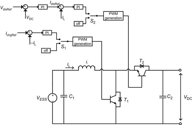
When the ESS is discharging, the control system changes S1 to the off position and S2 to the upper position to activate the discharging controller. Hence, the bidirectional DC-DC converter is working in boost converter mode to increase the output voltage of ESS to match the voltage on DC link. The discharging controller is a voltage-current dual-loop controller; the inner loop is a current loop to stabilize the discharging current through the inductor L, while the outer voltage loop controls the output voltage of the converter. The output of the outer controller is connected to a PWM generation module, which converts the control signal into the PWM gate signal for the transistor T2.
In the charging process, the control system changes the position of switch S1 to connect to the charging controller and turns S2 to the off position. Thus, the converter works in buck converter mode and it decreases the voltage on the DC link to charge the ESS with desired current. If the charging current is too high or too low, it is bad for the health of the battery. Therefore, the reference of the charging controller, IchgRef, is the desired charging current. The error between the reference and the actual charging current is input to a PI controller. Like in the discharging controller, a PWM generation module converts the control signal from the PI controller into a PWM gate signal and sends it to the transistor T1.
3.6.2 dq Decoupling Control for Grid-Tied Inverter
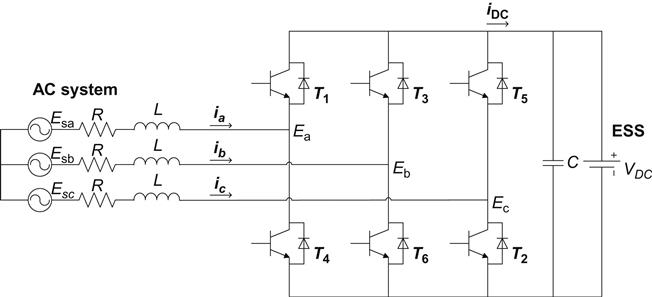
For many storage systems or DGs, the grid-tied inverter is the last converter to interface with the grid. It converts the DC power from DC ESS or DC link to AC power to supply the microgrid. Also, it absorbs AC power from the microgrid to charge the ESS. Most grid-tied inverters are VSI. The structure of a VSI is shown in Figure 3.33.
The basic control purpose is to control the real power and reactive power output, through decoupled PQ control. The direct-quadrature (dq) decoupling control is to control the power output of inverter by converting the abc three-phase power into dq-axes so that the real power and reactive power can be regulated independently.
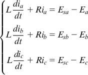
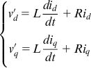
According to Figure 3.33, the relationship between the current and voltage of each phase is shown by Eq. (3.19).
(3.19)
 (3.19)
By performing the dq reference frame transformation, the current-voltage equation in dq-axes is obtained as in Eq. (3.20).
(3.20)
 (3.20)
where id and Vd denote the output current and voltage on d-axis. iq and Vq represent the values on q-axis. Now, assuming that
(3.21)
 (3.21)
Then, since ![]() and
and ![]() contains the first-order derivative of id and iq, Eq. (3.20) becomes
contains the first-order derivative of id and iq, Eq. (3.20) becomes
(3.22)
![]() and
and ![]() can be obtained by PI controller as in
can be obtained by PI controller as in
(3.23)
where ![]() . So the decoupled output current id and iq of the inverter can be controlled by performing the control strategy given by Eq. (3.22). The calculation results Vd and Vq can be transformed back to abc-axis to control the inverter. In addition, by employing another PI controller, output current references idref and iqref are generated from the real power and reactive power output errors. Therefore, the structure of the PQ controller for the grid-tied inverter can be designed as in Figure 3.34.
. So the decoupled output current id and iq of the inverter can be controlled by performing the control strategy given by Eq. (3.22). The calculation results Vd and Vq can be transformed back to abc-axis to control the inverter. In addition, by employing another PI controller, output current references idref and iqref are generated from the real power and reactive power output errors. Therefore, the structure of the PQ controller for the grid-tied inverter can be designed as in Figure 3.34.

As shown in Figure 3.34, a second PI controller is used to output the decoupled voltage signal in d-axis and q-axis respectively. The results are compensated by ωLiq and ωLid, respectively. After that, the control signal is transformed into abc-axis and then converted into a PWM signal to control the inverter.
3.7 Case Studies
3.7.1 The Control of Bidirectional Buck-Boost Converter
In recent years, with the development of battery technology, the performance of battery has increased dramatically while at the same time the price has gone down. So BESSs are used more often in the new microgrid projects. In this section, a case study of bidirectional buck-boost converter is presented as a simulation model in Simulink.
As Figure 3.35 shows, the converter has two IGBTs to deal with the buck mode and boost mode, respectively. The IGBTs are controlled by a controller. The controller of the converter has five inputs, which are “mode, Iref, Vref, Ifb, and Vfd.” The “mode” determines the operation mode of converter. If the input of “mode” is 1, the converter works in buck mode and the BESS is being charged, while the converter is in boost mode to discharge the BESS if “mode” is 0. Iref and Vref are the reference of charging current and the reference of discharging voltage. Ifb and Vfd are the inductor current and the converter voltage feedbacks. The output of a converter connects to a DC voltage source and a resistor, which represents a DC link in a microgrid.

The structure of the controller is shown in Figure 3.36. It consists of two proportional-integral-derivative (PID) controllers, one for the buck converter and the other for the boost converter. Each controller has a saturation to limit the output of PID to within −0.95 and 0.95 so that the control signal can be a valid duty cycle signal for the IGBTs. The PWM generators convert the duty cycle signal into a PWM signal to operate the IGBTs. When the “mode” signal is 1, the IGBT2, which connects to the G2 port in Figure 3.35, is linked to the buck controller. And the IGBT1 (G1 port) is always in the off-state due to the constant input 0. So the system becomes a buck converter and the DC voltage source can charge the BESS with the desired current value. If the “mode” signal is set to 0, the controller switches to boost mode, in which the IGBT1 is controlled by the boost controller and the input of IGBT2 is set to constant 0. In this mode, the converter can output energy from BESS to the DC link with desired voltage value. The simulation results of these two control modes are shown in Figures 3.37 and 3.38.

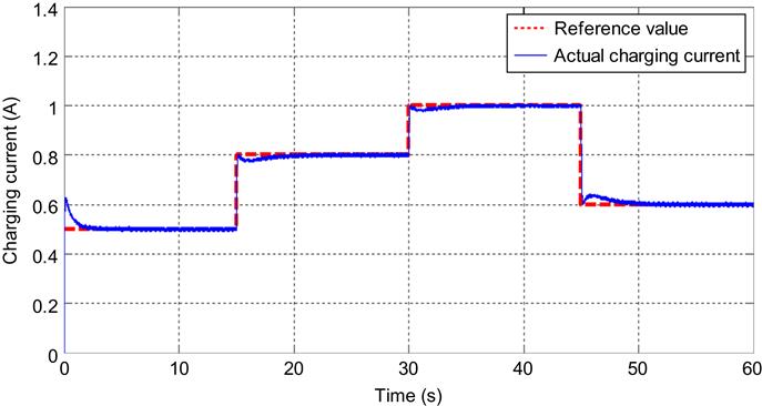

In Figure 3.37, the charging current control result is shown for 60 s. At first, the charging current reference is set to 0.5 A. At 15 s, the charging current reference is changed to 0.8 A and again to 1 A at 30 s. Finally, the charging current reference is stepped down to 0.6 A at 45 s. This simulation result indicates that the buck converter can control the charging current as the desired value. In a similar fashion, the result in Figure 3.38 shows that the voltage can follow the reference value well during ESS charging mode.
3.7.2 dq Control of VSI
In order to verify the validity of dq decoupling control in a grid-tied inverter system, a modeling and simulation case has been established in a Matlab/Simulink platform. The modeled grid-tied inverter system is presented in Figure 3.39.
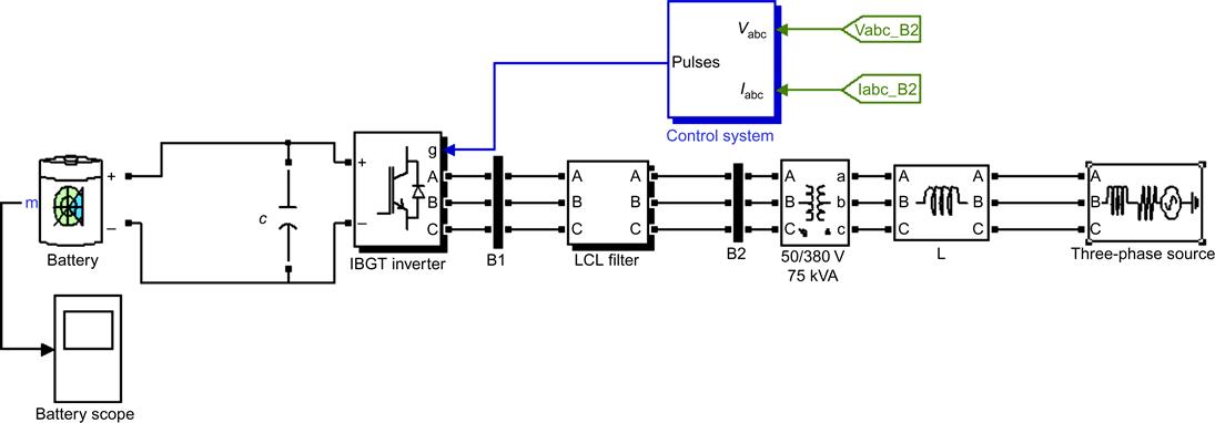
As shown in Figure 3.39, the DC voltage source, which can be viewed as the DG in microgrid, is a battery. In this case, the battery will either provide power for the microgrid during discharging mode or extract power from microgrid during charging mode. Its working mode depends on reference signal of the system. Along with the battery, a bidirectional VSC (IGBT converter) can either convert DC power into AC power like a conventional inverter or regulate AC power into DC power as a rectifier. An inductor-capacitor-inductor (LCL) filter is necessary for removing high order harmonics to avoid power quality problems in the microgrid. For the ESS system in Figure 3.39, the output voltage of battery is low and thus AC voltage output is not high enough for the microgrid. Therefore a transformer is used to change the voltage level. B1 and B2 are measurement tools which can detect three-phase voltage and current information. The control system is responsible for the control of the VSC. Some parameters of the VSC system have been listed in Tables 3.1 and 3.2. A detailed control system diagram is given in Figure 3.40.
Table 3.1
| Battery Type | Nominal Voltage | Rated Capacity | Initial SOC |
| Nickel-metal-hybrid | 100 V | 6.5 Ah | 50% |

Table 3.2
| Inductors of LCL Filter | Capacitor of LCL Filter | Voltage Amplitude of Three-Phase Voltage Source | Voltage Source Resistance | Voltage Source Inductance |
| 500 μH100 μH | 20 μF | 311 V | 0.1 Ω | 0.1e−3H |


Note that in the PQ control block, if the real power reference is positive, the ESS provides real power for microgrid through the VSC; and if the reactive power reference is positive, the ESS provides reactive power for microgrid through the VSC. However, if the real power reference or reactive power reference is negative, the power flow direction will be opposite.
The feedback signals are three-phase voltage and three-phase current from LCL output. The measured three-phase voltage is abbreviated as Vabc and three-phase current as Iabc. Then Vabc and Iabc are converted into the dq-axis for decoupling control. Vabc is converted into Vd and Vq while Iabc is converted into Id and Iq. Whereas, a phase-lock-loop (PLL) is included in order to synchronize the output of VSC with the grid system. Real power and reactive power are calculated in PQ computation block based on values of Vd, Vq, Id and Iq. Real power and reactive power are fed into PQ control block, as shown in Figure 3.41.
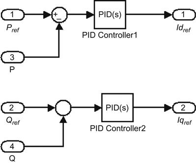
In order to control real power and reactive power independently, a dual-loop control strategy is employed in this case. From Figure 3.41, Id reference signal and Iq reference signal for current regulation are generated from the PQ control block. These two reference signals, Idref and Iqref, are fed into current regulator, as illustrated in Figure 3.42.

The establishment of current control structure follows Eqs. (3.20)– (3.23) in Section 3.6.2. Gain1 and Gain2 represent the coefficient ωL. The output signals Vdref and Vqref of the current regulators are used to generate PWM driving signals.
First, the real power reference value is set at 2400 W and the reactive power reference value at −1000 var. VSC system simulation results are given in Figures 3.43–3.46. It is worth mentioning that the simulation time range of all figures (except Figure 3.44) is 0.5 s.

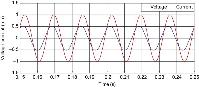


Figure 3.43 presents the real power and reactive power simulation results of grid-ties inverter system. The thicker solid line represents real power curve and the thinner solid line represents the reactive power curve. Also dotted line indicates real power reference and dashed line indicates reactive power reference. In this example, step signals are introduced into both the real power reference and the reactive power reference. Specifically, first the real power reference value is changed from 2400 to −1000 W and reactive power reference is changed from −1000 to 1000 var at 0.3 s. From Figure 3.43 it can be seen that the rise time of grid-tied inverter control system is less than 0.2 s and real power and reactive power are precisely controlled to the reference values. The simulation results are divided into two different sections which are battery charging section and battery discharging section. In conclusion, established VSC system is either able to charge the battery or provide power for microgrid.
Figure 3.44 shows the VSC output voltage and current waveform in phase A. It can be seen that voltage and current waveform are not in phase since reactive power output is not zero during 0.15–0.3 s.
Figure 3.45 presents battery SOC status of VSC system. Since simulation time is short, SOC does not change much from its initial value of 50%. Figure 3.45 presents the SOC curve during the discharging and charging process. This zoomed figure shows that power is indeed provided from battery to microgrid at discharging working mode and power is extracted from microgrid to battery at charging working mode.
Figure 3.46 shows battery voltage and current status of VSC system during discharging and charging working mode. From Figure 3.46 it can be seen that battery current was changed from positive to negative because battery working status is switched from discharging to charging.