“In real open source, you have the right to control your own destiny.”
—Linus Torvalds
When purchasing a computing device, users are concerned with the hardware configuration of the device and whether it has the latest versions of the software and applications. Most computer and consumer electronics device users don’t realize that there are several layers of programs that run between the user pressing the power button of the device and when the operating system starts running. These programs are called firmware.

A block diagram labeled system on chip S o C has nineteen components, B M C firmware, discrete graphics card, display panel, camera, battery, N V M E device, T C P C P D, T B T firmware, and others.
Typical computing system firmware inventory
Recent research from the LinuxBoot project on the server platform claims that the underlying firmware is at least 2.5x times bigger than the kernel. Additionally, these firmware components are capable. For example, they support the entire network stack including the physical layer, data link layer, networking layer, and transportation layer; hence, firmware is complex as well. The situation becomes worse when the majority of the firmware is proprietary and remains unaudited. Along with end users, tech companies and cloud service providers (CSPs) may be at risk because firmware that is compromised is capable of doing a lot of harm that potentially remains unnoticed by users due to its privileged operational level. For example, exploits in Base Management Controller (BMC) firmware may create a backdoor entry into the server, so even if a server is reprovisioned, the attacker could still have access into the server. Besides these security concerns, there are substantial concerns regarding performance and flexibility with closed source firmware.
This chapter will provide an overview of the future of the firmware industry, which is committed to overcoming such limitations by migrating to open source firmware. Open source firmware can bring trust to computing by ensuring more visibility into the source code that is running at the Ring 0 privilege level while the system is booting. The firmware discussed in this chapter is not a complete list of possible firmware available on a computing systems, rather just a spotlight on future firmware so you understand how different types of firmware could shape the future. Future firmware will make device owners aware of what is running on their hardware, provide more flexibility, and make users feel more in control of the system than ever.
Migrating to Open Source Firmware

A stacked concentric circle has eight layers labeled platform hardware, manageability firmware, system management mode, system firmware, kernel, device drivers, device drivers, and applications.
System protection rings
Let’s take a look into these “minus” rings in more detail.
Ring -1: System Firmware
System firmware is a piece of code that resides inside the system boot device, i.e., SPI Flash in most of the embedded systems, and is fetched by the host CPU upon release from reset. Depending on the underlying SoC architecture, there might be higher-privileged firmware that initiates the CPU reset (refer to the book System Firmware: An Essential Guide to Open Source and Embedded Solutions for more details).
Operations performed by system firmware are typically known as booting, a process that involves initializing the CPU and the chipsets part of systems on chip (SoCs), enabling the physical memory (dynamic RAM, or DRAM) interface, and preparing the block devices or network devices to finally boot to an operating system. During this booting process, the firmware drivers can have access to direct hardware registers, memory, and I/O resources without any restrictions. Typically, services managed by system firmware are of two types: boot services, used for firmware drivers’ internal communication and vanished upon system firmware being booted to the OS; and runtime services, which provide access to system firmware resources to communicate with the underlying hardware. System firmware runtime services are still available after control has transferred to the OS, although there are ways to track this kind of call coming from the OS layer to the lower-level firmware layer at runtime.
System firmware belonging to the SPI Flash updatable region qualifies for in-field firmware update, and also supports firmware rollback protection to overcome vulnerabilities.
Ring -2: System Management Mode
Hardware-based method: This triggers a system management interrupt (SMI), a dedicated port 0xb2 with the unique SMI vector number.
Software-based method: This uses a general-purpose interrupt through the Advanced Programmable Interrupt Controller (APIC).
During initialization of the system firmware, a code block (program) can get registered with an SMI vector, which will get executed while entering into SMM. All other processors on the system are suspended, and the processor states are saved. The program that is getting executed when in SMM has access to the entire system, i.e., processor, memory, and all peripherals. Upon exiting from SMM, the processor state is restored and resumes its operations as if no interruption had occurred. Other higher-level software doesn’t have visibility about this mode of operation.
SMM exploits are common attacks on computer systems, where hackers use SMI to elevate the privilege level, access the SPI control registers to disable the SPI write protection, and finally write BIOS rootkits into the SPI Flash.
The major concern with SMM is that it’s completely undetectable, so one doesn’t know what kind of operation is running in SMM.
Ring -3: Manageability Firmware
Ring -3 firmware consists of the separate microcontrollers running its firmware and later booted to a real-time operating system (RTOS). This firmware always remains on and is capable of accessing all the hardware resources; it’s meant to perform the manageability operations without which one might need to access these devices physically. For example, it allows the remote administration of the enterprise laptops and servers by IT admins, such as powering on or off the device, reprovisioning the hardware by installing the operating system, taking the serial log to analyze the failure, emulating the special keys to trigger recovery, performing active thermal management like controlling the system fans, and handling the critical hardware device failure like a bad charger, failure of storage device, etc.
Although this firmware has access to system resources (access to the host CPU, unlimited access to the host system memory and peripherals) of the host CPU (based on how it is being interfaced with the host CPU), the operations performed by these processors are “invisible” to the host processor. The code that is running on these processors is not publicly available. Moreover, these codes are provided and maintained by the silicon vendors; hence, they are assumed to be trusted without verifying through any additional security layer like a verified boot or secure boot.
The fact to consider here is that all these software codes are developed by humans and reviewed by other sets of humans. It’s possible to have some bugs exist irrespective of which layer of ring it’s getting executed in, and the concern is that the more privileged layer that gets executed, the more opportunity there is for hackers to exploit the system.
As per the National Vulnerability Database (NVD), there are several vulnerabilities being reported or detected by security researchers on production systems every year. Among those security defects there are many that exist within the “minus” rings. For example, CVE-2017-3197, CLVA-2016-12-001, CLVA-2016-12-002, CVE-2017-3192, CVE-2015-3192, CVE-2012-4251, etc., are vulnerabilities reported in firmware from the NVD.
Most of the firmware being discussed was developed using closed source, which means the documentation and code source to understand what’s really running on a machine is not publicly available. When a firmware update is available, you may be worried about clicking the accept button because you don’t have any clue whether this update is supposed to run on your machine. The user has a right to know what’s really running on their device. The problem with the current firmware development model is not the security; a study done on 17 open source and closed source software showed that the number of vulnerabilities existing in a piece of software is not affected by the source availability model that it uses. The problem is lack of transparency.
Transparency is what is missing in closed source firmware if we park the argument about the code quality due to internal versus external code review. All these arguments will point back to the need to have visibility into what is really running on the device that is being used. Having the source code available to the public might help to get rid of the problem of running several “minus” rings.
Running the most vulnerable code as part of the highest privileged level makes the entire system vulnerable; by contrast, running that code as part of a lesser privileged level helps to meet the platform initialization requirement as well as mitigates the security concern. It might also help to reduce the attack surface.
Additionally, performance and flexibility are other concerns that can be improved with transparency. For example, typically closed source firmware development focuses on short-term problems such as fixing the bugs with code development without being bothered about redundancy if any. A case study presented at the Open Source Firmware Conference 2019 claimed that a system is still functional and meets the booting criteria even after 214 out of 424 firmware drivers and associated libraries were removed, which is about a 50 percent reduction. Having more maintainers of the code helps to create a better code sharing model that overcomes such redundancy and results in instant boot. Finally, coming to the security concerns, having a transparent system is more secure than a supposed secure system that hides those potential bugs in closed firmware.
Firmware is the most critical piece of code running on the bare hardware with a privileged level that might allure attackers.
A compromised firmware is not only dangerous for the present hardware but all systems that are attached to it, even over a network.
Lower-level firmware operations are not visible to upper-level system software; hence, attacks remain unnoticed even if the operating system and drivers are freshly installed.
Modern firmware and its development models are less transparent, which leads to multiple “minus” rings.
Having a transparency firmware development model helps to restore trust in firmware as device owners are aware of what is running on the hardware. In addition, better design helps to reduce the “minus” rings, represents less vulnerability, and provides better maintenance with improved code size and higher performance.
Open source firmware (OSF) is the solution to overcome all of these problems. The OSF project performs a bare-minimum platform initialization and provides flexibility to choose the correct OS loader based on the targeted operating system. Hence, it brings efficiency, flexibility, and improved performance. Allowing more eyes to review the code while firmware is getting developed using an open source model provides a better chance to identify the feature detects, find security flaws, and improve the system security state by accommodating the community feedback. For example, all cryptographic algorithms are available in GitHub publicly. Finally, to accommodate the code quality question, a study conducted by Coverity Inc. finds open source code to be of better quality. All these rationales are adequate to conclude why migrating to OSF is inevitable. Future firmware creators are definitely looking into an opportunity to collaborate more using open source firmware development models.
This chapter will emphasize the future firmware development models of different firmware types such as system firmware, device firmware, and manageability firmware using open source firmware.
Open Source System Firmware Development
Most modern system firmware is built with proprietary firmware where the producer of the source code has restricted the code access; hence, it allows private modification only, internal code reviews, and the generation of new firmware images for updates. This process might not work with a future firmware development strategy where proprietary firmware is unreliable, or the functionality is limited in cases where device manufacturers relied on a group of firmware engineers who know only what is running on the device and therefore are capable of implementing only the required features. Due to the heavy maintenance demands of closed source firmware, often device manufacturers defer regular firmware updates even for critical fixes. Typically, OEMs are committed to providing system firmware updates two times during the entire life of the product, once at the launch and another six months later in response to an operating system update. System firmware development with an open source model in the future would provide more flexibility to users to ensure that the device always has the latest configuration. For that to happen, future system firmware must adhere to the open source firmware development principle. The open source firmware model is built upon the principle of having universal access to source code with an open source or free license that encourages the community to collaborate in the project development process.
This book provides the system architecture of several open source system firmware types including the bootloader and payload. Most open source bootloaders have strict resistance about using any closed source firmware binary such as binary large objects (BLOBs) along with open source firmware. Typically, any undocumented blobs are dangerous for system integration as they could be rootkits and might leave the system in a compromised state. But, the industry recognizes that in order to work on the latest processors and chipsets from the silicon vendors, the crucial piece of the information is the silicon initialization sequence. In the majority of cases, this is considered as restricted information prior to product launch due to innovation and business reasons and may be available under only certain legal agreements (like NDAs). Hence, to unblock the open source product development using latest SoCs, silicon vendors have come up with a proposal for a binary distribution. Under this binary distribution model, the essential silicon initialization code is available as a binary, which eventually unblocks platform initialization using open source bootloaders and at the same time abstracts the complexities of the SoC programming and exposes a limited set of interfaces to allow the initialization of SoC components. This model is referred to in this book as the hybrid work model.
Hybrid system firmware model: The system firmware running on the host CPU might have at least one closed source binary as a blob integrated as part of the final ROM. Examples: coreboot, SBL on x86 platforms.
Open source system firmware model: The system firmware code is free from running any closed source code and has all the native firmware drivers for silicon initialization. Example: coreboot on RISC-V platforms.
Hybrid System Firmware Model
Bootloader: A boot firmware is responsible for generic platform initialization such as bus enumeration, device discoveries, and creating tables for industry-standard specifications like ACPI, SMBIOS, etc., and performing calls into silicon-provided APIs to allow silicon initialization.
Silicon reference code binary: One or multiple binaries are responsible for performing the silicon initialization based on their execution order. On x86-platforms, Firmware Support Package (FSP) is the specification being used to let silicon initialization code perform the chipset and processor initialization. It allows dividing the monolithic blob into multiple sub-blocks so that it can get loaded into system memory as per the associated bootloader phase and provides multiple APIs to let the bootloader configure the input parameters. Typically, this mode of FSP operation is known as API mode. Unlike other blobs, the FSP has provided the documentation, which includes the specification and expectation from each API and platform integration guide. This documentation clearly calls out the expectations from the underlying bootloader, such as the bootloader stack requirement, heap size, meaning for each input parameter to configure FSP, etc.
Intel FSP Specification v2.1 introduces an optional FSP boot mode named Dispatch mode to increase the FSP adaptation toward PI spec bootloaders.
Payload: An OS loader or payload firmware can be integrated as part of the bootloader or can be chosen separately, which provides the additional OS boot logic.
coreboot using FSP for booting the IA-Chrome platform
EDKII Minimum Platform Firmware for Intel Platforms
coreboot Using Firmware Support Package
Firmware Support Package (FSP) provides key programming information for initializing the latest chipsets and processor and can be easily integrated with any standard bootloader. In essence, coreboot consumes FSP as a binary package that provides easy enabling of the latest chipsets, reduces time-to-market (TTM), and is economical to build as well.
FSP Integration
Configuration: The FSP provides configuration parameters that can be customized based on target hardware and/or operating system requirements by the bootloader. These are inputs for FSP to execute silicon initialization.
eXecute-in-place and relocation: The FSP is not position independent code (PIC), and each FSP component has to be rebased if it needs to support the relocation, which is different from the preferred base address specified during the FSP build. The bootloader has support for both these modes where components need to be executed at the address where it’s built, called eXecute-In-Place (XIP) components and marked as --xip, for example, FSP-M binary. Also, position-independent modules are modules that can be located anywhere in physical memory after relocation.
Interfacing: The bootloader needs to add code to set up the execution environment for the FSP, which includes calling the FSP with correct sets of parameters as inputs and parsing the FSP output to retrieve the necessary information returned by the FSP and consumed by the bootloader code.
FSP Interfacing

A framework of Firmware Support Package has six steps labeled, coreboot, F S P, F S P 1.0, F S P 1.1, F S P 2.0, and F S P 2.2 with four levels.
Explaining FSP interfacing with coreboot boot-firmware
coreboot supports FSP Specification version 2.x (the latest as of this writing is 2.2).
FSP Configuration Data

A tree structure has s r c on top, followed by vendor code, intel, f s p, f s p 2 underscore 0, tiger lake, and four different F S P U P D structures that has region signature, T component, M component, and S component, respectively.
UPD data structure as part of coreboot source code
It is recommended that the bootloader copy the whole UPD structure from the FSP component to memory, update the parameters, and initialize the UPD pointer to the address of the updated UPD structure. The FSP API will then use this updated data structure instead of the default configuration region as part of the FSP binary blob while initializing the platform. In addition to the generic or architecture-specific data structure, each UPD data structure contains platform-specific parameters.

A flow chart depicts the initialization of the F S P configuration data to the open source firmware development project.
coreboot code structure to override UPD data structures
OSF development efforts expect the entire project source code is available for review and configuration, but due to business reasons like innovation and/or competition, the early open sourcing of the FSP configuration data structure is not feasible for non-production-release qualification (PRQ) products. It poses risk while developing an open source project using the latest SoC prior to PRQ. Consequences of this restriction would be incomplete SoC and mainboard source code per platform initialization requirements and incomplete feature enabling.
This structure consists only of platform UPDs required for a specific bootloader to override for the current project.
The rest of the UPDs are renamed as reserved. For any project, reserved fields are not meant for bootloader overrides.
Embargoed UPD parameters’ names and descriptions are being abstracted.
First argument: This is the path for the complete FSP-generated UPD data structure. The tool will run on this header itself to filter out only the required UPD parameters as per the second argument.
Second argument: This is a file that provides the lists of required UPD parameters for bootloader overrides.
This effort will ensure complete source code development on the bootloader side along with enabling new features without being bothered about the state of the silicon release. Post SoC PRQ, after the embargo is revoked, the complete FSP UPD data structure gets uploaded into FSP on GitHub, which replaces all reserved fields of the partial header with the proper naming.
coreboot and FSP Communications Using APIs

A flow diagram has two layers, bootloader and F S P A P Is. Layer 1 has boot block, rom stage, post car, and ram stage. Layer 2 has F S P-T, F S P-M, and F S P-S. Both layers connect by arrows, along with a series of intermediate steps. A reset option connects to the bootblack step of layer 1.
coreboot boot flow using FSP in API mode
- 1.
coreboot owns the reset vector.
- 2.
coreboot contains the real mode reset vector handler code.
- 3.
Optionally, coreboot can call the FSP-T API (TempRamInit()) for temporary memory setup using (CAR) and create a stack.
- 4.
coreboot fills in the UPD parameters required for the FSP-M API, such as FspMemoryInit(), which is responsible for memory and early chipset initialization.
- 5.
On exit of the FSP-M API, either coreboot tears down CAR using the TempRamExit() API, if the bootloader initialized the temporary memory in step 3 using the FSP-T API, or coreboot uses the native implementation in coreboot.
- 6.
It fills up the UPD parameters required for silicon programming as part of the FSP-S API, FspSiliconInit. The bootloader finds FSP-S and calls into the API. Afterward, FSP returns from the FspSiliconInit() API.
- 7.
If supported by the FSP, the bootloader enables multiphase silicon initialization by setting FSPS_ARCH_UPD.EnableMultiPhaseSiliconInit to a nonzero value.
- 8.
On exit of FSP-S, coreboot performs PCI enumeration and resource allocation.
- 9.
The bootloader calls the FspMultiPhaseSiInit() API with the EnumMultiPhaseGetNumberOfPhases parameter to discover the number of silicon initialization phases supported by the bootloader.
- 10.
The bootloader must call the FspMultiPhaseSiInit() API with the EnumMultiPhaseExecutePhase parameter n times, where n is the number of phases returned previously. The bootloader may perform board-specific code in between each phase as needed.
- 11.
The number of phases, what is done during each phase, and anything the bootloader may need to do in between phases, will be described in the integration guide.
- 12.
coreboot continues the remaining device initialization. coreboot calls NotifyPhase() at the proper stage like AfterPciEnumeration, ReadyToBoot, and EndOfFirmware before handing control over to the payload.
If FSP returns the reset required status from any API, then the bootloader performs the reset as specified by the FSP return status return type.
Find the FSP header to locate the dedicated entry point, and verify the UPD region prior to calling.
Copy the default value from the UPD area into the memory to allow the required override of UPD parameters based on the target platform using driver-provided callbacks into the SoC code, for example: before calling into memory init or before silicon init.
Fill out any FSP architecture-specific UPDs that are generic like NvsBufferPtr for MRC cache verification.
Finally, call the FSP-API entry point with an updated UPD structure to silicon initialization.
On failure, handle any errors returned by FSP-API and take action; for example, manage the platform reset request to either generic libraries or SoC-specific code.
On success, retrieve the FSP outputs in the form of hand-off blocks that provide platform initialization information. For example, FSP would like to notify the bootloader about a portion of system memory that is being reserved by FSP for its internal use, and coreboot will parse the resource descriptor HOBs produced by the FSP-M to create a system memory map. The bootloader FSP driver must have capabilities to consume the information passed through the HOB produced by the FSP.
Current coreboot code has drivers for the FSP 1.1 and FSP 2.0 specifications. The FSP 2.0 specification is not backward compatible but updated to support the latest specification as FSP 2.2.
Bringing-up process: This enables application processors (APs) from a reset. It loads the latest microcode on all cores and syncs the latest Memory Type Range Register (MTRR) snapshot between BSP and APs.
Perform CPU feature programming: Allow vendor-specific feature programming to run such as to ensure higher power and performance efficiency, enable overclocking, and support specific technologies like Trusted eXecution Technology (TXT), Software Guard Extensions, Processor Trace, etc.
Typically, the bringing-up process for APs is part of the open source documentation and generic in nature. But, the previously listed CPU feature programming lists are expected to grow in the future and be considered proprietary implementations. If the system firmware implementation with the open source bootloader isn’t able to perform these recommended CPU features, programming might resist the latest hardware features. To overcome this limitation, the hybrid system firmware model needs to have an alternative proposal as part of the FSP driver.
Currently, coreboot is doing CPU multiprocessor initialization for the IA platform before calling FSP-S using its native driver implementation and having all possible information about the processor in terms of maximum number of cores, APIC IDs, stack size, etc. The solution offered here is a possible extension of coreboot support by implementing additional sets of APIs, which are used by FSP to perform CPU feature programming.
FSP uses the Pre-EFI Initialization (PEI) environment defined in the PI Specification and therefore relies on install/locate PPI (PEIM to PEIM Interface) to perform certain API calls. The purpose of creating a PPI service inside the bootloader is to allow accessing its resources while FSP is in operation. This feature is added into the FSP specification 2.1 onward where FSP is allowed to make use of external PPIs, published by boot firmware and able to execute by FSP, being the context master.
APIs as per the Specification | coreboot Implementation of APIs | APIs Description |
|---|---|---|
PeiGetNumberOfProcessor | get_cpu_count() to get processor count | Get the number of CPUs. |
PeiGetProcessorInfo | Fill ProcessorInfoBuffer: - Processor ID: apicid - Location: get_cpu_topology_from_apicid() | Get information on a specific CPU. |
PeiStartupAllAps | Calling the mp_run_on_all_aps() function | Activate all the application processors. |
PeiStartupThisAps | mp_run_on_aps() based on the argument logical_cpu_number | Activate a specific application processor. |
PeiSwitchBSP | Currently not being implemented in coreboot due to scoping limitations | Switch the bootstrap processor. |
PeiEnableDisableAP | Enable or disable an application processor. | |
PeiWhoAmI | Calling to activate the cpu_index() function | Identify the currently executing processor. |
PeiStartupAllCpus Only available in EDKII_PEI_MP_SERVICES2_PPI | mp_run_on_aps() based on MP_RUN_ON_ALL_CPUS | Run the function on all CPU cores (BSP + APs). |
- 1.
coreboot selects either CONFIG_MP_SERVICES_PPI_V1 or CONFIG_MP_SERVICES_PPI_V2 from the SoC directory as per the FSP recommendation to implement the MP Services PPI for FSP usage. coreboot does the multiprocessor initialization as part of ramstage early, before calling the FSP-S API. All possible APs are out of reset and ready to execute the restricted CPU feature programming.
- 2.
coreboot creates the MP (MultiProcessor) Services APIs as per PI Specification Vol 1, section 2.3.9, and is assigned into the EFI_MP_SERVICES or EDKII_PEI_MP_SERVICES2_PPI structure as per the MP specification revision.
- 3.
FSP-S to install EFI_MP_SERVICES or EDKII_PEI_MP_SERVICES2_PPI based on the structure provided by coreboot as part of the CpuMpPpi UPD. At the later stage of FSP-S execution, locate the MP Services PPI and run the CPU feature programming on APs.
- 4.
While FSP-S is executing multiprocessor initialization using Open Source EDKII UefiPkg, it invokes a coreboot-provided MP Services API and runs the “restricted” feature programming on APs.

A flow diagram has coreboot and F S P blocks. Each block has different stages. Coreboot has boot block, rom stage, ram stage, and A Ps. F S P has F S P-Notify, F S P-S, F S P-M, and F S P-T. Triangular labels, 1 to 4, are placed near various stages of the diagram.
coreboot-FSP multiprocessor init flow
This design would allow running SoC vendor-recommended restricted CPU feature programming using the FSP module without any limitation while working on the latest SoC platform (even on non-PRQ SoC) in the hybrid system firmware model. The CPU feature programming inside FSP will be more transparent than before as it’s using coreboot interfaces to execute those programming features. coreboot will have more control over running those programming features as the API optimization is handled by coreboot.
Today on the CrOS platform, the cbmem -c command is capable only of redirecting the coreboot serial log into the cbmem buffer using the bootloader driver. With this approach, the coreboot serial library may be used by FSP to populate serial debug logs.
The same can be used for post code-based debug methods as well.
Rather than implementing a dedicated timer library inside FSP, this method can be used by FSP to inject any programmable delay using the bootloader-implemented PPI, which natively uses the bootloader timer driver.
To summarize, a hybrid system firmware model in the future provides the ease of porting to a new silicon. It allows for bootloaders (coreboot, SBL, UEFI MinPlatform, etc.) to have an FSP interfacing infrastructure for finding and loading FSP binaries, configuring FSP UPDs as per platform need, and finally calling FSP APIs.
EDKII Minimum Platform Firmware
Since the introduction of the Unified Extensible Firmware Interface (UEFI) firmware in 2004, all Intel architecture platforms have migrated from legacy BIOS to UEFI firmware implementations. With a blistering speed, UEFI firmware has taken over the entire PC ecosystem to become the de-facto standard for system firmware. Historically, platforms that use UEFI firmware have been nourished and maintained by a closed group; hence, the source used in a platform that uses UEFI firmware remains closed source although the specifications are open standards. Details about the UEFI architecture and specification are part of System Firmware: An Essential Guide to Open Source and Embedded Solutions.
Over the years the platform enabling activity has evolved and demands more openness due to firmware security requirements, cloud workloads, business decisions for implementing solutions using more open standards, etc.
Minimum Platform Architecture

A block diagram has Min Platform Architecture with three layers at the top. Layer 1 has F S P, Min Platform and Core. Layer 2 has Silicon, Platform and Core AP Is, below layer 1. Layer 3 has a Board package. This flows to Server, Client, and I o T via 3 arrows. A legend below indicates the various types of components present.
MPA diagram
The MPA firmware stack demonstrates the hybrid-firmware development work model where it combines the several closed and open source components for platform initialization.
Core
Tianocore is an open source representation of the UEFI. EDKII is the modern implementation of UEFI and Platform Initialization (PI) specifications. Typically, the EDKII source code consists of standard drivers based on the various industry specifications such as PCI, USB, TCG, etc.
Silicon
A closed source binary model was developed and released by silicon vendors (example: Intel, AMD, Qualcomm etc.) with an intention to abstract the silicon initialization from the bootloader.
Prior to the MPA architecture, the FSP API boot mode was the de facto standard for silicon initialization when the bootloader needs to implement a 32-bit entry point for calling into the APIs as per the specification. This limits the adaptation of SoC vendor-released silicon binaries aka FSP toward a bootloader that adheres to the UEFI PI firmware specification. Traditionally, the UEFI specification deals with firmware modules responsible for platform initialization and dispatched by the dispatcher (Pre-EFI Initialization aka PEI and Driver eXecution Environment aka DXE core). To solve this adaptation problem in the UEFI firmware platform enabling model, a new FSP boot mode has been designed with the FSP External Architecture Specification v2.1 known as dispatch mode.
Dispatch Mode
The UEFI PI bootloader adhering to the MPA is equipped with a PCD database to pass the configuration information between bootloaders to FSP. This includes hardware interface configuration (typically, configured using UPD in API mode) and boot stage selection. Refer to the “Min-Tree” section to understand the working principle and MPA stage approach for incremental platform development.
PEI Core as part of Silicon Reference code blob aka FSP is used to execute the modules residing into the firmware volumes (FVs) directly.
The PEIMs belonging to these FVs are communicating with each other using PPI as per the PI specification.
The hand-off-blocks are being used to pass the information gathered in the silicon initialization phase with the UEFI PI bootloader.
The UEFI bootloader doesn’t use NotifyPhase APIs; instead, FSP-S contains a DXE driver that implements an equivalent implementation using a DXE native driver that is getting invoked at NotifyPhase() events.

Two blocks, U E F I P I Boot loader and F S P Binary. The former has a P C D database, and the latter has a P E I Core. Both connect by 2 flow arrows, namely, feature configuration using P C Ds and dispatch firmware volumes. There is a notify phase implementation option in D X E in block 2. Block 2 connects to block 1 at the bottom by a flow arrow.
FSP work model in dispatch mode with UEFI bootloader
UEFI Bootloader and FSP Communications Using Dispatch Mode
The communication interface designed between the UEFI bootloader and FSP in dispatch mode is intended to remain as close as possible to the standard UEFI boot flow. Unlike API mode, where the communication between the bootloader and FSP takes place by passing configuration parameters known as UPD to the FSP entry points, in dispatch mode the Firmware File Systems (FFSs) that belong to FVs consist of Pre-EFI Initialization Modules (PEIMs) and get executed directly in the context of the PEI environment provided by the bootloader. This can also be referred to as the firmware volume drop-in model. In dispatch mode, the PPI database and HOB lists prepared by FSP are shared between the bootloader and FSP.
- 1.
The bootloader owns the reset vector and SecMain as part of the bootloader getting executed upon the platform start executing from the reset vector.
- 2.
SecMain is responsible for setting up the initial code environment for the bootloader to continue execution. Unlike the coreboot workflow with FSP in API mode, where coreboot does the temporary memory initialization using its native implementation on the x86 platform instead calling the FSP-T API, dispatch mode tries to maximize the usage of FSP and uses FSP-T for initializing temporary memory and setting up the stack.
- 3.
The bootloader provides the boot firmware volume (BFV) to the FSP. The PEI core belonging to FSP uses the BFV to dispatch the PEIMs and initialize the PCD database.
- 4.
In addition to the bootloader PEI modules, FSP dispatches the PEI module part of FSP-M to complete the main memory initialization.
- 5.
The PEI core continues to execute the post-memory PEIMs provided by the bootloader. During the course of dispatch, the PEIM included within FSP-S FV is executed to complete the silicon-recommended chipset programming.
- 6.
At the end of the PEI phase, all silicon-recommended chipset programming is done using the closed source FSP, and DXE begins its execution.
- 7.
The DXE drivers belonging to the FSP-S firmware volume are dispatched. These drivers will register events to be notified at different points in the boot flow. For example, NotifyPhase will perform the callbacks to complete the remaining silicon-recommended security configurations such as disabling certain hardware interfaces, locking the chipset register, and dropping the platform privilege level prior to handing control off to the payload or operating system.
- 8.
The payload phase executes the OS bootloader and loads the OS kernel into the memory.
- 9.
The OS loader signals the events to execute the callbacks, registered as part of the DXE drivers to ensure the pre-boot environment has secured the platform.
Platform
Generic: This part remains generic in nature by providing the required APIs to define the control flow. This generic control flow is being implemented inside MinPlatformPkg ( Edk2-Platforms/Platform/Intel/MinPlatformPkg), such that the tasks performed by the MinPlatformPkg can be reused by all other platforms (belonging to the board package) without any additional source modification.
Board package: This part focuses on the actual hardware initialization source code aka board package. Typically, the contents of this package are limited to the scope of the platform requirements and the feature sets that board users would like to implement. As described in Figure 1-8, the board package code is also open source and represented as Edk2-Platforms/Platform/Intel/<xyz>OpenBoardPkg, where xyz represents the actual board package name. For example, TiogaPass, a board supported by Open Compute Project (OCP) based on Intel’s Purley chipset, uses the PurleyOpenBoardPkg board package.
A closed source representation of the OpenBoardPkg is just BoardPkg, which still directly uses the MinPlatformPkg from EDKII platforms.
A board package may consist of one or more supported boards. These boards are sharing the common resources from the board package.
Board-specific source code must belong to the board directory and name after the supported board. For the previous example, the board directory for TiogaPass is named as BoardTiogaPass.
All the board-relevant information is made available to the MinPlatformPkg using board-defined APIs.
To summarize MPA, it consists of a closed source FSP package for silicon initialization, and the rest of the source code is potentially open source where MinPlatformPkg and a board package are combined together to call the platform.
Min-Tree
MPA is built around the principle of a structural development model. This structural development model can be referred to as a min-tree, where the source code tree is started with a minimalistic approach and enriched based on the required functionality getting included over time as the platform is getting matured. To make this model structural, the design principle relied on dividing the flow, interfaces, communication, etc., into a stage-based architecture (refer to “Minimum Platform Stage Approach” section).

A graph of min-tree over product timeline. There are three layers. From bottom to top, there is a minimum platform, advanced features, and product differentiator. The components reduce per layer from bottom to top. There are two stages, from left to right, namely Early and later development cycles. The first block in layer 1 has two units.
Min-tree evolution over product timeline
The later product development stages are targeted more toward meeting the product milestone releases; hence, it focuses on the code completion that includes development of the full feature sets applicable for this platform. Next is platform development, which focuses on the enablement of the product differentiator features, which is important for product scaling. Finally, the platform needs to be committed to sustenance, maintenance, and derivative activities. The staged platform approach is a more granular representation form of the min-tree where based on product requirement, timeline, security, feature sets, etc., one can decide the level of the tree to design the minimum platform architecture. For example, product-distinguishing features are not part of the essential or minimum platform or advanced feature list, and the board package is free to exclude such features using boot stage PCD (gMinPlatformPkgTokenSpaceGuid.PcdBootStage). This may be used to meet a particular use case based on the platform requirement. For example, a board may disable all advanced features by setting the board stage PCD value to 4 instead of 6 to improve the boot time. Decrementing the additional stages might also be used for SPINOR size reduction as the final bootloader executable binary size is expected to get reduced.
Minimum Platform Stage Approach
The MPA staged approach describes the minimal code block and binary components required while creating system firmware. The flexible architecture allows modifying the FD image to make it applicable for the target platform. In this architecture, each stage will have its own requirement and functionality based on the specific uses. For example, Stage III, Boot to UI, is focused on interfacing with console I/Os and other various hardware controllers using the command-line interface. Additionally, decrementing a stage might also translate to reducing the platform feature set. For example, a Stage III bootloader won’t need to publish ACPI tables as this feature is not useful for the platform.
Figure 1-11 describes the stage architecture, including the expectations from the stage itself. Each stage is built upon the prior stage with extensibility to meet the silicon, platform, or board requirements.
Stage I: Minimal Debug

A flow chart has two platforms, minimum and full, with 7 stages. The minimum platform has 1 to 6 stages. The full platform has a whole 7 stages. The stages are, Minimal debugging, memory functional, boot to U I, boot to OS, security enabled, advanced feature selection, and optimization.
Minimum platform stage architecture
Stage I is contained within the SEC and PEI phases; hence, it should get packed and uncompressed inside the firmware volume. The minimal expectation from this stage is to implement board-specific routines that enable the platform debug capability like serial output and/or postcode to see the sign of life.
This is similar to all other bootloaders that come up on a memory-restricted environment like x86. Perform initialization of temporary memory and set up the code environment.
Perform pre-memory board specific initialization (if any).
Detect the platform by reading the board ID after performing the board-specific implementation.
Perform early GPIO configuration for the serial port and other hardware controllers that are supposed to be used early in the boot flow.
Enable the early debug interface, typically, serial port initialization over legacy I/O or modern PCH-based UARTs.
The functional exit criteria of Stage I is when temporary memory is available and the debug interface is initialized where the platform has written a message to indicate that Stage I is now getting terminated.
Stage II: Memory Functional
Stage II (Memory Functional) is primarily responsible for ensuring the code path that executes the memory initialization code for enabling the platform permanent memory. This stage extends the operations on top of Stage I and performs the additional/mandatory silicon initializations required prior to memory initialization. Because of the memory-restricted nature of platform boot, this stage is also packed uncompressed. Stage II is more relying on the FSP-M firmware volume in terms of finding the PEI core and dispatching the PEIMs.
Perform pre-memory recommended silicon policy initialization.
Execute memory initialization module and ensure the basic memory test.
Switch the program stack from temporary memory to permanent memory.
The functional exit criteria of Stage II are that early hardware devices like GPIOs are being programmed, main memory is initiated, temporary memory is disabled, memory type range registers (MTRRs) are programmed with main memory ranges, and the resource description HOB is built to pass that initialization information to the bootloader.
Stage III: Boot to UI
The primary objective of Stage III (Boot to UI) is to be able to successfully boot to the UEFI Shell with a basic UI enabled. The success criteria of this stage is not to demonstrate that every minimum platform architecture should be equipped with the UEFI Shell, but rather more focuses on the generic DXE driver execution on top of the underlying stages like Stages I and II (mainly targeted for silicon and board). The bare-minimal UI capability required for Stage III is a serial console.
Bring generic UEFI-specific interfaces like DXE Initial Program Load (IPL), DXE Core, and dispatch DXE modules. This includes installing the DXE architectural protocols.
Perform post-memory silicon-recommended initialization.
Have a provision to access the nonvolatile media such as SPINOR using UEFI variables. Additionally, capabilities that can be enabled as part (but not only limited to this lists) of this phase allow various input and output device driver access such as USB, graphics, storage, etc.
The functional exit criteria of Stage III is to ensure all generic device drivers are not operational and the platform has reached the BDS phase, meaning the bootloader is able to implement minimal boot expectations for the platform.
Stage IV: Boot to OS
Leveraging on the previous stage, Stage IV (Boot to OS) is to enable a minimal boot path to successfully boot to an operating system (OS). The minimal boot path is the delta requirement over Stage III that ensures booting to an OS.
Add minimum ACPI tables required for booting an ACPI-compliant operating system. Examples are ACPI tables, namely, RSDT (XSDT), FACP, FACS, MADT, DSDT, HPET, etc.
Based on the operating system expectation, it might additionally publish DeviceTree to allow the operating system to be loaded.
Trigger the boot event that further executes the callbacks being registered by the FSP-S PEIMs to ensure locking down the chipset configuration register and dropping the platform privilege prior to launching the application outside trusted boundaries.
This phase will also utilize the runtime services being implemented by the UEFI bootloader for communication like Timer and nonvolatile region access from the OS layer.
After the platform is able to successfully boot to a UEFI-compliant OS with a minimal ACPI table being published, it is enough to qualify Stage IV to call its termination. Additionally, this stage implements SMM support for x86–based platforms where runtime communication can get established based on software triggering SMI.
Stage V: Security Enable
The basic objective of Stage V (Security Enable) is to include security modules/foundations incrementally over Stage IV. Adhering to the basic/essential security features is the minimal requirement for the modern computing systems. Chapter 5 is intended to highlight the scenarios to understand the security threat models and what it means for the platform to ensure security all around even in the firmware.
Ensure that the lower-level chipset-specific security recommendation such as lockdown configuration is implemented.
Hardware-based root of trust is being initialized and used to ensure that each boot phase is authenticated and verified prior to loading into the memory and executing it as a chain throughout the boot process.
Protect the platform from various memory-related attacks if they implement the security advisory well.
At the end of this phase, it will allow running any trusted and authenticated application including the operating system.
Stage VI: Advanced Feature Selection
Advanced features are the nonessential block in this min-tree structural development approach. All the essential and mandatory features required for a platform to reach an operating system are developed using stages I to V. The advanced feature selection is focused on developing firmware modules based on a few key principles such as modularization, reducing interdependencies over other features, etc. It helps these modules to get integrated with min-tree as per the user requirements, product use cases, and even the later product development cycle.
Platform development models become incremental where more essential features are integrated and developed at an early phase. Otherwise, the complex but generic advanced features can be developed without being bottlenecked on the current silicon and board but can be readily shared across platforms.
Advanced feature modules necessarily do not contain functionality that is unrelated to the targeted feature.
Each feature module should be self-content in nature, meaning it minimizes the dependencies to the other feature.
The feature should expose a well-defined software interface that allows easy integration and configuration. For example, all modules should adhere to EDKII configuration options such as PCD to configure the feature.
Stage VII: Optimization
In the scope of current architecture, Stage VII (Optimization) is a proposed architectural stage reserved for future improvements. The objective of this stage is to provide an option for the platform to ensure optimization that focuses on the target platform. For example, on a scaling design without Thunderbolt ports, there should be a provision using PCD that disables dispatching of Thunderbolt drivers (including host, bus, and device). This is known as a configurable setting.
Additionally, there could be compilation-time configuration attached to the PCD that strips unused components from the defined FV. For example, FSP modules are used for API boot mode. It is intended that such optimization/tuning can be intercepted in the product even at a later stage without impacting the product milestone aka schedules.
These are just examples that demonstrate the architecture freedom to improve the platform boot time and SPINOR size reduction at the later stage.
To summarize, a hybrid system firmware development using EDKII MPA is intended to improve the relationship between open source and closed source components. An MPA design brings transparency to platform development even with EDKII platform code. The min-tree design serves as a basic enablement vehicle for the hardware power-on and allows cross-functional teams to get started on feature enablement. The feature enablement benefits from its modular design that is simple to maintain.
Open Source System Firmware Model
The ideal philosophy of open source system firmware is to make sure that all pieces of the firmware are open source, specifically, the ones required for the boot process post CPU reset. This effort of achieving the system firmware code is 100 percent open source and has significant dependency over the underlying platform hardware design. Typically, due to the unavailability of the detailed hardware interface document and programming sequence for boot-critical IPs like memory controller, system firmware projects should choose the hybrid system firmware model over complete open source system firmware. RISC-V is a good example of an open standard hardware specification that allows pure open source system firmware development on RISC-V-based embedded systems, personal computers, etc. The word pure being used here intentionally to differentiate a firmware project that supports closed source blobs for platform pre-reset flow from the transparent system reset flow (pre and post CPU reset) with all possible open source firmware.
There are several open source system firmware projects available, and this section is about having a detailed overview about expectations from the future open source system firmware. Hence, future system firmware will focus not only on getting rid of proprietary firmware blobs but also on adopting a modern programming language for developing system firmware. oreboot is an aspiring open source system firmware project that is slowly gaining momentum by migrating its supports from evaluation boards to real hardware platforms. oreboot has a vision of pure open systems, meaning firmware without binary blobs. But to add the latest x86-based platforms, it had made an exception to include only boot-critical blobs (for example, manageability firmware, AMD AGESA, FSP for performing specific silicon initialization), where feature implemented by blobs during boot is not possible to implement in oreboot.
This section will provide an architecture overview of oreboot and its internals, which will be valuable for developers to learn for preparing themselves for system firmware architecture migration into a more efficient and safe programming language. It’s like a recurrence of events that happened a few decades back that had migrated the present system firmware programming language to C from assembly.
oreboot = Coreboot - C + Much More
oreboot is focused on reducing the firmware boundary to ensure instant system boot. The goal for oreboot is to have fewer than one boot on embedded devices.
It improves the system firmware security, which typically remains unnoticed by the platform security standards with a modern, safe programming language. Refer to Appendix A for details about the usefulness of Rust in system firmware programming, which deals with direct memory access and even operations that run on multithreaded environments.
It removes dedicated ramstage usage from the boot flow and defines a stage named Payloader Stage. This will help to remove the redundant firmware drivers and utilities from LinuxBoot as payload.
It jumps to the kernel as quickly as possible during boot. Firmware shouldn’t contain the high-level device drivers such as network stack, disk drivers, etc., and it can leverage the most from LinuxBoot.
Currently, oreboot has support for all the latest CPU architecture, and adding support for the newer SoC and mainboards are a work in progress. Currently the RISC-V porting being done using oreboot is fully open sourced. In addition, it’s able to boot an ASpeed AST2500 ARM-based server management processor as well as a RISC-V OpenTitan “earlgrey” embedded hardware.
oreboot Code Structure
Directory | Description |
|---|---|
src/arch | Lists of supported CPU architecture, for example: armv7, armv2, risc-v, x86, etc. |
src/drivers | Supported firmware drivers, written in Rust, that follow oreboot unique driver model, for example: clock, uart, spi, timer, etc. |
src/lib | Generic libraries like devicetree, util, etc. |
src/mainboard | Lists of supported mainboards as part of the oreboot project. This list contains emulation environments like qemu, engineering board such as upsquared based on x86, and HiFive the RISC-V based development board, BMC platform ast2500, etc. Each mainboard directory contains a makefile and Cargo.toml file to define the build dependencies, which will allow it to build all boards in parallel. Example of Cargo.toml: [dependencies] cpu = { path = "../../../cpu/armltd/cortex-a9"} arch = { path = "../../../arch/arm/armv7"} payloads = { path = "../../../../payloads"} device_tree = { path = "../../../lib/device_tree" } soc = { path = "../../../soc/aspeed/ast2500" } [dependencies.uart] path = "../../../drivers/uart" features = ["ns16550"] Include source files written in Rust (.rs) and assembly (.S) as per the boot phase requirements. Two special files reside in the mainboard directory as fixed-dtfs.dts to create the flash layout and describe system hardware configuration as mainboard.dts. mainboard.dtb is the binary encoding of the device tree structure. |
src/soc | Source code for SoC that includes clock programming, early processor initialization, setting up code environment, DRAM initialization sequence, chipset registers programming, etc. Each SoC directory also contains Cargo.toml that defines the dependent drivers and library required for SoC-related operations. |
payloads/ | Library for payload-related operations like loading into memory and executing. |
tools/ | Tools directory that contains useful utilities like layoutflash to create an image from binary blobs, as described in the layout specified using device tree, bin2vmem to convert binary to Verilog VMEM format, etc. |
README.md | Describes the prerequisites to getting started with oreboot, cloning source code, compilation, etc., useful for the first-time developer. |
Makefile.inc | This makefile is included by the project mainboard directory makefile. |
oreboot Internals
This section will guide developers through the various key concepts of oreboot that are required to understand its architecture. Without understanding these architectural details, it would be difficult to contribute to a project. Also, these are the key differentiating features for oreboot, compared to the coreboot project.
Flash Layout
Flash layout specifies how different binaries as part of oreboot are getting stitched together to create the final firmware image (ROM) for flashing into the SPI Flash. This file is named fixed-dtfs.dts, belonging to each mainboard directory.
oreboot has replaced the coreboot file system (CBFS) with the Device Tree File System (DTFS). It is easy to expose the layout of the flash chip without any extra OS interface. DTFS provides an easy method to describe the different binary blobs.

A layout of the six components is depicted in an interface, Boot Blob, fixed D T F S, N V R A M, empty space, rom payload, and ram payload.
32MiB flash layout
The description field defines the type of binary, offset is the base address of the region, the size field specifies the region limit, and the file field is used to mention the path of the binary. x is the region number inside the flash layout, for example: boot blob, rampayload, NVRAM, etc. With reduced boot phases, the oreboot architecture allows ample headroom in flash.
Build Infrastructure

A flowchart for ore boot build has four levels in the middle of four layers. They are cargo build, rust object copy, layout flash, and device tree compiler. There are three input flows for each layer, namely, the Arch directory, the Mainboard directory, and the Payload directory. The flow diagram ends with the Final Binary ore boot dot bin.
oreboot build flow
Create an executable and linking format (ELF) binary from source code using the cargo build command.
Convert the .elf file to binary format (.bin) with the rust objcopy command.
The output binary (.bin) belongs to a region specified using the file field as part of the flash layout file. Now these binaries need to construct an image that will be flashed into the device. The tool name layoutflash is (source code belongs to the tools directory as mentioned earlier) used to construct the final binary (.ROM). It takes arguments as an oreboot device tree to specify the image layout and compiled binary files generated by the compilation process.
Device Tree
The DTS specification specifies a construct called a device tree, which is typically used to describe system hardware. A device tree is a tree data structure with nodes that describe the device present in the system. Each node has a value that describes the characteristics of the device. At compilation, the boot firmware prepares the device information in the form of device tree that can’t necessarily be dynamically detected during boot, and then during boot, the firmware loads the device tree into the system memory and passes a pointer to the device for the OS to understand the system hardware layout. Unlike coreboot, the device tree structure prepared by oreboot is more scalable and can be parsed by existing OSs without any modification.
Hardware device tree: Part of the mainboard directory, this is used to describe the system hardware that the system firmware is currently running. This is typically named after the mainboard; for example, a device tree name for RISC-V processor–based development board HiFive is hifive.dts.
oreboot device tree: This is the device tree used to define the layout of the image that is flashed into the device.

A flow chart illustrates the main board of oreboot hi Five. It starts with the root node, then flows to four nodes, namely, c pus, memory, r e f c l k, and serial, from top to bottom. c pus flows to c p u at the rate of zero and one, respectively.
Device tree example from oreboot HiFive mainboard
In the previous example, cpus, memory, refclk, and serial are node names, and root node is identified by a forward slash (/). @ is used to specify the unit-address to the bus type on which the node sits.
Driver Model
Driver Functions | Description |
|---|---|
init() | Initializes the device. |
pread() | Positional read. It takes two arguments: - First argument: A mutable buffer that will get filled data from the driver. - Second argument: The position that one would like to read from. The function returns the result; the type of the result could be either a number, defined the number of bytes being read, or an error. If there are no more bytes to read, it returns an end-of-file (EOF) error. |
pwrite() | Positional writing. It takes two arguments: - First argument: A buffer that contains data is used by the driver to write on the hardware. - Second argument: The position that one would like to write into. The function returns the number of bytes written. |
shutdown() | Shuts down the device. |
Physical device drivers: The drivers that are used to operate on real hardware devices like memory drivers are capable of performing reads/writes to physical memory addresses, serial drivers used to read/writes to serial devices, clock drivers to initialize the clock controller present on the hardware, and DDR drivers to perform DRAM-based device initialization.
Virtual drivers: Drivers that are not associated with any real hardware device but rather used to create the interface for accessing the hardware device. For example, the union driver is capable of stream input or output to multiple device drivers; refer to the following example of mainboard, which implements the union driver for a serial device; and section reader, which reads a section from another device window specified using offset and size and returns EOF when the end of the window is reached.
oreboot Boot Flow
The boot flow defined by oreboot is similar to coreboot, except for the fact that oreboot has accepted that a firmware boundary has to be reduced, so it makes sense to leverage more from the powerful payload offerings as LinuxBoot with a more mature Linux kernel driver. oreboot replaces the need to have a dedicated stage like ramstage, which is meant to perform an operation that can be replaced by a powerful payload and load a payload. The oreboot boot flow provides an option to load the Linux kernel as part of the flash image as the payload from the payloader stage.
Some of the work done in a coreboot project is separating the payload loading and running operations from a dedicated stage like ramstage and having a flexible design where the bootloader is free to decide which stage can be used to load the payload. This work is known as Rampayload or coreboot-Lite, which influences the design of oreboot having an independent stage for payload operations and being called from prior stages as per the platform requirements.
Bootblob: This is the first stage post CPU reset, which is executed from the boot device. It holds the first instruction being executed by the CPU. This stage is similar to coreboot’s first stage called bootblock.
Romstage: This is functionally similar to the coreboot romstage boot phase, which is intended to perform the main memory initialization.
Payloader stage: This is only intended to load and run the payload. This is a feature differentiator from the coreboot, where the ramstage boot state machine has tasks to load and run payload at the end of hardware initialization.

A schematic diagram of the Si Five-Hi Five processor. The components are S P I Flash, Serial Console, U 54-M C Core plex, P R C I, S P I controllers, U A R T controllers, D D R controller, and D RAM, all connected by flow arrows.
Hardware block diagram of SiFive-HiFive Unleashed
In this example, RISC-V SoC has four pins (0001, MSEL0 is 1 and MSEL1-3 are set to 0) called MSEL to choose where the bootloader is, and Zeroth Stage Boot Loader (ZBL) is stored in the ROM of the SoC. ZBL loads oreboot from the SPI Flash, and control reaches the bootblob.
Bootblob
The early piece of the code in bootblob is written in assembly, which is executed by the CPU immediately after release from power-on reset. It performs the processor-specific initialization as per the CPU architecture.
It sets up the temporary RAM as Cache as RAM, aka CAR or SRAM, as physical memory is not yet available.
It prepares the environment for running Rust code like setting up the stack and clearing memory for BSS.
It initializes UART(s) to show the sign-of life using the debug print message “Welcome to oreboot.”
It finds the romstage from the oreboot device tree and jumps into the romstage.
soc/sifive/fu540/src/bootblock.S | |
|---|---|
/* Early initialization code for RISC-V */ .globl _boot _boot: # The previous boot stage passes these variables: # a0: hartid # a1: ROM FDT # a0 is redundant with the mhartid register. a1 might not be valid on # some hardware configurations, but is always set in QEMU. csrr a0, mhartid setup_nonboot_hart_stack: # sp <- 0x02021000 + (0x1000 * mhartid) - 2 li sp, (0x02021000 - 2) slli t0, a0, 12 add sp, sp, t0 # 0xDEADBEEF is used to check stack underflow. li t0, 0xDEADBEEF sw t0, 0(sp) # Jump into Rust code call _start_nonboot_hart |

A block diagram of boot blob stage has the components S P I flash and Serial Console and connect to P R C I, S P I, and U A R T controllers. These connect to U 54-M C Core plex and D D R Controller, which finally connects to DRAM. The components are classified as inactive or disabled state, active or enabled state, and initialization in progress.
Operational diagram of bootblob stage
Romstage
Perform early device initialization, for example configuring memory-mapped control and status register for controlling component power states, resets, clock selection and low-level interrupts, etc.
Initiate the DRAM initialization. Configure memory controllers as part of the SoC hardware block. This process involves running SoC vendor-specific routines that train the physical memory or implementing memory reference code in Rust (basically a direct porting from C to Rust). For the HiFive Unleashed platform, oreboot has implemented DDR initialization code in Rust belonging to soc/sifive/fu540/src/ddr*.rs by referring to open source FSBL implementation.
A flow diagram of rom stage S P I flash connects to F U 540-C 0 0 0 and S P I controllers, and Serial console connects to U ART controllers. These two, along with P R C I, connect to the U 54-M C complex and the D D R controller. Then it connects to DRAM. The stages are inactive or disabled, active or enabled, and initialization in progress.
Operational diagram of romstage
Payloader Stage

A flow diagram has three labels, inactive or disabled, active or enabled, and initialization in progress. S P I flash and Serial console are connected to S P I and U ART controllers, which along with P R C I connect to U 54-M C core plex and D D R controller, which connects to DRAM. The payloader stage of D RAM connects to F U 540-C 0 0 0.
Operational diagram of payloader stage
Payload
An oreboot project by default uses LinuxBoot as a payload, which allows it to load the Linux kernel from the SPI Flash into DRAM. The Linux kernel is expected to initialize the remaining devices using kernel drivers that include block devices and/or network devices etc. Finally, locate and load the target operating system using kexec. LinuxBoot uses u-root as initramfs, which is the root filesystem that the system has access to upon booting to the Linux kernel. systemboot is an OS loader as part of u-root to perform an iterative operation to attempt boot from a network or local boot device.

A flow diagram has three labels, inactive or disabled, active or enabled, and initialization in progress. S P I flash and Serial console are connected to S P I and U ART controllers, which along with P R C I connect to U 54-M C core plex and D D R controller, which connects to DRAM. The Linux boot of D RAM connects to F U 540-C 0 0 0.
Operational diagram of payload stage

A flow diagram has three labels, inactive or disabled, active or enabled, and initialization in progress. S P I flash and Serial console are connected to S P I and U ART controllers, which along with P R C I connect to U 54-M C core plex and D D R controller, which connects to DRAM. The Kernel of D RAM connects to F U 540-C 0 0 0.
System hardware state at the kernel
To summarize, the complete open source system firmware model using oreboot like the bootloader is not only meant to provide freedom from running proprietary firmware blobs on hardware. Additionally, it’s developed using safe system programming languages like Rust. The payloader userland is written in Go and advocates the architectural migration of the system firmware development using a high-level language in the future. Finally, a reduced boot phase allows ample free space in the flash layout, which will provide an opportunity to reduce the hardware bill of materials (BoM) cost with instant boot experience.
Open Source Device Firmware Development
System firmware is the firmware that is running on the host CPU after it comes out from the reset. In traditional computing systems, system firmware is owned by independent BIOS vendors (IBVs), and adopting the open source firmware model will help to get visibility into their code. This will help to design a transparent system by knowing the program is running on the underlying hardware, and it provides more control over the system. Earlier sections highlighted the path forward for system firmware development in the future using open source system firmware as much as possible. In a computing system, there are multiple devices that are attached to the motherboard, and each device has its own firmware. When a device is powered on, firmware is the first piece of code that runs and provides the required instructions and guidance for the device to be ready for communicating with other devices or for performing a set of basic tasks as intended. These types of firmware are called device firmware. Without device firmware being operational, the device wouldn’t be able to function. Based on the type of the devices, a complexity in the firmware is introduced. For example, if a device is a simple keyboard device, then it has only a limited goal and no need to worry about regular updates, whereas more complex ones, like graphics cards, need to define an interface that allows it to interact with the system firmware and/or an operating system to achieve a common goal, which is to enable the display.
The majority of device firmware present on consumer products is running proprietary firmware that might lead to a security risk. For example, at the 2014 Black Hat conference, security researchers first exposed a vulnerability in USB firmware that leads to a BadUSB attack, a USB flash device, which is repurposed to spoof various other device types to take control of a computer, pull data, and spy on the user. A potential solution to this problem is that device firmware should be developed using open source so that the code can be reviewed and maintained by others rather than only the independent hardware vendors (IHVs).
This section will describe the evolution in device firmware development for discrete devices that has a firmware burned into its SPINOR.
Legacy Device Firmware/Option ROM

A graphic card is drawn. P C L-E x4/x8 is named at one of the parts of the given graphic card. The ports available are H D M I, D P, Serial Port, Debug port, which connects to Display, Audio, U ART, J TAG, and D D R connects to D D R x. Option ROM connects to S P I, which flows to P C I-E x 4 over x 8.
Discrete graphics card hardware block diagram
A common example of OpROM is the Video BIOS (VBIOS), which can be used to program either on-board graphics or discrete graphics cards and is specific to the device manufacturer. In this section, VBIOS is referred to and used to initialize the discrete graphics card after the device is powered on. It also implements an INT 10h interrupt (interrupt vector in an x86-based system) and VESA BIOS Extensions (VBE) (to define a standardized software interface to display and audio devices) for both the pre-boot application and system software to use.
Offset | Length | Value | Description |
|---|---|---|---|
0x00 | 0x02 | 0xAA55 | Signature |
0x02 | 0x01 | Varies | Option ROM length |
0x03 | 0x4 | Varies | Initialization vector |
0x07 | 0x13 | Varies | Reserved |
0x12h | 0x02 | Varies | Offset to PCI data structure |
0x1A | 0x02 | Varies | Offset to PnP expansion Header structure |
Signature: All ISA expansion ROMs are currently required to identify themselves with a signature word of AA55h at offset 0. This signature is used by the system firmware as well as other software to identify that an option ROM is present at a given address.
Length: The length of the option ROM in 512 byte increments.
Initialization vector: The system BIOS will execute a far call to this location to initialize the option ROM. The field is four bytes wide even though most implementations adhere to the custom of defining a simple three-byte NEAR JMP. The definition of the fourth byte may be OEM specific.
Reserved: This area is used by various vendors and contains OEM-specific data and copyright strings.
Offset to PCI data structure: This location contains a pointer to a PCI data structure, which holds the vendor-specific information.
Offset to PnP expansion header: This location contains a pointer to a linked list of option ROM expansion headers.
The system firmware performs a read operation to read the first two bytes of the PnP OpROM structure and verifies the signature as 0xAA55. If a valid option ROM header is present, then the system firmware reads the offset + 02h to get the length of the OpROM and then performs a far call to offset + 03h to initialize the device. After video OpROM has initialized the graphics controller, it provides lists of services like setting the video mode, character and string output, and other VBE functions to operate in graphics mode.
General Video Service Functions (AH = 00 to FF, except 0x4F) | ||
|---|---|---|
Operation | Function | Subfunction |
Set Video Mode | AH=0x00 | AL=Video Mode |
Set Cursor Characteristics | AH=0x01 | CH bits 0-4 = start line for cursor in character cell bits 5-6 = blink attribute (00=normal, 01=invisible, 10=slow, 11=fast) CL bits 0-4 = end line for cursor in character cell |
Set Cursor Position | AH=0x02 | DH,DL = row, column BH = page number (0 in graphics modes; 0–3 in modes 2 and 3; 0–7 in modes 0&1) |
Write String (AT, VGA) | AH=0x13 | AL = mode BL = attribute if AL bit 1 clear BH = display page number DH,DL = row,column of starting cursor position CX = length of string ES:BP -> start of string |
VBE Functions (AH = 0x4F and AL = 0x00 to 0x15) | ||
Return VBE Controller Information | AH=0x4F | AL = 0x00; ES:DI = Pointer to buffer in which to place VbeInfoBlock Structure. |
Return VBE Mode Information | AH=0x4F | AL = 0x01; CX = Mode Number; ES:DI = Pointer to ModeInfoBlock Structure. |
Set VBE Mode | AH=0x4F | AX = 02h BX = Desired Mode to set ES:DI = Pointer to CRTCInfoBlock structure |

A block diagram has P C I Enumeration with P C I Device limit, Load P C I Op ROM, initialize the card which branches into prepare real mode, call Op ROM entry point and set VESA mode, and display boot splash. Call Op ROM and Set VESA mode both branch into three and two layers.
Discrete graphics card hardware block diagram
In this sample implementation, the system firmware calls video OpROM to initialize the graphics controller and uses video services to set the display to show the pre-OS display screen or OS splash screen during boot.

An interface of the computer system displays video BIOS option ROM at address 0 x C 0 0 0 0. There are ten lines of output on the display screen.
Display video BIOS option ROM at address 0xC0000

An interface has the initialization vector address at address 0 x C 0 0 0 3. A series of output lines are displayed on the screen.
Initialization vector address at address 0xC0003
This execution of OpROM for device initialization has several limitations while working with modern firmware solutions. Option ROM attacks can be considered an initial infection or ones to spread malicious firmware from one firmware component to another. Compromised OpROM firmware can be viewed as an initial method of infection that remains persistent even after modifying the system firmware. There is still a legacy implementation, where the system firmware and/or payload relies on the option ROM for device initialization and runtime services. Therefore, modern devices like discrete graphics cards and network cards still need to support legacy OpROMs.
UEFI OpROM
It has a modern and well-defined interface, which is implemented using an industry-standard specification.
All GPUs within a platform become “equal,” and there’s no more unique “VGA-enabled VGA.”
Code is written in C and doesn’t need a legacy interrupt handler to communicate between the platform and GPU.
Implementing UEFI graphics OpROM using EBC (EFI Byte Code) allows a single image to operate on multiple CPU architectures.
There are clearer and portable solutions that allow new features to be implemented.
Supported(): The “Supported” method of the GOP driver binding protocol tests to see whether the given handle is a manageable adapter. Also, check that EFI_DEVICE_PATH_PROTOCOL and EFI_PCI_IO_PROTOCOL are present to ensure that the handle that is passed is a valid PCI device. The PCI I/O protocol gets the PCI configuration header from the device and verifies that the device is supported by the present GOP driver.
- Start(): The “Start” method of the GOP driver binding protocol tells the graphics driver to start managing the controller. The GOP driver uses the device-specific knowledge to perform the following operations:
Initialize the graphics adapter.
Initialize platform parameters like LID Present, Dock Supported, etc.
Initialize the display manager module that enumerates all the supported displays and checks its live status and EDID to detect the enabled display device.
Create child handles for each detected and enabled physical output device and install the EFI_DEVICE_PATH_PROTOCOL.
Get EDID information from each enabled physical output device and install EFI_EDID_DISCOVERED_PROTOCOL on the child handle.
Create child handlers for each valid combination of two or more video output devices and install EFI_DEVICE_PATH_PROTOCOL.
Set the initial mode, required to initialize the mode field of GOP.
Install the GRAPHICS_OUTPUT_PROTOCOL on the selected device.
Stop(): The Stop function performs the opposite operation of the Startfunction. In general, Stop() functions uninstall all protocols, close the protocol instances, release all resources, and disable the graphics adapter.

A Block diagram of the graphics output protocol has U E F I GOP driver, Graphics Child Handle, Graphics Output Protocol, P C I input-output protocol, other input-output abstraction layers, and Graphics adapter. Each layer is connected by arrows.
GOP driver implementation
The QueryMode() function is used to return extended information on one of the supported video modes. It’s important that QueryMode() only return modes that can actually be displayed on the attached display device.
The SetMode() function allows system firmware to select the specific mode based on the mode argument, between 0 and numModes.
The Blt() function is used for transferring information to and from the video buffer. It allows graphics contents to be moved from one location of the video frame buffer to another location of the video frame buffer.
The GRAPHICS_OUTPUT_PROTOCOL.Mode pointer is populated when the graphics controller is initialized and gets updated with the SetMode() function call. The FrameBufferBase member of this object may be used by a UEFI OS loader or OS kernel to update the contents of the graphical display after ExitBootServices() is called and the Graphics Output Protocol services are no longer available. A UEFI OS may choose to use this method until a graphics driver can be installed and started.

A diagram depicts two option ROM headers and two PCIR headers. Option ROM and PCIR header 1 has video B I O S S legacy OpROM image, uncompressed and unsigned. Header 2 has generic G O P U E F I display driver image and compress signed.
Hybrid ROM layout
Figure 1-26 shows the layout of the hybrid OpROM image located on a graphics add-on card.
Set a Display Mode | Retrieve EDID from a Display Device | Display Switch | |
|---|---|---|---|
GOP Driver | GRAPHICS_OUTPUT_PROTOCOL.SetMode() | Using EFI_EDID_DISCOVERED_PROTOCOL | Reentrant with different child handle in EFI_DRVER_BINDING.Start() followed by a SetMode() |
Legacy VGA BIOS | Set VBE Mode using AX = 0x4F02 and other subfunctions | VBE DDC Extension AX = 0x4F15 and other subfunctions | Implement vendor-specific VGA BIOS extension |
Currently, the majority of GPU vendors have migrated graphics device firmware to a GOP driver–based solution for add-on graphics cards or on-board GPU to be legacy-free. The GOP driver images that are part of the add-on graphics card can be signed and authenticated by the vendor and can be verified using Secure Boot. But for the hybrid image on an add-on graphics card, Secure Boot is unable to verify the legacy OpROM image as the legacy VGA BIOS doesn’t support authentication and hence is considered to be a security threat.
Why Is Open Source Device Firmware Needed?
Performance: As most device firmware is not able to handle the runtime updates and becomes stale over the period of time, it may not be able to work with the latest processor and chipsets. Open source firmware development would provide an opportunity to update the device firmware code with the latest algorithm and research that would provide better performance compared to proprietary firmware.
Security: Open source device firmware doesn’t allow any hidden backdoor for snooping into the system. As device firmware would get regular maintenance, common vulnerabilities are expected to get fixed and updated without any delay.
Extensibility: While vendor device firmware comes with fixed sets of capability, open source firmware would expose its capability beyond its fixed scope.
Community support: The open source community provides more eyes and hands for maintaining the code.
Cost: The product source code is available freely using a GPL license and hence doesn’t require any subscription and licensing fees.
Many wireless routers are using open source device firmware. For example, TP-Link, which is Xiaomi router firmware, is derived from OpenWrt, an open source firewall/router distribution based on the Linux kernel.
Open Source Manageability Firmware Development

A block diagram of the Remote system joined with the management server via in-band management. Remote system has management access, applications, operating system, system firmware, and hardware.
High-level diagram of in-band remote management

A block diagram of the Remote system joined with the management server via out-of-band management, written over a two-way arrow. Remote system has applications, operating systems, system firmware, and hardware, and a management controller. The last two levels are connected by two-way arrows.
High-level diagram of out-of-band remote management
The modern server motherboards are the default coming with a built-in remote management controller. The out-of-band remote management can use either dedicated network interface controllers (NICs) or shared NICs for remote access. The shared NIC can be used for multiplexing the Ethernet connection between the host system operating system and the remote management controller so that while incoming traffic flows on the hardware, it is routed to the remote management controller before reaching the host system. It also has multiple interfaces like Enhanced Serial Peripheral Interface (LPC/eSPI), PCIe, SMBUS, USB, etc., to communicate with the host system.
Keyboard-video-mouse (KVM): Out-of-band management allows access to host CPU resources like the keyboard, video, and mouse, which provides broadcasting of video output to the remote terminals, and receiving the input from the remote keyboard and mouse can be used to configure the system firmware settings even prior to booting the OS.
Perform remote recovery: An admin can also access remote system disk images from the local boot media or over a network and therefore can be used to recover the system in case the OS crashes and the system reaches an OS recovery.
Remote power on/off: The remote administrator can schedule wake and update-like features to ensure the system is always updated with critical security patches. It also ensures the system’s availability over the network 24/7 using resource preservation by keeping the device in low-power mode after an update.
Remote sessions: It allows client-initiated remote sessions to monitor, manage, and troubleshoot any pre-OS and OS-related defects.
Out-of-band management requires seamless access of the system, and the remote management controller belongs to the platform hardware. The firmware that is running as part of the remote management controller is considered to be highly privileged components (Ring -3 as described earlier). This firmware remains active during the entire life of the system and can even control the system when it is powered off. Thus, any vulnerability that exists in the manageability firmware can easily remain hidden from the traditional security measures and put the entire system at risk where intruders can take over the system remote management and allow data exfiltration attacks.
This section will provide a brief overview of some manageability firmware that was developed using proprietary firmware and looking at the possibilities of migrating to the open source firmware.
Baseboard Management Controller

A schematic diagram of the motherboard server has multiple components connected to each other by flow arrows.
Server motherboard hardware block diagram with BMC
Ethernet: The Reduced Media-Independent Interface (RMII) and Reduced Gigabit Media-Independent interface (RGMII) are interfaces to connect an Ethernet MAC block to a PHY chip.
Flash memory: This is the Serial Peripheral Interface (SPI) flash memory that contains the BMC firmware for booting the SoC.
Memory: This is 800Mbps DDR3 or 1600Mbps DDR4 memory with 16-bit data bus width. Having more memory provides increased performance.
PCIe: The on-chip PCIe 2D VGA provides a local display capability with resolution up to 1920×1200 without adding an extra VGA add-on card.
USB: The USB 2.0 virtual hub controller allows up to five devices and a USB 1.1 HID device controller for keyboard and mouse support.
LPC/eSPI: This is a Low Power Count (LPC) or Enhanced SPI (eSPI) bus for communicating with the host.

A block diagram has A S T 2500 S o C block with C P U and six divisions, three on each side. On the left are36 k S RAM, S P I, and U S B controllers. On the right are U ART and D D R 3 or 4 controllers and P H Y block. S P I flash connects to the S P I controller. The serial console, D RAM, and Ethernet are on the right side.
AST2500 hardware block diagram
BMC allows system administrators to make use of KVM functionality for remote redirection of the keyboard, video, and mouse to a remote network-attached management console. Hence, it allows the remote admin to perform the low-level tasks while the operating system is not yet available.
Intelligent Platform Management Interface
OS-independent scenarios: Regular monitoring of platform-critical components like temperature. Various built-in sensors in the computer system and power supply voltage allow remote access to the system if the host system is powered off. It allows changing the BIOS settings for recovery boot and/or installing new operating systems into the block device.
While the OS is running: It allows the admin to access the operating system login console remotely to manage services such as installing virtual drives, populating management data and structures to the system management software, etc.

A framework of the I P M I subsystem has two block diagrams. The top diagram has Intelligent Platform Management Controllers, along with Baseboard and Chassis management controllers. The below diagram has the system interface and its branch components. Both blocks are connected by a system bus, I P M I messages, and System-B M C interfaces.
IPMI subsystem block diagram
There is a significant concern that the BMC is a closed infrastructure that allows administrators to have direct access to the host systems. A direct serial connection to the BMC is not encrypted, and the connection over the LAN may or may not use encryption and might raise the platform security risks. The following sections provide some serious security concerns with BMC and the reason for open source adaptation in the BMC project.

A pictorial representation of remote server management. The remote console divides into three types of B M C chips, which connect to three different servers and then flow to the internet and the various clients.
Remote server management using BMC-IPMI
The assumption was that the admins would be managing the computer systems over the trusted and controlled network, and the IPMI stack doesn’t pay great attention to ensuring security. Many BMC firmware doesn’t implement Secure Boot. The BMC is the ultimate security liability due to its privileged operations, and a compromised BMC would allow attackers to have access to a remote network connection, which had been in the realm of physical administrative access.
The BMC would allow the remote admin to access the OS console and mount the virtual media, typically used for recovering remotely or installing a custom OS image. A group of security researchers has found a severe BMC vulnerability on a server platform where the virtual media service allows plaintext authentication, allows unencrypted data over network, uses a weak encryption algorithm using a fixed key compiled into the BMC firmware, and possibly allows authentication bypass while authenticated to the virtual media service. These weaknesses would allow an attacker to gain unauthorized access to the virtual media. The BMC hardware allows the creation of virtual USB devices. Hence, upon authenticating using a well-known default username and password for the BMC, an attacker would be able to perform any of a USB-based attacks against the server remotely including data exfiltration, booting from untrusted OS images, or direct manipulation of the system using a virtual keyboard and mouse. A study also reveals that more than 47,000 BMCs from different countries are exposed to the Internet. Also, an attacker who compromises the host system could use it to attempt to compromise the BMC as well, as BMC always remains on without power-off. Hence, it would be difficult to remove such malware from the BMC. A BMC rootkit could provide the attacker with backdoor access that remains hidden from IPMI access logs and insusceptible to host OS reinstallation or password changes. In 2019, a vulnerability was detected on the BMC chip, where malware could be installed on the BMC from the local host via the PCIe or LPC interface. Because of the closed nature of the IPMI implementation, once attackers gain control of the BMC, it’s difficult to know their presence and remove them from the system. Such requirements lead the data centers to adopt the BMC firmware that is getting developed using open source projects.
OpenBMC
The OpenBMC project is a Linux Foundation project, which is intended to replace the proprietary BMC firmware with a customizable, open source firmware implementation. OpenBMC is a Linux distribution for management controllers that is used in devices such as servers, rack switches, telecommunications, etc. In 2014, four Facebook engineers at Facebook’s hackathon event created the first prototype of the open source BMC firmware, called OpenBMC for BMC inside the Wedge (a rack switch developed by Facebook) platform. In 2018, OpenBMC became a Linux Foundation project. OpenBMC uses the Yocto Project for creating the building and distribution framework. It uses D-Bus as an interprocess communication (IPC) method. OpenBMC includes a web application for interacting with the firmware stack. OpenBMC added Redfish support for hardware management.
Redfish is an open industry-standard specification used for hardware management. It is defined by the Distributed Management Task Force (DMTF). OpenBMC uses Redfish as a replacement for IPMI over LAN.
Host management: power on/off, cooling, LEDs, inventory, and events
Compliant to the IPMI 2.0 specification
Code update support for multiple BMC/BIOS images
Provides web-based user interface
REST management: BMCWeb Redfish, host management using REST APIs
SSH-based SOL
Remote KVM
Virtual media, etc.
Both the bootloader and the Linux kernel include various SoC-specific firmware and hardware drivers like I2C, USB, PWM, and SPI drivers, etc.
The open source packages include common applications such as busybox, i2c tools, openssh, and Python.
The board-specific package includes initialization scripts and tools that are specific to a board. Examples are a tool that dumps inventory from the EEPROM and a fan-controller daemon to control the fan speed based on environment readings.

A block diagram divides into four blocks, application, kernel, firmware, and hardware, from top to bottom. Each block has components of the S o C, and Board layers.
OpenBMC Stack on the Wedge platform
Common Layer | This layer includes packages that can be used across different SoCs and boards. For example: common/recipes-rest common/recipes-connectivity common/recipes-utils |
SoC Layer | The SoC layer includes packages that are specific to BMC SoCs. Figure 1-29 shows the SoC layer is part of both the bootloader and Linux driver as it implements a specific driver to communicate with the Aspeed BMC chipset. For example: meta-aspeed/recipes-bsp/u-boot meta-aspeed/recipes-core meta-aspeed/recipes-kernel/linux |
Board Layer | The packages being included in this layer are specific for the current board. Figure 1-29 shows the configuration, initialization scripts, and tools that are specific for Wedge. For example: meta-aspeed/recipes-core meta-aspeed/recipes-kernel meta-aspeed/recipes-wedge |
Generating an OpenBMC image for a specific board requires these three layers: the common layer, a SoC layer for the BMC SoC used in the board, and a board-specific layer for the targeted BMC board.
u-bmc
u-bmc is a project that was developed almost at the same time as OpenBMC. u-bmc is a Linux OS distribution for the BMC that was developed using open source firmware. The goal of u-bmc is to ensure that critical and highly privileged code like the BMC is easy to audit and adheres to modern security. u-bmc was written in Go and replaces the industry-standard IPMI with gRPC to reduce the attack surface and provide improved security.

An interface displays u-b m c firmware boot flow in detailed view. Several lines of software code depict the DRAM, warning, flash, using default environment, In and out, error and net.
u-bmc firmware boot flow
u-root incorporates four different projects as follows:
Go versions for standard Linux tools, for example: ls, cp, etc.
To compile many Go programs into a single binary
To create a Go-based userland that works as initramfs for the Linux kernel
Go bootloaders that use kexec to boot Linux kernels
It’s possible to ship the entire server firmware development using open source firmware where the system firmware is developed using coreboot, and u-bmc can be used for the BMC to boot the Linux distribution.
RunBMC

A block diagram flows from the host system motherboard with 260 Pin S O D I M M transformed into 260 pin Gold digger in the B M C daughter card. The B M C daughter card has various components connected via signal interfaces.
RunBMC daughterboard card block diagram
This design is more stable and secure because it modularizes the BMC subsystem, where the entire security effort is now shifted onto a single BMC card. It provides an opportunity to vendors for hardening the hardware security independently by adding security features like Titan, Cerberus, or TPM chips into the daughter card to implement a hardware-based root of trust. Also, a swappable BMC card is easy to replace if detected vulnerable or updated, without impacting the entire host system.
To summarize, out-of-band management for computing systems is an innovation that saves costs and minimizes the computer downtime on failure without physically visiting the data centers. But the availability of monitoring, accessing, and controlling the host system using BMC might increase the platform attack surface due to the closed source nature of BMC firmware and the higher privileged level that it operates. In the past, the security researchers have done ample studies to highlight the BMC vulnerabilities. The OpenBMC project sets the stage for BMC firmware and hardware development using an open source model. Having an open source hardware interface and BMC firmware developed with open source firmware provides visibility into the utmost privileged rings of the platform security, which was always closed otherwise.
Zephyr OS: An Open Source Embedded Controller Firmware Development
This section provides a brief overview of the embedded controller (EC) that is often found in low-power embedded systems and is responsible for managing various tasks that the system firmware and an operating system can’t handle. It’s important to understand the EC hardware control block, its communication with the host system, etc. This knowledge is essential to establish the trust in the system boot process, as the firmware that is running as part of the EC is an independent entity in the computing system that is capable of accessing the platform components directly. The majority of EC projects are developed using proprietary code; hence, it’s important to have visibility into all firmware that is part of the computing system.
Embedded Controller
Battery charging: Tasks includes managing the battery charger and the battery, detecting the presence of AC, and reporting its change status.
Thermal management: Tasks include measuring the temperature of board components (CPU, GPU, several sensors on board) and taking action to control the fan speeds, CPU throttling, or force power off based on critical sensor data.
Keyboard: The EC is also referred to as the keyboard system controller (KSC), which takes care of receiving and processing signals from the keyboard.
Hardware buttons and switches: Tasks include receiving and processing signals from hardware buttons (typically laptop/tablet button array) and switches (laptop lid).
Backlight, LEDs: The EC implements the LED’s control indicators (RGB) for battery, power, AC, caps lock, num lock, scroll lock, sleep, etc. Also, it is able to control the display and keyboard backlight.
Peripheral control: The EC is able to turn on and off several platform components like WiFi, Bluetooth, USB, etc.
Debug interface: The EC controller provides a UART port for serial debug and a Port 80h BIOS debug port. These are primarily used for testing, debugging, and remote administration of the device.

An embedded controller flow diagram depicts that S R A M and R O M are described clearly in the computer interface. It branches into various operational components.
Generic embedded controller block diagram
There are two possible ways that define how the EC should access its user code from SPI Flash.
Master attached flash sharing (MAFS): In this mode, the EC won’t have a dedicated SPI Flash; rather, it shares the SPI Flash with the host system PCH. EC will access SPI Flash over the eSPI flash sharing channel.
Slave attached flash sharing (SAFS): The EC will have access to dedicated SPI Flash using the SPI interface, and PCH will access SPI Flash over the eSPI flash sharing channel.
After the user code starts executing, it configures the GPIOs as per the platform needs and initializes the host interface. The EC and host system can communicate with each other using EC HOST commands and trigger ACPI events for interrupting host system and memory-mapped regions shared between EC and Host CPU address space. The following is an embedded controller firmware architecture overview so you can understand the internals of EC operations that help to perform independent tasks in a timely manner.
EC Firmware Architecture
Embedded controller firmware is responsible for performing the platform power sequencing and remains active all the time even when the platform control reaches the operating system. It needs to perform several independent tasks such as thermal monitoring, battery management, keyboard control, etc. This section will provide a high-level firmware architecture overview so you can understand the innards operations being managed by the EC.
Tasks
Most of the operations being performed by the embedded controller are in the context of a task. Since embedded controllers are not multicore, the scheduling of the tasks is done using some time slicing algorithm to achieve the multitask execution. Each task has its own fixed stack size assigned. There is no heap (malloc) to use, and all variable storage is explicitly declared at build time. Each task has its given priority, and it continues to run until it exits or a higher-priority task wakes up and takes control away from a lower-priority task. At a high level, it’s a loop that initiates all tasks unless there are wait eventsor a define sleep duration before resuming a task.
Callbacks
Callbacks allow you to register a function to get executed at a later point of time when a particular event occurs such as a callback to handle all button change events. Typically, these callbacks are registered by one module and invoked by different modules. If more than one callback needs to be run at the same time, then it’s getting called as per the priority order.
GPIOs
The board-specific code inside the EC source is to configure the GPIOs to allow SoC power transition and system transitions. The GPIOs can be configured as inputs, outputs, and interrupts. Typically, these are getting configured as part of the board init() function or based on certain callbacks like power off() while the system is transiting its state. The interrupt handles part of each module to read the GPIO status prior to transferring the call into the handle functions.
Modules
Operations being managed by the embedded controller are grouped into modules, and each module is self-contained after the GPIOs are configured. This includes initialization sequence, state machines, and interrupt handlers. Examples of such modules are peripheral management, power sequencing, SMC host, battery management, thermal management, KBC host, etc.
Debugging
Serial console: This is the traditional approach while developing or debugging EC firmware, where a serial console would be handy to indicate the problem. Also, some EC implementations use the static console buffer for ease of debugging, while the host reset doesn’t clear this buffer and persists across multiple reboots. An interactive EC console would help to run various key commands and system management independent of the host system.
Exception handler: If the EC firmware runs into an error, the easiest way to inform the user about the problem is by dumping the current operating stack. The exception handler contains some interesting information like the program counter (pc) and link register (lr), which indicates the code that the EC was running when the panic occurred.
Port 80 display: Initialize the port 80 display and use this to indicate any error in the following format: ECxx, where xx refers to the specific error code.
Host CPU to EC Communication
Host commands
Embedded controller interface
Shared memory map
Host Commands
The host CPU communicates with the EC by issuing host commands. These commands are identified by a command ID. When a host CPU is intended to issue a command (and data) to the EC, depending on the current operation phase (i.e., system firmware/BIOS or OS), it involves other software components. If system firmware is sending the host commands, it can directly send them to the EC, but from the OS layer, it first communicates via the EC kernel drivers, and then it receives the raw commands and sends them on the EC. The host packet is received by the EC board-specific code, which further sends the command to the common layer that runs the host command. While this is happening, the EC needs to indicate to the host that it is busy processing and not yet ready to give a response. If the host command expects a response, then the EC responds with the result and data to the host CPU. An example of a host command is to read the board ID by sending the SMCHOST_GET_FAB_ID command 0x0D to the EC.
Embedded Controller Interface
- The embedded controller command set allows operating system–directed configuration and Power Management (OSPM) to communicate with the EC. The ACPI defines the commands between 0x80 and 0x84 to tell the EC to perform an operation. For example, the Read Embedded Controller (RD_EC) command 0x80 allows OSPM to read a byte in the address space of the embedded controller.
The host waits for the Input Buffer Full (IBF) flag on the EC_SC to be 0.
The host writes the command byte to port 0x66 and the address byte to port 0x62.
The EC generates SCIs in response to this transaction from the SMC ACPI handler.
The SMC command handler passes control to the actual EC SoC code. To receive data from the EC, wait for Output Buffer Full (OBF) to be set, which indicates there is incoming data.

A block diagram depicts the A C P I specifications used for implementing the interface with different host interfaces.
Embedded controller shared interface
- When the embedded control has detected a system event that must need to communicate to OSPM, it first sets the SCI_EVT flag in the EC_SC register, generates an SCI, and then waits for OSPM to send the Query Embedded Controller (QR_EC) command 0x84. The OSPM driver detects the EC SCI when the SCI_EVT (SCI event is pending) flag in the EC_SC register is set and sends the QR_EC command. Upon receipt of the QR_EC command byte, the embedded controller places a notification byte value between 0x00 and 0xFF, indicating the cause of the notification. OSPM driver query ACPI control method with that value in the form of _Qxx where xx is the number of the query acknowledged by the embedded controller. Here’s an example to explain the scenario better:
A change in the LID switch status would trigger an GPE from the GPE bit (LAN_WAKE_N) tied to an embedded controller.
The OSPM driver queries the EC to know the query number.
The host system firmware has implemented a control method (_Qxx) corresponding to the OSPM query.
The ACPI control method notifies OSPM that the LID switch status has changed to Notify (LID0, 0x80); LID0 is ACPI device entry for LID.
The OSPM driver further calls the LID ACPI device control method to read the LID switch status (LIDS).
LID switch status can be read using the EC ACPI command either through port 0x62/0x66 or through the LPC register.
Upon reading from the EC, the ACPI control method passes the value to the OSPM driver, and the OS takes the necessary action.

A block diagram flows from two lids labeled open and closed lids. Then it connects to the embedded controller, Host system, O S P M driver, and finally to System firmware A C P I and A S L.
Software implementation of the EC control interface
Shared Memory Map
Some systems have memory regions shared between the embedded controller and the host system address space. The size of this memory region is limited and treated as read-only (RO) on the host system side. This memory is maintained by the EC to pass various interesting information such as battery status, thermal sensor data, battery information, fan speed, LID switch status, etc. A system that doesn’t support this shared memory needs to send host commands to read that information.
Challenges with Closed Source EC Firmware
The firmware that is running as part of the embedded controller is working at a higher privileged level where unauthorized access won’t be detected by the security controller running as part of the system firmware or an OS. Also, if proprietary EC firmware code doesn’t implement Secure Boot or verified boot, then it’s allowed to run even unsigned and untrusted images. There have been several vulnerabilities being reported in the past where the EC can run unsigned firmware, and having a compromised EC firmware results in a denial-of-service (DoS) attack on the system. To bring more reliability and efficiency to computing systems and allow visibility into the most privileged code that is running prior to the host CPU reset, the industry is promoting an open source and collaborative embedded controller development using the Zephyr OS.
The next section will provide details about developing EC firmware using an open source advantage, but prior that, let’s understand the reference hardware design that enables independent EC development using a Modular Embedded Control Card (MECC).
Modular Embedded Controller Card
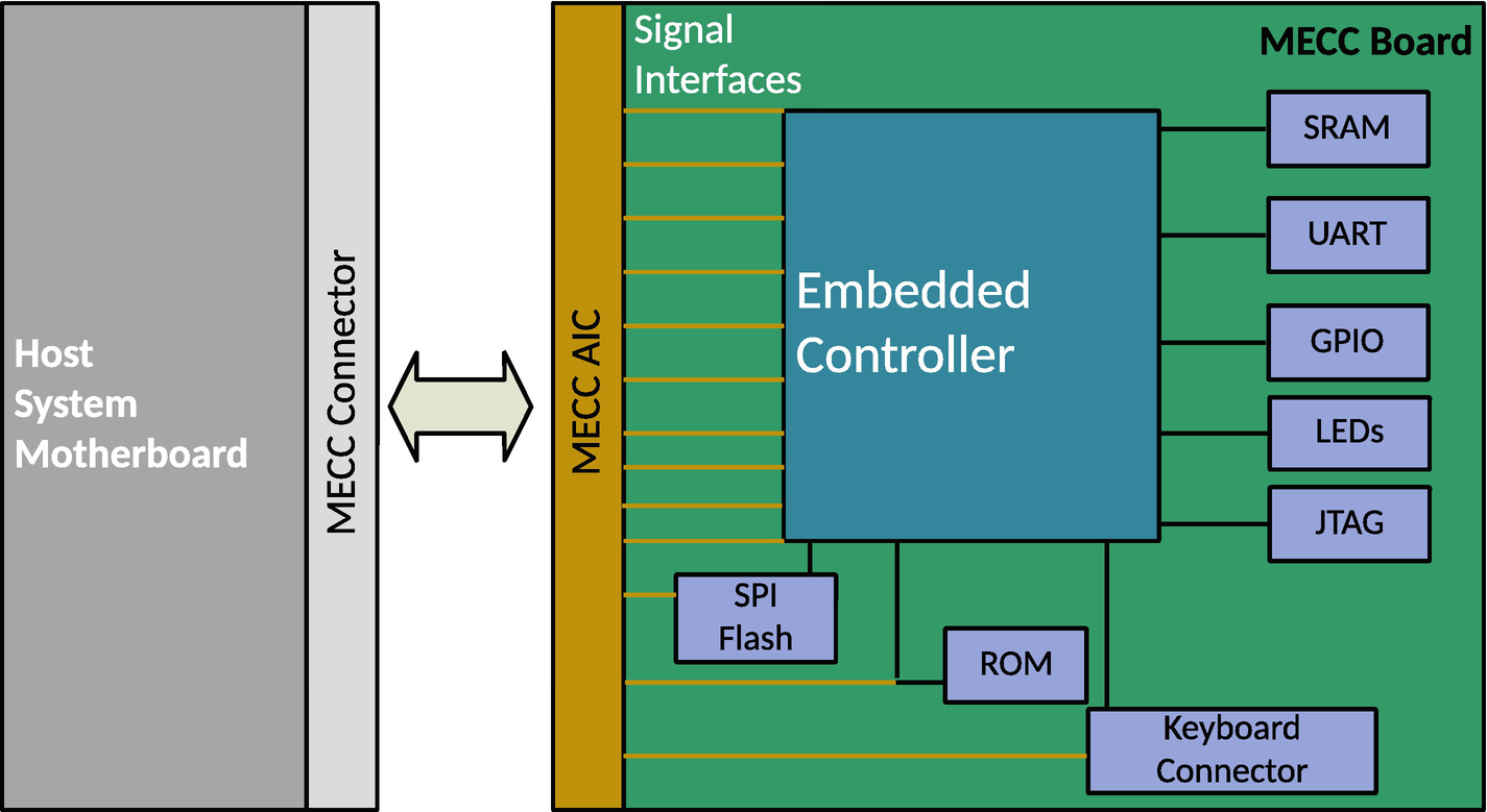
A block diagram depicts the host system motherboard of the M E C C controller connecting with the M E C C A I C of the embedded controller. The M E C C Board has an embedded controller in the middle and connects to various components by signal interfaces.
MECC AIC interfacing with the host system
Open source embedded controller firmware development using Zephyr-OS provides a scalable architecture that enables different MECC cards with different EC SoC vendors. The vendor added Hardware Abstraction Layer (HAL) and EC SoC Board Support Package (BSP) support along with Zephyr RTOS.
Zephyr-Based EC Firmware
The Zephyr OS is a small-footprint kernel that is designed for use on resource-constrained and embedded systems. The kernel has support for cross-architectures and is distributed under the Apache 2.0 license. Zephyr is an open source project managed by the Linux Foundation. Zephyr provides a huge set of features.
Cooperative time slicing: Each thread should intermediately release the CPU to permit the other threads also to execute. It can be achieved using predefined sleep between tasks or explicitly releasing the CPU.
Preemptive time slicing: Use the Zephyr scheduler that allows other threads to get their chance for execution without causing a starvation.
Memory: Zephyr allows the static allocation of memory with a fixed-stack size. It implements memory protection and prevents the EC stack from getting overflowed, having access permission tracking for kernel objects and device drivers. Provides user-space support using MMU/MPU. A platform without MMU/MPU support combines BSP code with a custom kernel to create a monolithic image where both the BSP and the kernel code share the same address space.
Resource definition at compile time: Zephyr ensures all system resources are defined at compile time to reduce the code size and increase performance.
Security: A dedicated team is responsible for maintaining and improving the security. Also, having visibility via the open source development significantly increases the security.
Device tree: The device tree is used to describe the hardware. Information from the device tree is used to perform various device-related operations inside the BSP and/or application layer.

An interface for the host system connects the hardware system with firmware. The Host interface has four layers, namely application, kernel, drivers, S o C definition and Board definition, then Vendor H A L and Cross-Architecture Support, and lastly Platform Hardware.
Zephyr-based embedded firmware architecture diagram
The modular and configurable architecture of ZephyrOS-based embedded controller firmware development is hardware and vendor agnostic. It allows switching the underlying hardware abstraction layer (HAL) and drivers based on different EC SoCs, while the middleware and logic remains intact. To use a different MECC card with different EC SoC vendors, the developer needs to add its HAL and board support package (BSP) to the Zephyr EC firmware repository.
Board | Board-specific code and configuration details. This includes GPIO map, battery parameters, routines to perform board-specific init. |
SoC/vendor-specific HAL | MCU-specific code that deals with lower-level hardware like registers and hardware blocks. |
Drivers | Lower-level drivers for UART, GPIO, Timer, I2C, etc. These drivers are using a device tree and vendor-specific HAL to access the underlying embedded controller hardware block. |
The ZephyrOS layer provides upper-level code that manages the thread, memory management, I/Os management, etc. This includes high-level drivers that publish Zephyr APIs to allow the host interface to access the embedded controller. The host interface defines the hardware link between the embedded controller and host system (PCH and CPU) to work on a computing system. This link can be between LPC or eSPI or I2C, which is the section that covers all the basic applications of EC firmware on an eSPI-enabled platform.
Power Sequencing
System Transitions Between G3->S0 |
|---|
1. The power good (PWRGD) signal to the embedded controller hardware indicates when the main power rail voltage is on and stable. The processor part of the embedded controller will start executing code from the ROM. The boot code is used to download code (user code) from an external flash via the shared flash interface. The downloaded code must configure the device’s pins according to the platform’s need. Once the device is configured for operation, the user code must de-assert the system’s Resume Reset signal (RSMRST#). Any GPIO may be selected for RSMRST# function. The board designer needs to attach an external pull-down on the GPIO pin being used for the RSMRST# function; this will ensure that the RSMRST# pin is asserted low by default. |
2. Perform a deep sleep exit handshake, where PCH sends the SUS_WARN signal to the EC and the EC acknowledges by sending the SUS_ACK signal. |
3. The EC indicates the PCH using the BATLOW signal that there is a valid power source or enough battery capacity to power up the system. |
4. SLP_Sx (where x is based on the supported sleep state of the host system) signals from PCH to the EC indicate that the host system is transiting from the sleep state as per the platform guide. |
5. Wait for ALL_SYS_PWRGD, the all-system power good (ALL_SYS_PWRGD) input generated from the board circuitry indicates to the EC that the SoC power rails are stable. |
6. Based on this, the embedded controller will generate the PWROK signal. |
7. PCH de-asserts PLTRST# after PWROK is stable. The PLTRST# is the main platform reset to other components. |
8. The processor will begin fetching code from the SPI Flash via SPI interface. |
A block diagram flows external circuitry, which connects with an embedded controller that connects with the platform controller hub and then with C P U.
Power sequencing with Zephyr- based EC firmware
Peripheral Management
This section describes the embedded controller managing the human interface device, which mainly handles buttons and switches attached to the motherboard.
Button Array Devices
All sorts of buttons that are present on the motherboard and need human interaction are managed by the embedded controller. For example, the Power Button is the input to EC, which is default-driven high with a pull-up. This signal goes low upon pressing the power button and triggers an interrupt. Apart from that, Volume up/down buttons, Home button, etc., are also being managed by this module.
Switches
This module is also responsible for tracking the state of laptop lid switches and other modules like the screen rotation lock.

A set of three block diagrams. 1, E C firmware application, thread for peripheral management, and register power button for debouncing. 2, E C vendor H A L, G P I O pins, and G P I O Init callback registration. 3, Zephyr O S, G P I O A P I, and G P I O Driver.
Peripheral management with Zephyr-based EC firmware
The embedded controller can be used to detect the docking status of the platform, whether it is in a docking station or not. Based on this status, the EC can perform additional tasks such as switching the system power source to the dock, routing signals from onboard interfaces to the dock, and reporting the docking status to the operating system.
System Management Controller
The section describes the role of the embedded controller as a system management controller, which is used to manage the following items.
Thermal Management
The EC uses the I2C/SMBUS interface to read the platform sensor data, and based on the criticality of the platform state, the EC may have PWM interfaces that can be used to control system fans.
Power Monitoring
The embedded controller ADC signal can be used to monitor the voltage, and based on the usage of the sense resistor, it can also monitor the current consumption of specific power rails. This information could be useful to monitor the battery charging and inform the user or system administrator about any potential problematic power supply condition or detection of a bad charger.
Battery Management
The EC can be used to control the charging of the battery, switch between the battery and AC adapter as the active power source, or monitor the various battery status metrics such as temperature, charging level and battery health, etc.
ACPI Host Interface
The earlier section about “Embedded Controller Interface” provided the required details to understand the host CPU and EC communication using the ACPI host interface. The EC is capable of providing an ACPI-compliant operating system with status and notifications regarding power management events. Also, it is capable of generating wake events to bring the system out from the low-power states.
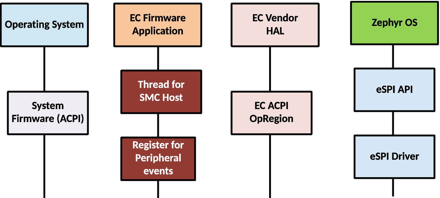
A set of four block diagrams. 1, operating system and system firmware. 2, F C firmware application, Thread for S M C host, Register for peripheral events. 3, E C vendor H A L, E C A C P I Opregion. 4, Zephyr OS, e S P I A P I, e S P I driver
SMC with Zephyr-based EC firmware
Keyboard Controller

A block diagram depicts the operating system P S forward slash 2 drivers, E C firmware application, and Zephyr O S, which passes two layers approach 1 and 2.
KBC with Zephyr-based EC firmware
Keyboard Scan Matrix

A block diagram depicts the operating system P S forward slash 2 driver, E C firmware application, B S P, and zephyr O S in four columns with a description.
Managing a KeyScan event with Zephyr-based EC firmware
This implementation allowed ODM/OEMs to have specific hotkeys as part of the laptop keyboard layout, which is not supported by the international keyboard standard, for example: change screen brightness, enable/disable wireless networking, control audio volume, etc.
To summarize, the embedded controller is a special microcontroller that is part of the majority of mobile computing systems. The firmware that is running on the EC chip is operating at a much higher privilege level, which does various operations that are not possible to perform by even an operating system. This firmware started operating since platform power on and remains active even if the system is at a power-off state; hence, it’s important to ensure the visibility of operations that are running part of the EC firmware. The EC firmware project is being developed with the open source Zephyr OS that has provided visibility into the EC firmware operations. The introduction of Zephyr OS makes EC development easy at the EC vendors and OEMs sides while supporting different EC SoC chips with the same host system using the MECC card.
Summary
This chapter provided an opportunity to understand the different types of firmware that exist and execute on a computing system. Typically, they are categorized as system firmware, device firmware, and manageability firmware. All these types of firmware are running at a higher privilege level compared to the kernel. In this chapter, those privileged levels are being specified as “minus” rings since any vulnerability existing in these layers is tough for any high-level security controller to detect. Hence, this chapter highlighted the need for an open source approach while developing this firmware in the future. This would finally help to restore the trust in the platform and also would provide visibility into the most privileged level firmware, which was not done before.
This chapter proposed two working principles while developing system firmware in the future for embedded systems: hybrid system firmware, where a portion of silicon vendor code is binary and communication with open source firmware is using a standard specification-defined interface, and a true open source system firmware development on an open hardware specification using a modern system programming language such as Rust. Appendix A provides the reasoning behind migrating the system firmware using Rust, an open source system programming language.
Additionally, this chapter specified the well-known mechanism for designing and developing the device firmware using closed source models like option ROM (OpROM). The legacy implementation of the OpROM might increase the platform attack surface. Hence, developing modern OpROM using the open source EDKII source code and toolchain helps to get the initial visibility into the device firmware space, but the ideal goal would be to use the open source firmware model even for developing the device-specific firmware.
The remote management for server platforms and enterprise systems demands out-of-band (OOB) access into the system using a special manageability controller to perform certain tasks when the host system is not available or demands any maintenance. The firmware that is running on these MCUs are at the highest privilege level in the ring and hence always pose the security risk if an intruder had access into the remote system. This chapter provided a brief overview of system architecture of the two widely used microcontrollers, BMC and EC, on the computing system. This will help developers perform a migration to open source firmware development for these manageability controllers in the future.
The goal of this chapter was to explain why firmware architecture is expected to evolve in the future, and it’s fairly possible that the majority of firmware development will migrate to open source. Hence, it’s important that developers understand the industry’s need and prepare themselves for the future.
Chapter 6 represented some innovation in system firmware design and development using an open source firmware approach that addresses the ongoing concerns with extensible firmware architecture that increases the firmware boundary and inherits responsibility while booting the platform.