
1
Flexible All‐Solid‐State Supercapacitors and Micro‐Pattern Supercapacitors
Yuqing Liu1, Chen Zhao2, Shayan Seyedin3, Joselito Razal3 and Jun Chen1
1University of Wollongong, ARC Centre of Excellence for Electromaterials Science, Intelligent Polymer Research Institute, Australian Institute of Innovative Materials, Innovation Campus, Wollongong, NSW, 2522, Australia
2Guangdong University of Technology, School of Materials and Energy, No. 100 Waihuan Xi Road, Guangzhou, 510006, Guangdong, China
3Deakin University, Institute for Frontier Materials, 75 Pigdons Road, Geelong, VIC, 3216, Australia
1.1 Introduction
Research on flexible energy storage devices has received significant attention and has led to the development of novel power sources for various types of flexible and wearable electronics. Currently available energy storage devices are too rigid and bulky for the next generation of flexible electronics. Therefore, the development of high‐performance and reliable power sources that need to be light, thin, and flexible becomes critical. Furthermore, these energy storage devices need to be functional under various mechanical deformations, such as bending, twisting, and even stretching.
To date, progress has been made in developing energy storage systems such as lithium ion batteries and supercapacitors (SCs) for diverse applications in personal consumer electronics, electric vehicles, and uninterruptable power supplies. Lithium ion batteries were commercialized by SONY in 1990 [1]. As illustrated in Figure 1.1, they can achieve an energy density as high as 180 Wh kg−1. However, lithium ion batteries suffer from slow power delivery or uptake, which inhibits their applications in energy storage systems where fast and high power is needed [2]. Conversely, conventional capacitors have a much higher power density than batteries, but their energy density lower. Supercapacitors have the potential to bridge the gap between batteries and conventional capacitors. A typical supercapacitor exhibits an energy density of ∼5 Wh kg−1, which is lower than that of batteries, but a much higher power density of ∼10 kW kg−1 can be achieved in a few seconds. Significant efforts have been made recently to increase the energy density of the supercapacitors to be close to or beyond that of the batteries without sacrificing their high power density.
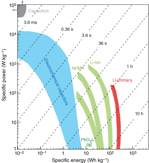
Figure 1.1 Ragone plot for various types of energy storage devices.
Source: Simon and Gogotsi 2008 [1]. Copyright 2008. Reproduced with permission from Nature Publishing Group.
Most studies on supercapacitors have primarily focused on using liquid electrolytes, such as aqueous solutions, organic solutions, and ionic liquids. Since most of these liquid electrolytes are toxic and corrosive, precise packaging is required to avoid any possible leakage of these electrolytes. An alternative solution to the leakage problem, which can also reduce the packaging cost, is the use of a solid‐state electrolyte. Flexible solid‐state supercapacitors present important advantages over traditional ones, which include miniaturization and flexibility, decreased weight, improved energy and power density, and ease of handling. These advantages make them a promising new class of energy storage devices for flexible and wearable electronics.
Supercapacitors are generally classified into two types based on their energy storage mechanisms [1]: (i) electrochemical double‐layer capacitor (EDLC), which stores energy by the adsorption of anions and cations on the surface of electrodes and (ii) pseudocapacitor, which derives the capacitance from the storage of charge in redox materials in response to a redox reaction.
The first EDLC was demonstrated and patented by General Electric in 1957 [3]. Generally, an EDLC is composed of two carbon‐based electrodes with high surface area, an electrolyte, and a separator (Figure 1.2a). When the supercapacitor is charged, cations in the electrolyte move to the negatively polarized electrode, and anions immigrate to the positively polarized electrode. The concept of a double layer was first described by Helmholtz in 1853, who stated that two layers of opposite charge form at the electrode–electrolyte interface. This simple model was then refined by Gouy and Chapman: they introduced a diffuse layer, which arose from the accumulation of ions close to the electrode surface. However, the Gouy–Chapman model overestimated the EDL capacitance since the capacitance increases inversely with the separation distance. Later, Stern combined these two models to define the two parts of ion distribution; the compact layer and the diffuse layer. In the compact layer, the hydrated ions are adsorbed strongly by the electrode, and the compact layer is composed of specifically adsorbed ions and nonspecifically adsorbed counter ions. The diffuse layer is what the Gouy–Chapman model has defined. The capacitance in the EDL can be considered as a combination of the capacitances from the compact and diffuse layers (Figure 1.2b) [5]. The capacitance of an EDLC is generally given by the following Equation (1.1) for a plate capacitor:

Figure 1.2 (a) Schematic structure of an EDLC. . (b) (i) Helmholtz model, (ii) Gouy–Chapman model, and (iii) Stern model of double layer.
Source: Zhang and Zhao 2009 [5]. Copyright 2009. Reproduced with permission from Royal Society of Chemistry.
Source: Zhang and Zhao 2012 [4]. Copyright 2012. Reproduced with permission from John Wiley & Sons
where εr is the dielectric constant of the electrolyte, ε0 is the dielectric constant of vacuum, A is the surface area of the electrode which is accessible to the electrolyte ions, and d is the effective thickness of the double layer. However, some work revealed that the specific capacitance and the surface area do not show a linear relationship [6, 7]. This nonlinearity is ascribed to the presence of some micropores that are inaccessible to large solvated ions. Huang et al. accounted for this pore distribution and separated the capacitance according to pore size [8]. Their models fit well with the experimental results, no matter what type of carbon materials and electrolytes are employed. To date, various carbon materials such as activated carbon, carbon nanotubes (CNTs), and graphene are the most widely used active electrode materials due to their high specific surface area, high conductivity, easy processing, and high chemical stability.
The capacitance of EDLCs strongly depends on the surface area and pore size distribution of the electrode materials. In contrast, a pseudocapacitor stores energy through fast and reversible redox reactions between the electrolyte and the electrode materials. When a potential is applied to a pseudocapacitor, fast and reversible redox reactions occur on the electrode materials and the charge passes across the double layer, resulting in a current passing through the supercapacitor [9]. The typical electrode materials for this kind of supercapacitor include conducting polymers (CPs) [10] and metal oxides or hydroxides [11]. The charging process of conducting polymers can be expressed as follows:
The anions in the electrolytes transfer into the backbone of polymer chains. During discharging, the anions are ejected from the backbone and immigrate into the electrolyte.
Among metal oxides with pseudocapacitance, Ruthenium oxide (RuO2) is the most promising material. This is because it is conductive and has a very high theoretical specific capacitance of ∼2000 F g−12. In acidic electrolytes, the oxidation states of Ru can change from Ru(II) to Ru(IV), which involves rapid reversible electron transfer together with the electron adsorption of protons on the surface of RuO2. This process can be described by the following reaction [9]:
where 0 ≤ x ≤ 2.
1.2 Potential Components and Device Architecture for Flexible Supercapacitors
A flexible solid‐state supercapacitor is generally composed of flexible electrodes, a solid‐state electrolyte, and a flexible packaging material. The flexible electrode should have high capacitance, low self‐discharge, long cycling stability, and high mechanical stability. The solid‐state electrolyte needs to possess high ionic conductivity and good thermal and mechanical stability. The solid‐state electrolyte can also serve as the separator eliminating the need for an additional separator [12].
1.2.1 Flexible Electrode Materials
1.2.1.1 Carbon Materials
Carbon nanomaterials such as 1D CNTs and 2D graphene, with structures composed of conjugated sp2 carbons, have been widely studied for flexible energy storage applications.
CNTs are tubular allotropes of carbon with graphitic structures (Figure 1.3). They can be classified into two types: single‐walled carbon nanotubes (SWCNTs) and multiwalled carbon nanotubes (MWCNTs)14. CNTs have attracted significant interest in recent years for developing high‐performance flexible supercapacitors due to their high electrical conductivity, unique pore structure, and good mechanical stability [15]. CNTs possess moderate specific surface area compared to activated carbons; however, comparable specific capacitance has been reported for CNTs. Niu et al. reported a MWCNT‐based electrode that exhibited a maximum specific capacitance of ∼110 F g−116. SWCNT‐based electrodes achieved a specific capacitance as high as 180 F g−117. Recent studies have shown that aligned CNTs are more efficient in ion transportation compared to the randomly entangled CNTs. A high specific capacitance of 365 F g−1 has been obtained for an MWCNT array based electrode [18].

Figure 1.3 Schematic structures of (a) SWCNT and (b) MWCNT.
Source: Martins‐Júnior et al. 2013 [13]. Copyright 2013. Reproduced with permission from SAGE.
Graphene, a one‐atom thick single‐layer graphitic carbon (Figure 1.4), has also attracted significant attention as electrode materials for flexible supercapacitors because of its high electrical properties, large surface area, and high mechanical strength [20–23]. The theoretical specific surface area of graphene is about 2630 m2 g−124, leading to the theoretical double‐layer capacitance of 550 F g−125. However, this high level of capacitance is difficult to achieve as the result of the restacking of the graphene sheets during the electrode preparation process. Stoller et al. investigated reduced graphene oxide (rGO) as electrode materials [24]. The individual graphene sheets partially agglomerated during the reduction process, leading to moderate specific capacitances of 135 and 99 F g−1 in aqueous and organic electrolytes, respectively. Zhu et al. reported that KOH‐activated graphene could achieve a specific surface area of up to 3100 m2 g−1, resulting in a specific capacitance of 166 F g−1 at a current density of 5.7 A g−126.

Figure 1.4 Schematic structure of one single‐layer graphene.
Source: Yan et al. 2012 [19]. Copyright 2012. Reproduced with permission from Royal Society of Chemistry.
1.2.1.2 Conducting Polymers
Conducting polymers are organic polymers that can conduct electricity. In 2000, the Nobel Prize in Chemistry was awarded to Alan J. Heeger, Alan MacDiarmid, and Hideki Shirakawa for their outstanding work on conducting polymer polyacetylene [27]. During the past decades, numerous CPs have been developed, and have found widespread application in polymer light‐emitting diodes (LEDs) [28], sensors [29], artificial muscles [30], anticorrosion coatings [31], and in energy conversion and storage devices [10, 32]. CPs are suitable as electrode materials for flexible supercapacitors as they possess many advantages: low cost, environmental friendliness, high conductivity in the doped state, high capacitance, ease of synthesis, and the possibility of manufacturing them as self‐supporting and flexible thin films 10, [33–36]. The most commonly studied CPs in supercapacitors are polypyrrole (PPy) [37], polyaniline (PANi) [35], and derivatives of polythiophene (PTh), such as poly(ethylenedioxythiophene) (PEDOT) [38]. The structures of the common CPs are shown in Figure 1.5.
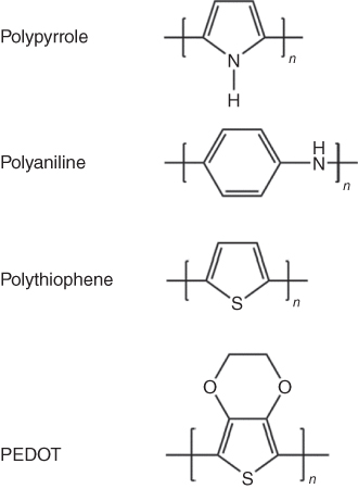
Figure 1.5 Chemical structures of PPy, PANi, PTh, and PEDOT (undoped form).
CPs can be p‐doped (with anions) or n‐doped (with cations). Electrochemical p‐doping of conducting polymer occurs by removing electrons from the polymer chain and the addition of anions to the polymer backbone to balance the positive charge. The reverse mechanism (i.e. the addition of electrons to the backbone and balancing the negative charge with cations) accounts for the electrochemical n‐doping of conducting polymers. PPy and PANi can only be p‐doped in supercapacitor systems due to the highly negative potentials required for n‐doping, which is beyond the reduction potential limit of the electrolyte [39]. PTh and its derivatives can be both p‐doped and n‐doped [40, 41].
Electrodes made from CPs showed much higher specific capacitances compared to carbon materials. Fan and Maier prepared a highly porous PPy electrode on Ti foil using the cyclic voltammetry (CV) method [42]. The resultant PPy showed a specific capacitance of about 450 F g−1. PPy doped with Nafion ions or perchlorate exhibited a specific capacitance of 344 or 355 F g−1, respectively [43]. PANi was reported to show a specific capacitance higher than 500 F g−144–54]. A derivative of PTh, poly(tris(4‐(thiophen‐2‐yl)phenyl)amine), can even achieve a specific capacitance greater than 990 F g−155. The drawback of the CPs‐based electrodes is that they suffer from structural degradation caused by swelling and shrinking of CPs during long‐term cycling, leading to the decay of their electrochemical performance. It is suggested that electrodes prepared from nanostructured CPs [56] or composites of CPs with carbon‐based materials [57–59] can show superior cyclic stabilities.
1.2.1.3 Composite Materials
Carbon materials, such as CNTs and graphene, can be employed as a conducting substrate for the integration of pseudocapacitive materials to boost the electrode performance [60]. The combination of carbon materials with conducting polymers has been proven to be effective for preparing electrodes for supercapacitors due to the synergistic effect of electrochemical double‐layer capacitance and pseudocapacitance61. This strategy endows the CPs with improved cyclic stabilities as carbon materials such as CNTs and graphene can act as frameworks to stabilize the CPs, limiting their swelling and shrinking during the cycles [62]. Apart from CPs such as PPy [63, 64], PANi [65, 66], and PEDOT [67], various metal oxides, including MnOx68, 69], RuO270, V2O571, and Co3O472 have also been explored for the fabrication of flexible carbon‐based composite electrodes.
1.2.2 Solid‐State Electrolytes
The use of solid‐state electrolytes addresses the electrolyte leakage issue, and also facilitates the device‐packaging process. The most widely used solid‐state electrolytes in supercapacitors are polymer electrolytes. The ideal polymer electrolytes should be of high ionic conductivities at room temperature, low electronic conductivities, and good mechanical stabilities. The polymer electrolytes typically achieve their ionic conductivities through the movement of protons, lithium ions, or the ionic species in ionic liquids [73].
Proton‐conducting polymer electrolytes, composed of acid/polymer blends are most widely used solid electrolytes for flexible supercapacitors. The main polymer used in this system is poly(vinyl alcohol) (PVA), and H2SO4 and H3PO4 are often chosen as the proton conductors 64, [74–77]. This type of polymer electrolytes is typically prepared by the addition of an acid to the aqueous polymer solution. Freestanding electrolyte films, which exhibit conductivity in the range of 10−6–10−3 S cm−1, can then be obtained by evaporating the water. During the cell‐assembling process, the electrodes are immersed in the hot polymer electrolyte solution or the electrolyte solution is cast on the electrode surface. The polymer electrolyte solution can penetrate the active layer of the electrodes, increasing the electrochemically active surface area [73]. After drying, two electrodes with polymer electrolyte are pressed face‐to‐face to form an integrated cell. Proton‐conducting polymer electrolytes exhibit the highest conductivity among all polymer electrolytes. They can be prepared and used under ambient conditions and the presence of water helps to maintain high conductivity. However, their main drawback is the relatively narrow voltage window (usually limited to 1 V) [73].
Lithium‐ion‐conducting polymer electrolytes are generally prepared by mixing a polymer, such as poly(ethylene oxide) (PEO), poly(acrylonitrile) (PAN), poly(methyl methacrylate) (PMMA), and poly(vinylidene fluoride) (PVDF) with a lithium salt dissolved in an organic solvent. Solvents such as ethylene carbonate (EC), propylene carbonate (PC), ethyl methyl carbonate (EMC), dimethyl carbonate (DMC), diethyl carbonate (DEC), dimethyl formamide (DMF), and tetrahydrofuran (THF) were found to also act as a plasticizer giving rise to a higher conductivity [78]. Lithium‐ion‐conducting polymer electrolytes are prepared by dissolving various lithium salts in organic solvents and immobilizing in a polymer matrix. The lithium‐ions‐based solid electrolytes can operate in a wide electrochemical window. However, they are moisture sensitive and require oxygen and moisture‐free environment for cell assembling.
Ionic liquids are a class of liquid slats. Their unique properties, such as low volatility and flammability, high thermal stability, and wide potential window, make them suitable electrolytes for supercapacitor application [79]. They can be trapped in a polymer matrix or a silica network, form an ion gel that can be used as solid electrolytes [80–83].
1.2.3 Device Architecture of Flexible Supercapacitor
The electrochemical performance of a supercapacitor, is dependent not only on the properties of the materials used in each component, but also on how these components are designed, matched, and combined to form a device that can satisfy the performance requirements. Here, we discuss two widely studied architectures used for flexible supercapacitor (fSC) devices: sandwiched stacked structure and interdigitated planar structure 84–86] (Figure 1.6).

Figure 1.6 Schematic diagrams of flexible supercapacitors with (a) conventional sandwiched structure and (b) interdigitated structure.
The early all‐solid‐state fSCs adopted the conventional sandwiched structure design with a stacked configuration of current collector/film electrode/solid electrolyte/film electrode/current collector (Figure 1.6a). This design attracted the attention of researchers due to its extremely simple structure and relatively easy fabrication process. However, when the thicker electrodes are required, this design often suffers from serious ion transport limitations due to the consequently increased ion transport path [84, 87]. Moreover, portable electronic devices should not only be flexible, but also need to have small size and thickness. Consequently, the bulky sandwiched architecture is not compatible with the planar geometry of the miniaturized microelectronics and not suitable for electronic circuitry [84].
To overcome this problem, a planar design with several microelectrodes (as each electrode) interdigitally arranged on a flexible substrate such as terephthalate (PET) or polyimide (PI) films or papers (interdigitated design), was developed as a new emerging device structure (Figure 1.6b) [84]. The fabrication of interdigitated microelectrodes often involves an additional micro‐patterning step before or after film electrode deposition. Compared with the stacked sandwiched structure, the plannar interdigitated structure possesses the following advantages:
- Space‐saving device. Without a layer of solid electrolyte used as separator in the sandwiched design, the fSC device with interdigitated design is thinner and smaller and can store and provide more power in a limited space without the volume being wasted on the separator layer.
- Shorter ion transport paths. The advances in micro‐patterning techniques make it possible to accurately control very small distances between adjacent electrodes thereby shortening the ion transport path. This results in decreasing the ion transport resistance, increasing the rate capability and power density of the device.
- Better penetration of electrolyte ions. The increased exposure of the microelectrodes to the electrolyte in the interdigitated design can increase the ion accessibility of the inner surface of the electrode materials resulting in an improved energy storage.
- Facile interconnection and integration within the electronic systems. Most applications require a current or voltage that is higher than what can be delivered by a single SC device. Hence, the connection of the SC devices in series, parallel or a combination of those are needed. Having the electrodes in the same plane would facilitate these connections on one chip, avoiding the intricate wired interconnection between sandwiched SCs [88].
The drawbacks of the interdigitated design are as follows:
- Less areal energy. The footprint area of the interdigitated SCs includes the active surface areas of both electrodes and an inactive gap surface in between, while the footprint area of the sandwiched SCs is only defined by the active materials. Hence, a higher areal energy can be achieved for SCs in the sandwiched configuration. The adverse impact of the interdigitated SCs can be minimized by decreasing the distance between the adjacent electrodes. However, it normally involves more expensive micro‐fabrication techniques with fine control on resolution.
- Additional consumption of expenses and labor in the patterning step. This is the main challenge for the scale‐up of the interdigitated design for commercial applications. Efforts are being devoted to develop scalable micro‐fabrication techniques for various electrode materials, which will be discussed in Section 1.3.2.
Sandwiched SCs are still the industrially favorable device design due to their facile and low‐cost fabrication process, although the interdigitated structures show many advantages. However, with the development of the miniaturized wearable electronics and the continuous progress in micro‐patterning techniques, the interdigitated SCs may find an increased application.
1.3 Flexible Supercapacitor Devices with Sandwiched Structures
1.3.1 Freestanding Films Based Flexible Devices
Flexible supercapacitor devices can be fabricated from freestanding electrode films. One of the active materials used in preparing flexible and freestanding electrodes is CNT. CNTs can be assembled into freestanding films through vacuum filtration‐induced self‐assembly. In a typical process, the stable CNT dispersion is first formed by breaking up the large bundles of CNTs in water (with the aid of a surfactant) or in organic solvents using ultrasonic energy. During the filtration process, CNTs are trapped inside or on the surface of the membrane pores, forming an interconnected and entangled film. The CNT film can then be peeled off after sufficient film thickness has been achieved [89]. Aligned CNT films can also obtained by drawing the vertically oriented CNT arrays [90]. Such aligned CNT films are ultrathin, transparent, stretchable, and conductive. Chen et al. [91] developed a transparent and stretchable supercapacitor electrode by continuously drawing a transparent CNT sheet out from a CNT forest onto a poly(dimethylsiloxane) (PDMS) substrate and then coating a PVA/H3PO4 polymer electrolyte solution onto the CNT sheet. The flexible supercapacitor device was made by assembling two electrodes in either a parallel or cross configuration (Figure 1.7a). The transparent supercapacitor showed a specific capacitance of 7.3 F g−1 and can be bent or biaxially stretched to 30% without noticeable changes in its electrochemical performance (Figure 1.7b–d).
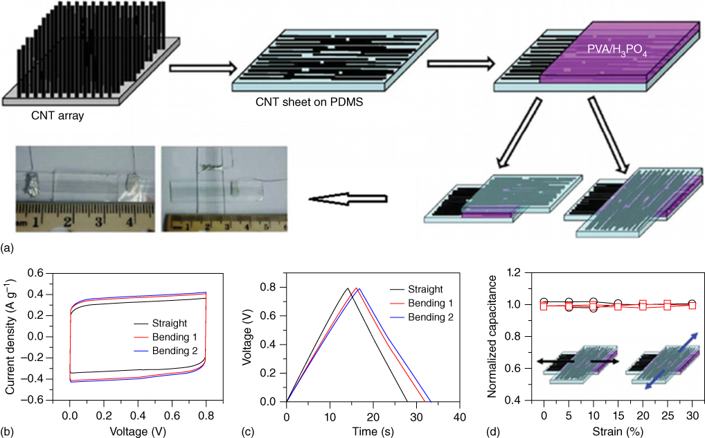
Figure 1.7 (a) Schematic illustration of the process for fabricating the transparent and stretchable supercapacitor. (b) CV curves (at scan rate of 0.1 V s−1), and (c) charge–discharge curves (at constant current density of 0.2 A g−1) of the supercapacitor under different states. (d) Normalized specific capacitance of the supercapacitor as a function of tensile strain.
Source: Chen et al. 2014 [91]. Copyright 2014. Reproduced with permission from Nature Publishing Group.
Freestanding graphene films or papers, have also shown great promise as flexible electrodes for supercapacitors because they are ultrathin, flexible, and lightweight. Graphene films have been fabricated through various solution processing methods, such as vacuum filtration, spin‐coating, Langmuir–Blodgett, layer‐by‐layer deposition, and interfacial self‐assembly [92]. However, during the fabrication process, the graphene sheets tend to aggregate and restack due to the strong π – π interactions and van der Waals forces, limiting the available surface area and the diffusion of electrolyte ions, resulting in deteriorating electrochemical performance. To prevent the restacking of graphene sheets, two main strategies have been proposed: (i) to add spaces such as CNTs and polymers [93–95] and (ii) to produce 3D porous graphene networks [96, 97].
Shi and coworkers [94] fabricated a flexible electrodes from rGO /poly(vinyl pyrrolidone) (PVP) composite film (Figure 1.8a,b). The PVP chains were found to effectively intercalate between the graphene sheets, acting as spacers to prevent the graphene sheets restacking. The composite films showed a high mechanical strength of ∼121.5 MPa (Figure 1.8c). The solid‐state supercapacitors based on the rGO/PVP composite containing 55% rGO (by weight) showed high volumetric specific capacitances (67.4 F cm−3 at 1 A g−1), good rate‐capability (51.4 F cm−3 at 100 A g−1), and excellent flexibility (Figure 1.8d). Park and coworkers [95] prepared Nafion functionalized rGO films using a supramolecular assembly approach and vacuum filtration. The integration of Nafion not only prevented the restacking of graphene sheets, but also improved the interfacial wettability between the electrodes and electrolyte. All‐solid‐state supercapacitors were fabricated by sandwiching Nafion membranes between the functionalized rGO thin films. The specific capacitance of functionalized rGO was 118.5 F g−1, which is about two times higher than the reported value for the pure rGO (62.3 F g−1). After bending at a radius of 2.2 mm, the CV curves of the supercapacitor exhibited almost the same shape as those in the flat state, indicating high mechanical flexibility.
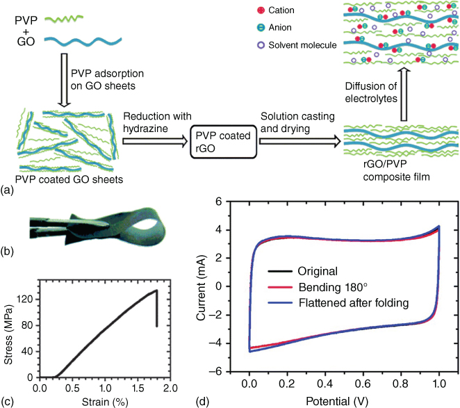
Figure 1.8 (a) Schematic illustration of fabrication of rGO/PVP composite film and the diffusion of the electrolyte onto the surfaces of rGO sheets. (b) Photograph and (c) tensile stress–strain property of the flexible rGO/PVP film. (d) CV curves of the solid‐state device based on the rGO55/PVP45 composite film with a thickness of 2.4 μm in various bending states (scan rate = 100 mV s−1).
Source: Huang et al. 2014 [94]. Copyright 2014. Reproduced with permission from Royal Society of Chemistry.
Tremendous attention has also been paid to 3D porous graphene network to prevent the aggregation of the graphene sheets. The general approaches involved include freeze drying [98], hydrothermal [96], and organic sol–gel [99]. Shu et al. [97] prepared a flexible freestanding 3D graphene with interconnected porous structure by freeze drying a wet GO gel, followed by thermal and chemical reduction (Figure 1.9a). The water in the precursor GO gel helped to prevent the restacking of the graphene sheets. The porous graphene paper was highly flexible (Figure 1.9b). A flexible solid‐state supercapacitor was fabricated using those graphene papers and PVA/H2SO4 polymer electrolyte (Figure 1.9c,d). The graphene paper in the device delivered a specific capacitance of 137 F g−1 at 1 A g−1. And it can maintain 94% of its capacitance under bending (Figure 1.9e). 3D graphene macrostructures such as graphene hydrogelscan also be prepared by a one‐step hydrothermal process. Xu et al. [96] pressed the hydrothermally reduced graphene hydrogel onto gold coated polyimide substrate with a PVA/H2SO4 polymer electrolyte to assemble flexible solid‐state supercapacitors The graphene gel film in the solid‐state device achieved a high specific capacitance of 186 F g−1 at 1 A g−1, and the device showed stable electrochemical performance under different bending angles.
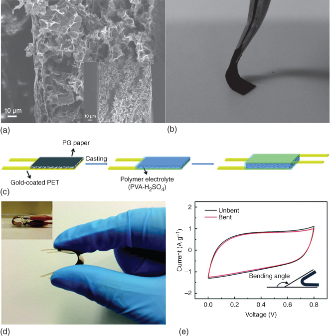
Figure 1.9 (a) Cross‐sectional SEM image of a porous graphene paper. (b) Photograph of the porous graphene paper demonstrating its flexibility. (c) Schematic procedure to fabricate a solid‐state supercapacitor from porous graphene paper. (d) Photograph of the flexible device at a bending state. (e) CV curves of the flexible device at bending and relaxation state (scan rate = 10 mV s−1).
Source: Shu et al. 2015 [97]. Copyright 2015. Reproduced with permission from Royal Society of Chemistry.
Apart from the wet process to create 3D graphene structures, Kaner's group used a standard LightScribe CD/DVD drive and developed a solid‐state laser scribed strategy to produce 3D porous graphene electrodes (Figure 1.10) [100]. The laser irradiation reduced the GO to laser‐scribed graphene (LSG), and the initially stacked GO sheets were converted to well‐exfoliated graphene (EG) sheets. The obtained LSG films showed excellent conductivity (1738 S m−1) and mechanical flexibility (1% change in the electrical resistance after 1000 bending cycles). Flexible solid‐state supercapacitor based on the LSG films and PVA/H3PO4 electrolyte showed comparable performance with those used H3PO4 as the liquid electrolyte. Bending had almost no effect on the capacitive behavior of the device, and only ∼5% change in the device capacitance was observed after 1000 bending cycles.

Figure 1.10 (a–d) Schematic illustration of the fabrication of LSG. (e) SEM images of GO and LSG. Schematic of (f) a conventional structured device and (g) a solid‐state device based on LSG (Inset in (g) indicates the flexibility of the device). (h) CV curves of the devices at different bending angles.
Source: El‐Kady et al. 2012 [100]. Copyright 2012. Reproduced with permission from American Association for the Advancement of Science.
Compared to pure carbon based materials, pseudocapacitive materials exhibit higher specific capacitance. They have been incorporated into the carbon based flexible electrodes to fabricate solid‐state supercapacitors with a higher electrochemical performance. For example, Meng et al. [77] developed a solid‐state paper‐like supercapacitor based on PANi coated free‐standing CNT film and PVA/H2SO4 gel electrolyte. This device showed a specific capacitance of 31.4 F g−1 and excellent cycling stability.
1.3.2 Flexible Substrate Supported Electrodes Based Devices
Another approach to fabricate flexible solid‐state supercapacitor is to use flexible substrate to support the electrodes. Mechanically flexible, thin, and lightweight plastics such as polyethylene terephthalate (PET) have been widely used as the supporting substrates for flexible supercapacitors. Kaempgen et al. [101] demonstrated a thin film supercapacitor based on spray coated SWCNT networks (served as both electrode and current collector) on a PET substrate using a PVA/H3PO4 gel electrolyte (Figure 1.11a,b). The SWCNT network showed a specific capacitance of ∼36 F g−1 in the solid‐state device. Chen et al. [102] reported a transparent solid‐state stretchable supercapacitor based on wrinkled graphene electrodes that can sustain a strain of up to 40% (Figure 1.11c,d). The wrinkled graphene was synthesized by chemical vapor deposition (CVD) on a wrinkled copper film. After PDMS coating and etching, the wrinkled graphene was well transferred onto PDMS. The solid‐state supercapacitor showed a stable performance over hundreds of stretching cycles.
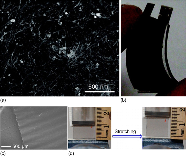
Figure 1.11 (a) SEM image of the SWCNT network. (b) Photograph of an SWCNT network based flexible supercapacitor. (c) SEM images of the wrinkled graphene film. (d) Photographs of the wrinkled graphene‐based flexible supercapacitor device at different stretching states.
Source: Chen et al. 2014 [102]. Copyright 2014. Reproduced with permission from American Chemical Society.
Source: Kaempgen et al. 2009 [101]. Copyright 2009. Reproduced with permission from American Chemical Society.
Although solid polymeric substrates have been widely used as flexible substrates, they suffer from limited active materials loading and diffusion of electrolyte. Alternatively, porous substrates, such as paper and textile, have been used for flexible supercapacitors. In some cases, only the surface of the papers is made conductive, and the bulk of papers act as a flexible support. Yao et al. [103] introduced a pencil‐drawing and a subsequent PANi electrodeposition to fabricate graphite/PANi hybrid electrodes on a paper. The hybrid electrode was made by first drawing a conductive graphite layer on a paper using a pencil. Electrochemical deposition of PANi nanowire networks was then carried out on the graphite layer. The solid‐state supercapacitors was assembled by two graphite/PANi electrodes sandwiching a PVA/H2SO4 electrolyte layer and achieved a high energy density of 0.31 mWh cm−3 at a power density of 0.054 W cm−1. Liu et al. [104] demonstrated PANi‐rGO‐cellulose paper nanocomposite electrodes. The fabrication of nanocomposite electrodes started with coating a GO layer on the cellulose fibers in the paper, and then the GO‐coated cellulose fiber paper was used as a template to assemble porous rGO networks in the pores of the paper by a hydrothermal process. PANi was then chemically polymerized on the rGO paper to obtain PANi‐rGO/paper composite paper (Figure 1.12a). The solid‐state supercapacitor was assembled by sandwiching two such composite papers with PVA/H2SO4 polymer electrolyte (Figure 1.12b). The calculated specific capacitance of PANi‐rGO/paper electrode was about 224 F g−1, and the solid‐state device showed stable performance at folding and bending states (Figure 1.12c–e).

Figure 1.12 (a) Schematic diagram of the preparation of the PANi‐rGO/cellulose fiber composite paper. (b) Schematic diagram of an all‐solid‐state integrated supercapacitor device. (c) CV curves of the all‐solid‐state supercapacitor under different deformation conditions (scan rate: 2 mV s−1). Normalized specific capacitance of the all‐solid‐state supercapacitor under (d) bending and (e) folding states.
Source: Liu et al. 2014 [104]. Copyright 2014. Reproduced with permission from John Wiley & Sons.
Textiles have hierarchical porosity in the fibers and yarns, and there is also free space between fibers and yarns. Such inherently porous structures facilitate the accommodation of active materials. Yun et al. [105] designed a solid‐state stretchable textile supercapacitor using PPy‐MnO2/CNT coated textile electrodes and PEO‐based gel electrolyte. A piece of textile made of cotton was dipped into SWCNT ink to obtain a conductive textile, MnO2, and PPy was then electrodeposited on the SWCNT‐coated textile. The textile supercapacitor exhibited an energy density of 31.1 Wh kg−1 and a power density of 22.1 kW kg−1. The textile device showed a stable electrochemical performance under bending and stretching deformations. Highly conductive carbon cloths were also employed as substrates as an alternative for flexible textile supercapacitor fabrication. For instance, Yuan et al. [106] fabricated a solid‐state supercapacitor using a carbon cloth as a current collector and mechanical support for the carbon nanoparticles/MnO2 nanorods hybrid electrode and PVA/H3PO4 electrolyte (Figure 1.13a). The device showed an excellent electrochemical performance with an energy density of 4.8 Wh kg−1 at a power density of 14 kW kg−1. The device could be bended without scarifying its performance (Figure 1.13b).

Figure 1.13 (a) Photographs of the solid‐state supercapacitor made of carbon nanoparticles/MnO2 nanorods hybrid electrode and a carbon cloth at normal, bent, and twisted state. The image on the right shows a red LED turned on by three supercapacitors connected in series. (b) CV curves for the solid‐state supercapacitor at different bending angles.
Source: Yuan et al. 2012 [106]. Copyright 2012. Reproduced with permission from American Chemical Society.
1.4 Flexible Micro‐Supercapacitor Devices with Interdigitated Architecture
The fabrication of flexible microsupercapacitors with interdigitated design involves a micro‐patterning step before or after the flexible film electrode formation. Recent developments in micro‐manufacturing technology have opened pathways for the patterning step of the microsupercapacitor fabrication that suit the type of active materials and the required performance (either high energy density or high power density). The fabrication methods can be mainly classified into three categories: in situ synthesis of active materials on a pre‐patterned surface, directly printing of existing active materials, and patterning the well‐developed film electrode.
1.4.1 In situ Synthesis of Active Materials on Pre‐Patterned Surfaces
Active materials can be synthesized on the pre‐patterned surface via various synthesis techniques (such as electrochemical polymerization [107, 108], electrolytic deposition [109, 110], electrophoretic deposition [88], chemical deposition [111], etc.). Here, a pre‐patterned surface is firstly prepared by coating and patterning a thin layer of photoresist (PR) or removable inks on a flexible substrate. In the next step, the current collectors are coated on the flexible substrate using the patterned PR or ink as the mask followed by the deposition of the active material. The masks are then removed chemically either before or after the active materials deposition, whenever they are no longer needed.
Sung et al. [107] reported a PR patterning using the conventional photolithography technique which was the earliest and the most common method of mask preparation for the current collector coating. In this approach, a patterned interdigitated gold microelectrode was first prepared on a silicon wafer by photolithography. PPy was then electrochemically polymerized on the pre‐patterned gold layer. In the next step, a layer of solidified PVA‐H3PO4 gel electrolyte was firmly attached to the PPy microelectrode arrays. Upon detaching both PPy and the electrolyte layer from the silicon substrate, a small, lightweight, freestanding, and flexible microsupercapacitor (fMSC) device was achieved. A relatively poor electrochemical performance (with areal capacitance of the device <0.5 mF cm−2) was observed for this fMSC device emanating from the primitive device assembly technique such as the lack of current collectors and inappropriate coating of the electrolyte (simply attaching the dried gel electrolyte film to the electrode materials). Nevertheless, this study demonstrated the feasibility of fabricating flexible all‐solid‐state microsupercapacitor devices.
Using similar techniques (photolithography and in situ chemical polymerization), Wang et al. [111] further modified and improved the fabrication steps of fMSCs (Figure 1.14). They directly prepared PANi‐based microelectrodes with Au/Cr as the current collector on a flexible PET film as the substrate compared to the silicon wafer. Moreover, instead of attaching a layer of the solidified electrolyte on active materials, the PVA‐H2SO4 gel electrolyte was drop‐cast on the surface of the microelectrodes and then solidified. Taking the advantage of the advanced nanostructure of PANi electrodes, existence of current collectors, and better penetration of the electrolyte, the as‐prepared fMSCs exhibited an excellent device capacitance of 1.17 mF cm−2 and 25.4 F cm−3 (23.52 mF cm−2 and 588 F cm−3 for electrode materials), a high scan rate capability (>10 V s−1), and a low leakage current. In addition, the feasibility of increasing the operating voltage and/or current by simply making series and/or parallel connecting circuits of MSC units on one PET film was firstly demonstrated. This is important in industrial applications where the required voltage or current is typically higher than what one single fMSC can supply. Following this approach, not only conducting polymers but carbon materials such as rGO [88], CNT [82], and metal oxides [112] were also fabricated. Despite the high resolution of the prepared interdigitated microelectrodes (minimum width of array ∼50 μm) and the excellent fMSCs device performance, the high cost and the sophisticated process of photolithography limited its further development toward commercialization.

Figure 1.14 A schematic of fabrication process for interdigitated microelectrodes of PANi nanowire arrays on a flexible film.
Source: Wang et al. 2011 [111]. Copyright 2011. Reproduced with permission from John Wiley & Sons.
Commercial and printable inks can also be used as the mask material instead of PR. Using a common office laser printer, Ye's group printed a circuit template as a mask on a PET film [108, 110]. They deposited Au/PANi and Au/MnO2/Au (AMA) stacked microelectrodes, respectively, on the mask by beam evaporation of Au current collectors and the electrodeposition of the active materials (Figure 1.15a–h). The fMSC devices were achieved by lifting off the printed circuit template using THF. As the circuit pattern can be designed on a personal computer using software, the dimension parameters and the number of patterns could be easily adjusted. Hundreds of patterns can be printed on a flexible PET film (Figure 1.15j,k) indicating the great potential of this approach for scalable fMSCs fabrication. Jiang et al. used a Marker Pen Lithography technique, in which writing sacrificial ink patterns were written using commercial marker pens on the substrate and were used as the mask for the deposition of current collectors and active materials (PEDOT and PANi) [113]. Despite the relatively low resolution (minimum printed width >250 μm for laser printer, ∼500 μm for maker pen) that needs to be improved using a more precise printer to achieve higher device performance, the simplicity of these innovative strategies opened up new avenues for easy and scalable fabrication of fMSCs.
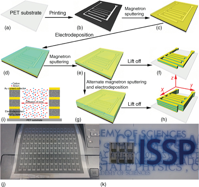
Figure 1.15 (a–h) Schematic illustrations of the fabrication procedure for the on‐chip fMSCs with AMA stacked hybrid electrodes and single AMA sandwiched hybrid electrode units. (i) Schematic diagram of the ion diffusion pathway in the AMA stacked hybrid electrodes. (j) A photograph of a large area of printed interdigitated patterns on a flexible PET film. (k) A photograph of the as‐prepared on‐chip fMSCs with AMA stacked hybrid electrodes.
Source: Hu et al. 2016 [110]. Copyright 2016. Reproduced with permission from John Wiley & Sons.
The fMSCs prepared from pseudocapacitive electrode materials showed superior areal and volumetric capacitances (9–41 mF cm−2 and 50–147 F cm−3 respectively) compared to the relatively low capacitance of the carbon‐based fMSCs (<1 mF cm−2 and <20 F cm−3 respectively) normalized by the area and volume of the whole device. The poor performance of carbon‐based devices can be explained by the ultrathin thickness (∼25 nm to ∼1 μm) of the in situ synthesized active materials, as carbon‐based materials have poorer adhesion to the current collectors and substrates than pseudocapacitive materials. Meanwhile, the relatively low intrinsic volumetric capacitance exacerbates the poor areal capacitance of the ultrathin carbon‐based device [87]. Also, some of the techniques used for the in situ deposition of carbon materials (such as electrostatic spray deposition of GO/CNT [114], CVD of graphene [115] and CNT [116], etc.) require stringent conditions, e.g. relatively high temperature, that may not be compatible with the commonly used low‐cost PET and paper substrates used in fMSCs fabrication. In addition, the post‐processing of carefully and fully removing PR residual or ink masks is labor‐intensive and may result in losing some of the active materials. These limitations motivated the researchers to seek alternative ways for the preparation of carbon‐based fMSCs.
1.4.2 Direct Printing of Active Materials
Direct printing of inks containing active materials onto a flexible substrate is another approach by which microelectrodes can be fabricated for use in fMSCs. Starting from the carbon materials powders, a stable suspension or a viscous slurry is obtained first. A binder, surfactant, and/or conductive additives may also be added to the suspension to improve the printability and/or conductivity of the active materials. Compared to the sophisticated steps required in the preparation of microelectrodes using the pre‐patterning approach, the direct printing of the active materials can realize the deposition and patterning simultaneously in one step, thus reducing materials usage and process complexities. Different printing techniques (such as inkjet printing [15–17, 117–119], extrusion printing [18, 120], screen printing [13, 20, 121, 122], roll‐to‐roll printing [21, 22, 123, 124], etc.) have been exploited to prepare patterned microelectrodes from carbonaceous materials to make fMSCs. Highly dispersed and stable active materials with suitable particle sizes and appropriate rheological properties are required for successful patterning using printing techniques.
In screen printing, the ink is forced through a screen with pre‐patterned open meshes and then contact with the substrate (Figure 1.16a). Screen printing can be carried out in a large scale with uniform thickness and within a short period. It also allows for patterning on a variety of substrates, not only on a smooth plastic film, but also on porous cloth and papers. Screen printing has enabled the integration of various composite active materials with superior nanostructures into fMSCs, which were incompatible with other fabrication strategies. For instance, using screen printing techniques, Wang et al. fabricated MnO2/onion‐like carbon (MnO2/OLC)‐based fMSCs, in which the MnO2/OLC nanocomposites have unique nanourchin shapes with the diameter of 200–500 nm [125]. The optimized device exhibited high areal and volumetric capacitances of ∼7.04 mF cm−2 and ∼7.04 F cm−3. Similarly, Zhu et al. screen printed interdigitated electrodes using the ink of novel 3D nanocomposites consisting cobalt oxide (CoO) nanoflowers woven with CNTs networks [121]. High volumetric and areal capacitances of ∼17.4 F cm−3 and ∼17.4 mF cm−2, respectively, and a high energy density of ∼3.48 mWh cm−3 were achieved for the fMSC device. In another study, nitrogen‐doped graphene was screen printed at a relatively high electrode thickness of ∼10 μm achieving a high areal capacitance of ∼3.4 mF cm−2, which is much higher than the areal capacitance of carbon‐based fMSCs prepared by the pre‐patterning approach.

Figure 1.16 Schematic diagrams of (a) screen printing, (b) gravure printing, (c) inkjet printing, and (d) micro‐extrusion printing.
Source: Reproduced from References [87, 120, 123, 125] with permission from IOP Publishing Ltd, AIP Publishing LLC, Nature Publishing Group, and Elsevier.
Gravure printing is another fast printing technique for fMSC patterning, which is used traditionally for the roll‐to‐roll printing of newspapers, magazines, and packages (Figure 1.16b). In this approach, an image or a pattern is carved into the surface of a cylinder, and then the inks are transferred from the carved cells onto the substrate as a result of the high printing pressure and adhesive forces between the ink and substrate. Carbon materials (e.g., crumpled graphene) and nanostructured composite (e.g., hybrid MoS2@S‐rGO consisting of sulfonated rGO and MoS2 nanoflowers) were gravure printed into microelectrodes with the thickness of ∼10 μm [123, 124]. High areal capacitances of 6.65 and 6.56 mF cm−2 have been achieved by these graphene and MoS2@S‐rGO‐based fMSCs, respectively. However, both screen printing and gravure printing use pre‐patterned screens or cylinders making the adjustment of the patterning parameters difficult. Moreover, the resolution of ∼300 μm for screen printing and ∼700 μm for gravure printing are relatively poor, limiting the size and the performance of the final fMSC device. To circumvent these problems, digital printing technology, such as inkjet printing and extrusion printing that have high pattern precision were used.
Inkjet printing is a digital, noncontact printing technology that provides precise control over patterns position through a moving XY printing head and over the thickness of the printing (Figure 1.16c). Inkjet printing allows printing on a variety of substrates using simple drawn patterns on a computer using software. Using a GO ink and inkjet Lee and coworkers printed a pair of 4 interdigitated patterns with dimensions of 1.75 mm × 1.890 mm with 80 μm spacings between the adjacent interdigitated fingers on a flexible PET film [118]. After the in‐depth reduction of GO to graphene using a photo‐thermal technique with a xenon flash camera, a porous graphene‐based fMSC with a maximum volumetric capacitance of 0.82 F cm−3 was obtained. Hersam and coworkers also used an inkjet printer for the fabrication of graphene‐based fMSCs from printable and highly conductive graphene inks and achieved an improved volumetric capacitance (∼9.3 F cm−3) in the PVA/H3PO4 solid‐electrolyte [119]. They demonstrated the scalable printing of well‐defined patterns on a flexible polyimide film. Asymmetric patterns can also be achieved by inkjet printing different metal‐based and carbon‐materials‐based inks and can be used for fabricating asymmetric fMSC devices. Pang et al. made an asymmetric fMSC device for the first time by inkjet printing lamellar potassium cobalt phosphate hydrate [K2Co3(P2O7)2·2H2O)] nanocrystal whiskers dispersion as the ink for cathode and graphene as the ink for anode [117]. The device with high pattern resolution (70 ∼ 80 μm) delivered a volumetric capacitance of ∼6.0 F cm−3 with a maximum volumetric energy density of ∼0.96 mWh cm−3 in PVA/KOH electrolyte. They also printed silver inks as current collectors prior to the deposition of active materials and were able to improve the rate capability of fMSCs. In another study, an all‐inkjet‐printed solid‐state fMSC was fabricated using printable CNT active materials and UV curable gel electrolytes [126]. This work opened up a new way for the fabrication of fMSCs and their application in next‐generation fully printed wearable electronics. The main challenge in inkjet printing is that only limited materials have been inkjet printed since it is difficult to prepare highly dispersed materials with small particle sizes that are able to produce fluid jets. In addition, only ultrathin films (normally less than 1 μm, maximum of ∼10 μm) have been printed, which restricts the areal capacitance of fMSCs. Micro‐extrusion printing is promising in overcoming this problem.
Micro‐extrusion printing is considered to be a more scalable patterning technique than the inkjet printing to obtain both 2D and 3D architectures (Figure 1.16d) [120, 127]. This technique involves extruding a viscous ink through a nozzle mounted on an XYZ motor with controlled speed and programmable trajectory. Sun et al. fabricated graphene‐based interdigitated microelectrodes by extrusion printing of a concentrated GO aqueous solution (20 mg ml−1) [120]. By tuning the needle diameter, extrusion speed, and scan rate, they were able to print identical microelectrodes with a width of ∼600 μm and an inter‐spacing of ∼500 μm on a flexible PET substrate. After chemically reducing GO into rGO and coating a layer of PVA‐H2SO4, an all‐solid‐state fMSC with a high areal capacitance of ∼19.8 mF cm−2 and a volumetric capacitance of ∼41.8 F cm−3 was achieved. Despite limited use of extrusion printing in the fabrication of fMSCs, it has been widely applied in various other fields involving microbatteries, biosensors, and solar cells. For example, 3D interdigitated microbattery (3D‐IMA) architectures have been fabricated by printing concentrated lithium‐oxide‐based inks [127]. The 16‐layer 3D‐IMA possesses electrode width of ∼60 μm and spacing of ∼50 μm, indicating the great potential of the extrusion printing technique in the fabrication of fMSCs with tailored 3D architectures.
In general, printing techniquesrequire carefully synthesized and optimized ink formulation of active materials. Parameters such as ink viscosity, printing speed, and surface treatment of the substrates are important factors that affect the efficacy of printing techniques. Nevertheless, the high compatibility of active materials, facile control of resolution, and thickness of the patterns, operating at normal atmospheric temperature, low cost, and the availability of a wide range of printing techniques that can cater to different inks, make the printing techniques promising in the development of fMSCs.
1.4.3 Patterning of Well‐Developed Film Electrodes
Patterning the pre‐prepared film electrodes using techniques such as selectively etching or converting is another approach to developing fSC devices. Active materials used in this category can be carbon materials, conducting polymers, and metal oxides, or a combination of these. Methods for patterning of film electrodes are classified into mask/template patterning and mask‐free patterning processes.
Plasma etching is a conventionally used dry‐etching method for mask patterning. Electrode films are first prepared directly or transferred to a desired flexible substrate via one of the film formation methods (such as spin coating and vacuum filtration). A thin layer of a current collector (e.g. Au) is then coated on the film with a customized mask. Then the current collector acts as a protection mask against oxygen plasma etching and leads to the designed patterned microelectrodes. This method has been used to develop high‐performance electrode films (e.g. graphene [128], graphene/polyaniline [129], graphene/MnO2/Ag nanowires [130], and NiFe2O4 nanofibers [131]) for fMSCs. In another study, an alternating stacked graphene/PANi films were prepared by layer‐by‐layer vacuum filtration [129]. As shown in Figure 1.17, the 2D pseudocapacitive graphene‐conducting polymer nanosheets (PANi‐G) and electrochemically exfoliated graphene were alternately and densely stacked layer by layer, in which the mesoporous PANi‐G with easily accessible ion‐transporting channels acts as a pseudocapacitance and highly conductive EG provides an electron‐conducting network for rapid electron transport. Coupled with an interdigitated architecture, the fabricated fMSC exhibited an extremely high device areal capacitance of ∼52.5 mF cm−2 and volumetric capacitance of ∼109 F cm−3.

Figure 1.17 (a–c) Illustration of the fabrication procedure for an in‐plane fMSC with interdigital fingers. SEM images of (d) a 46 nm thick PANi‐G nanosheet and (e) PPy‐G nanosheet. (f) SEM image and (g) schematic illustration of micrometer‐thick 2D nanohybrid film, showing a layer‐stacked structure. (h,i) Cross‐sectional SEM images of a 2D nanohybrid film. (j) SEM image of the 2D nanohybrid film with a tilt angle of 30°.
Source: Reproduced from Reference [129] with permission. Copyright 2014. Wiley‐VCH Verlag GmbH & Co. KGaA, Weinheim.
Xue et al. used a microfluidic etching method, in which a patterned PDMS elastomer stamp acted as the template for etching [132]. They pressured the PDMS stamp on an electrospun MnO2 film, and then different aqueous etching solutions were passed from the microfluidic channels to etch the MnO2 resulting in interdigitated microelectrodes. The PDMS stamp is cheap and stable against most etchants that react with a variety of active materials, making the microfluidic etching a versatile and low‐cost approach for electrode patterning. Both of the above etching methods rely on masks or templates for the development of the desired patterns and are labor‐intensive and are not very congenial to adjust the patterning parameters for commercial applications. To solve these problems, mask‐free patterning methods were gradually developed.
The application of laser for directly writing of graphene‐based fMSCs was reported by several groups and has shown great potential for commercialization [80, 133, 134]. In this method, thin films of graphene precursors (graphene oxide and commercialized polyimide sheets) are selectively converted and patterned to graphene interdigitated microelectrodes using a laser system [80, 133, 134]. For example, El‐Kady and Kaner described a scalable fabrication of graphene fMSCs by direct laser writing on GO films using a standard LightScribe DVD burner (Figure 1.18) [80]. By this means, more than 100 MSCs could be readily generated on a single disc in ∼30 min. Dimensions of the interdigitated were adjusted to control the energy and power handling. Considering lasers' wide application in industry for metal cutting and welding, and the wide range of wavelengths and powers that are available, laser patterning is a promising tool to fabricate fMSCs for real applications. However, the areal capacitances of those laser‐patterned graphene fMSCs were still relatively low, only 1–16 mF cm−2. The reason for the low capacitance of the fMSCs may be because the conversion of graphene can only be performed on the surface of graphene precursor thin‐films, limiting its applicability for thick films. Also, the residual precursor of graphene left between the fingers would not only reduce the ion diffusion rate but also affect the penetration of electrolyte ions from the lateral side of the microelectrodes upon increasing the film thickness. In addition, this technique is limited for graphene‐based fMSCs and may not be applicable to other active materials.

Figure 1.18 Fabrication of graphene based MSC (a–c) Schematic diagrams showing the fabrication process for an LSG microsupercapacitor. (d,e) Photographs of more than 100 micro‐devices produced on a single run on a flexible substrate.
Source: El‐Kady and Kaner 2013 [80]. Copyright 2013. Reproduced with permission from Nature Publishing Group.
Recently, the laser lithography technology (known as laser‐cutting) has been used as an etching tool to create patterned channels on various kinds of film electrodes such as MoS2135, activated mesophase pitch (aMP) [136], mushroom‐derived carbon (MDC) [137], rGO‐PEDOT/PSS [138], and MXene [139]. This laser‐cutting approach “etches” unwanted material away from the electrode as opposed to “writing” the electrode to generate patterned electrode design on the substrate (Figure 1.19a). Yadav et al. applied laser‐etching on an MDC electrode film (∼7 μm thickness) to generate interdigitated patterns (electrode width of ∼300 μm and interspace between electrodes ∼100 μm) [137]. The fabricated fMSCs exhibited an areal capacitance of ∼9.05 mF cm−2 and had a volumetric capacitance of ∼12.92 mF cm−3 based on the area and volume of the whole device. Liu et al. used laser lithography and fabricated an rGO‐PEDOT/PSS fMSC with a higher film thickness of ∼57.9 μm and achieved a higher areal capacitance of ∼84.7 mF cm−2 and volumetric capacitance of ∼14.5 F cm−3138. They demonstrated that 10 fMSCs with the desired microelectrode widths can be readily prepared in just 90 s (Figure 1.19b). A minimum distance between adjacent fingers of ∼100 μm was achieved (Figure 1.19c). Series and/or parallel interconnection could also be easily established prior to the device fabrication, exemplifying the simplicity and convenience of the fabrication process. It is believed that this technology can be applied to a wide range of electrode materials and film thicknesses provided that residual precursors (or any unwanted materials) can be completely removed to create well‐separated microelectrodes. The simplicity of this technology (i.e. computer‐generated intricate patterns that can be “written” on any material such as polymers, nanomaterials, and many others on the desired substrates with complex shapes and structures) can pave the way for rational engineering of novel materials suitable for a wide range of wearable electronic devices not limited to energy storage applications.

Figure 1.19 (a) Schematic diagram of the fabrication of all‐solid‐state rGO‐PEDOT/PSS based planar fMSCs on a flexible PET film using laser‐cutting technique. (b) Photos of laser‐etched fMSCs with different configurations on one rGO‐PEDOT/PSS film. (c) SEM image of an fMSC (20) pattern (top view).
Source: Liu et al. 2016 [138]. Copyright 2016. Reproduced with permission from John Wiley & Sons.
1.5 Performance Evaluation and Potential Application of Flexible Supercapacitors
Supercapacitors act as a bridge between the energy source and energy outlet and are often combined with other energy units for practical applications. However, the lack of a standardized criterion to evaluate the performance of an SC device makes it difficult for developers and manufactures to design and choose the applicable fSC device for integrating into a specific wearable electronic circuit. Hence, we will discuss the performance evaluation of fSCs before going into more detail on their integration in real application.
1.5.1 Performance Evaluation of Flexible Supercapacitors
Energy and power densities are two key parameters to evaluate the performance of an SC device. The maximum energy E (J) stored in a capacitor is proportional to the capacitance C (F) and the maximum operation voltage window V (V) according to Equation (1.3) [140]. The maximum power (Pmax) supplied by the SC device, i.e. the rate of energy delivery per unit time, can be calculated by Equation (1.4), where RS is the equivalent series resistance of the device [140]. Hence, the excellent performance of an SC device can be achieved not only by increasing the device capacitance, but also by widening the working voltage range and minimizing the RS78.
Many all‐solid‐state flexible supercapacitors with excellent energy and/or power properties have been reported by researchers. However, there is still a lack of standardized criteria to accurately evaluate and compare the performance of the SC devices. It is gradually realized that the traditional method of normalizing the device properties (e.g. capacitance, energy, power) by the mass of active materials is unreliable. This is because the mass of active materials is negligible compared with that of the device. In the past 5 years, an increasing number of reports evaluated the device performance in terms of the volume of the whole device. This approach can better reflect the realistic performance of the SC device in practical applications, especially when the miniaturized wearable electronic systems allow limited space for the energy storage unit. However, some of these devices are based on ultrathin electrodes with densely packed structures, which cannot be scaled up when electrode thickness increases due to the consequently increased electrode resistance and affected ion accessible surface area [88, 138, 141, 142]. The high volumetric performance of these electrodes cannot be translated to the high device performance when certain thicknesses of the electrode are required. Hence, to have meaningful evaluation of the device performance, the properties of the fSC devices should be normalized to both the foot‐print area and the volume of the entire device that includes the electrodes, solid‐state electrolyte, the separator, and current collectors. Furthermore, the thickness of the device and each component should also be provided for comparison.
The other key parameters to evaluate the performance of the fSC device are the flexibility and the mechanical properties of the device, which are necessary for the wearable energy storage devices to perform under various types of deformations such as stretching and bending. There is also a lack of standardized methods to evaluate the mechanical properties of the electrodes, electrolyte, or even the entire device. However, researchers have tried various ways to evaluate the mechanical properties of the fSC device and its components. For instance, the mechanical performance of the electrode film has been evaluated by repeatedly kinking, bending, and winding it, by crumpling it into a ball and by folding it into a paper crane and it was found that the electrode film did not fail under these destructive attempts [143, 144]. The electrode film has also been agitated, ultrasonicated, and bent in water and ethanol and was observed to maintain its integrity indicating the robustness of the electrode film [143, 144]. Tensile testing is also an effective approach to evaluate the mechanical properties of the fSC electrode or device under stretching conditions [143, 144]. The investigation of the integrity and the capacitance performance of the fSC device under bending or twisting conditions has become a common method to evaluate the mechanical properties of the device. No changes in the electrochemical performance of the fSC device between flat, different bending angles, and various twisting conditions are indicative of a functional flexible device [142]. In addition, fSCs will need to be robust enough to provide reliable operation under mechanical impact. Li et al. also evaluated the electrochemical performance of the fSC device when the device was subject to repeated impact force (i.e. applying a swinging hammer with an energy of ∼2 J) [119]. The slight changes in the electrochemical performance of the device under bending and impact tests indicate the suitability of the device for flexible and portable energy storage applications.
1.5.2 Integration of Flexible Supercapacitors
Initially, most of the high‐performance fSCs were used to directly power simple electronic components like LEDs or a timer [138, 142, 145]. To realize the current or voltage requirement of electronics, the fSCs were often connected in series and/or parallel combinations. Researchers continued exploring the applications of fSCs in functional electronics for real world applications 122, 125, 131, [146–150]. Lu et al. used three asymmetric fSCs made from MnO2/Fe2O3 electrodes and connected them in series to charge a mobile phone (HTC, A320e) [146]. Yun et al. integrated a series of fMSC arrays (based on PANi‐wrapped MWCNT electrode material) to a patterned‐graphene NO2 gas sensor [150]. The sensor could detect NO2 gas for more than 50 min after fully charging the MSCs. Wang et al. demonstrated that a GeSe2‐based in‐plane supercapacitor could power a photodetector based on CdSe nanowire film [148]. The SC‐powered photodetector had a current response similar to the white light irradiation (100 mW cm−2) achieved using an external power source.
Supercapacitors can also store energy from sustainable and renewable energy harvesting units (e.g. solar cells [151, 152], nanogenerators [153]). The charged SCs could power electronic devices continuously without using an external power supply or a battery, thus forming a self‐powered system. Flexible all‐solid‐state supercapacitors have been integrated with piezo‐electric nanogenerators, triboelectric generators, and various solar cells (e.g. dye‐sensitized solar cells, perovskite hybrid solar cells) as energy source to power wearable LEDs, UV/NO2 gas sensors, strain sensors, and pressure sensors 151, [153–155]. Jung et al. reported a wearable self‐powered energy system sewn into a knitted shirt (Figure 1.20). In this system, CNT‐RuO2‐based flexible SCs work as an energy storage unit to store the charges generated from a triboelectric generator (TEG) through human activities like running or walking and provide power for a pressure sensor [154]. By monitoring the slope of the charge accumulation generated from the subject performing normal jogging, the activity of the subject can be tracked. These units were based on carbon fabrics, allowing them to be woven onto the designated locations in conventional clothing and interconnected by conductive threads to form a truly wearable self‐powered system. Besides wearable electronics, fSCs were also integrated into a body‐attachable multisensor system by Kim et al. (Figure 1.21) [155]. In this work, individual sensors (a fragmentized graphene foam (FGF) strain sensor and an MWCNT/SnO2 based NO2/UV sensor), an array of nine CNT‐based fMSCs, and a wireless radio frequency (RF) power receiver were transferred onto a flexible and biocompatible silicon Ecoflex substrate. Interconnections were achieved by the embedded liquid metal lines. The fMSCs charged by a wireless RF power receiver enable the operation of multisensors. The fabricated sensor system could be attached to the skin and used to successfully detect biosignals, such as a neck pulse, saliva swallowing, voice, and body movements and could provide a stable sensing signal upon exposure to NO2 gas and UV light. Although their fMSC array (power supply <10 mW at 1.5 V) is not suitable for the commercially available RF transceiver chips (require power of ∼100 mW at 3 V), this study shows that fMSCs have great potential for applications in the next‐generation body‐attachable healthcare and environmental sensor systems.
Figure 1.20 Demonstration and measurement of electrical signals of the energy supply devices. (a) Image of the devices applied to a knit shirt and connected by conductive threads (TEGs size: 1.5 cm × 6 cm). (b) Open‐circuit voltage, and (c) rectified current generated by the TEG from arm swings. (d) The generated charge accumulation from TEG at different frequencies. (e) Demonstration of the human activity sensor. The generated electricity was recorded during the illustrated jogging activity. (f) Charging of various capacitors with TEG. (g) Electric circuit diagram for the pressure sensor. (h) Digital photo of the pressure sensor. Side view (top), top view (bottom). (i) Schematic diagram of the pressure sensing mechanism. Original state (top), under pressure (bottom). (j) Resistance change of the pressure sensor. (k) Change of current in the SC as a function of the pressure applied to the pressure sensor.
Source: Jung et al. 2014 [154]. Copyright 2014. Reproduced with permission from John Wiley & Sons.
Figure 1.21 (a) Circuit diagram of an integrated system. (b) Photograph of a fragmentized graphene foam (FGF) sensor attached on the skin of a neck.
Source: Kim et al. 2016 [155]. Copyright 2016. Reproduced with permission from John Wiley & Sons.
1.6 Conclusions and Perspectives
Although great progress has been achieved in the fabrication of all‐solid‐state flexible supercapacitors for both sandwiched and interdigitated architecture, much work remains to be done to realize its full commercialization. Further work is needed for developing scalable fMSCs in electrodes, fabrication techniques, and device integration aspect.
Firstly, efforts are needed to develop flexible electrode materials that have the possibility to scale up their performance with increased electrode thickness. Hence, exploring flexible electrode materials that combine the merits of high electrical conductivity, large ion‐accessible surface area, densely packed structure, and excellent electrochemical stability, is still a main direction.
Secondly, laser‐etching and 3D micro‐extrusion printing are the two scalable techniques for fMSCs patterning. However, laser‐etching is limited to only symmetric fMSCs and electrode materials with simple architecture. Fully 3D printing of flexible energy‐storage devices (including electrode, electrolyte, and package materials) with layer‐by‐layered 3D electrode architecture, either symmetric or asymmetric design, will be a promising field in the near future.
Thirdly, the combination of fSCs and other electronics (such as solar cells, sensors, and photodetectors) in smart flexible devices is also an important development direction. Besides simplifying connecting wires or circuit lines, developing highly integrated multifunctional wearable devices (like supercapacitor‐sensor, photo‐supercapacitor, and thermal supercapacitors) is worth exploring.
References
- 1 Simon, P. and Gogotsi, Y. (2008). Nat. Mater. 7: 845.
- 2 Yan, J., Wang, Q., Wei, T., and Fan, Z. (2014). Adv. Energy Mater. 4: 1300816.
- 3 Kötz, R. and Carlen, M. (2000). Electrochim. Acta 45: 2483.
- 4 Zhang, J. and Zhao, X.S. (2012). ChemSusChem 5: 818.
- 5 Zhang, L.L. and Zhao, X.S. (2009). Chem. Soc. Rev. 38: 2520.
- 6 Qu, D. and Shi, H. (1998). J. Power Sources 74: 99.
- 7 Endo, M., Maeda, T., Takeda, T. et al. (2001). J. Electrochem. Soc. 148: A910.
- 8 Huang, J., Sumpter, B.G., and Meunier, V. (2008). Chem. Eur. J. 14: 6614.
- 9 Wang, G., Zhang, L., and Zhang, J. (2012). Chem. Soc. Rev. 41: 797.
- 10 Snook, G.A., Kao, P., and Best, A.S. (2011). J. Power Sources 196: 1.
- 11 Lokhande, C.D., Dubal, D.P., and Joo, O.‐S. (2011). Curr. Appl. Phys. 11: 255.
- 12 Wang, C. and Wallace, G.G. (2015). Electrochim. Acta 175: 87.
- 13 Martins‐Júnior, P.A., Alcântara, C.E., Resende, R.R., and Ferreira, A.J. (2013). J. Dent. Res. 92: 575.
- 14 Baughman, R.H., Zakhidov, A.A., and de Heer, W.A. (2002). Science 297: 787.
- 15 Wen, L., Li, F., and Cheng, H.‐M. (2016). Adv. Mater. 28: 4306.
- 16 Niu, C., Sichel, E.K., Hoch, R. et al. (1997). Appl. Phys. Lett. 75: 1480.
- 17 An, K.H., Kim, W.S., Park, Y.S. et al. (2001). Adv. Funt. Mater. 11: 387.
- 18 Chen, Q.‐L., Xue, K.‐H., Shen, W. et al. (2004). Electrochim. Acta 49: 4157.
- 19 Yan, L., Zheng, Y.B., Zhao, F. et al. (2012). Chem. Soc. Rev. 41: 97.
- 20 Pumera, M. (2010). Chem. Soc. Rev. 39: 4146.
- 21 Pumera, M. (2011). Energy Environ. Sci. 4: 668.
- 22 Brownson, D.A.C., Kampouris, D.K., and Banks, C.E. (2011). J. Power Sources 196: 4873.
- 23 Sun, Y., Wu, Q., and Shi, G. (2011). Energy Environ. Sci. 4: 1113.
- 24 Stoller, M.D., Park, S., Zhu, Y. et al. (2008). Nano Lett. 8: 3498.
- 25 Dai, L., Chang, D.W., Baek, J.‐B., and Lu, W. (2012). Small 8: 1130.
- 26 Zhu, Y., Murali, S., Stoller, M.D. et al. (2011). Science 332: 1537.
- 27 Shirakawa, H., Louis, E.J., MacDiarmid, A.G. et al. (1977). J. Chem. Soc., Chem. Commun. 578.
- 28 Friend, R.H., Gymer, R.W., Holmes, A.B. et al. (1999). Nature 397: 121.
- 29 Wan, P., Wen, X., Sun, C. et al. (2015). Small 11: 5409.
- 30 Spinks, G.M., Mottaghitalab, V., Bahrami‐Samani, M. et al. (2006). Adv. Mater. 18: 637.
- 31 Mirmohseni, A. and Oladegaragoze, A. (2000). Synth. Met. 114: 105.
- 32 Peng, T., Sun, W., Huang, C. et al. (2014). ACS Appl. Mater. Interfaces 6: 14.
- 33 Arbizzani, C., Mastragostino, M., and Meneghello, L. (1996). Electrochim. Acta 41: 21.
- 34 Ghosh, S. and Inganas, O. (1999). Adv. Mater. 11: 1214.
- 35 Ryu, K.S., Kim, K.M., Park, N.‐G. et al. (2002). J. Power Sources 103: 305.
- 36 Ramya, R., Sivasubramanian, R., and Sangaranarayanan, M.V. (2013). Electrochim. Acta 101: 109.
- 37 Muthulakshmi, B., Kalpana, D., Pitchumani, S., and Renganathan, N.G. (2006). J. Power Sources 158: 1533.
- 38 Laforgue, A., Simon, P., Sarrazin, C., and Fauvarque, J.‐F. (1999). J. Power Sources 80: 142.
- 39 Naoi, K., Suematsu, S., and Manago, A. (2000). J. Electrochem. Soc. 147: 420.
- 40 Levi, M.D., Gofer, Y., Aurbach, D. et al. (2000). J. Electrochem. Soc. 147: 1096.
- 41 Skompska, M., Mieczkowski, J., Holze, R., and Heinze, J. (2005). J. Electroanal. Chem. 577: 9.
- 42 Fan, L.‐Z. and Maier, J. (2006). Electrochem. Commun. 8: 937.
- 43 Kim, B.C., Ko, J.M., and Wallace, G.G. (2008). J. Power Sources 177: 665.
- 44 Dhawale, D.S., Vinu, A., and Lokhande, C.D. (2011). Electrochim. Acta 56: 9482.
- 45 Guan, H., Fan, L.Z., Zhang, H., and Qu, X. (2010). Electrochim. Acta 56: 964.
- 46 Liu, J., Zhou, M., Fan, L.Z. et al. (2010). Electrochim. Acta 55: 5819.
- 47 Wang, Y.G., Li, H.Q., and Xia, Y.Y. (2006). Adv. Mater. 18: 2619.
- 48 Ismail, Y.A., Chang, J., Shin, S.R. et al. (2009). J. Electrochem. Soc. 156: A313.
- 49 Kuila, B.K., Nandan, B., Böhme, M. et al. (2009). Chem. Commun. 5749.
- 50 Cheng, Q., Tang, J., Ma, J. et al. (2011). J. Phys. Chem. C 115: 23584.
- 51 Wang, K., Huang, J., and Wei, Z. (2010). J. Phys. Chem. C 114: 8062.
- 52 Zhou, H., Chen, H., Luo, S. et al. (2005). J. Solid State Electrochem. 9: 574.
- 53 Gupta, V. and Miura, N. (2005). Electrochem. Solid‐State Lett. 8: A630.
- 54 Li, G.R., Feng, Z.P., Zhong, J.H. et al. (2010). Macromolecules 43: 2178.
- 55 Roberts, M.E., Wheeler, D.R., McKenzie, B.B., and Bunker, B.C. (2009). J. Mater. Chem. 19: 6977.
- 56 Huang, J., Wang, K., and Wei, Z. (2010). J. Mater. Chem. 20: 1117.
- 57 Li, X. and Zhitomirsky, I. (2013). J. Power Sources 221: 49.
- 58 Biswas, S. and Drzal, L.T. (2010). Chem. Mater. 22: 5667.
- 59 Xu, C., Sun, J., and Gao, L. (2011). J. Mater. Chem. 21: 11253.
- 60 Reddy, A.L.M., Gowda, S.R., Shaijumon, M.M., and Ajayan, P.M. (2012). Adv. Mater. 24: 5045.
- 61 Frackowiak, E., Khomenko, V., Jurewicz, K. et al. (2006). J. Power Sources 153: 413.
- 62 Zhao, C., Shu, K., Wang, C. et al. (2015). Electrochim. Acta 172: 12.
- 63 Lu, X., Dou, H., Yuan, C. et al. (2012). J. Power Sources 197: 319.
- 64 Li, S., Zhao, C., Shu, K. et al. (2014). Carbon 79: 554.
- 65 Wang, K., Zhao, P., Zhou, X. et al. (2011). J. Mater. Chem. 21: 16373.
- 66 Wu, Q., Xu, Y., Yao, Z. et al. (2010). ACS Nano 4: 1963.
- 67 Alvi, F., Ram, M.K., Basnayaka, P.A. et al. (2011). Electrochim. Acta 56: 9406.
- 68 He, Y., Chen, W., Li, X. et al. (2013). ACS Nano 7: 174.
- 69 Cheng, Y., Lu, S., Zhang, H. et al. (2012). Nano Lett. 12: 4206.
- 70 Chen, P., Chen, H., Qiu, J., and Zhou, C. (2010). Nano Res. 3: 594.
- 71 Boukhalfa, S., Evanoff, K., and Yushin, G. (2012). Energy Environ. Sci. 5: 6872.
- 72 Yuan, C., Yang, L., Hou, L. et al. (2012). Adv. Funct. Mater. 22: 2560.
- 73 Gao, H. and Lian, K. (2014). RSC Adv. 4: 33091.
- 74 Zhao, C., Wang, C., Gorkin, R. et al. (2014). Electrochem. Commun. 41: 20.
- 75 Zhao, C., Wang, C., Yue, Z. et al. (2013). ACS Appl. Mater. Interfaces 5: 9008.
- 76 Niu, Z., Dong, H., Zhu, B. et al. (2013). Adv. Mater. 25: 1058.
- 77 Meng, C., Liu, C., Chen, L. et al. (2010). Nano Lett. 10: 4025.
- 78 Lu, X., Yu, M., Wang, G. et al. (2014). Energy Environ. Sci. 7: 2160.
- 79 Macfarlane, D.R., Forsyth, M., Howlett, P.C. et al. (2008). ChemInform 40: 1165.
- 80 El‐Kady, M.F. and Kaner, R.B. (2013). Nat. Commun. 4: 1475.
- 81 Hong, S.Y., Yoon, J., Jin, S.W. et al. (2014). ACS Nano 8: 8844.
- 82 Lim, B.Y., Yoon, J., Yun, J. et al. (2014). ACS Nano 8: 11639.
- 83 Saricilar, S., Antiohos, D., Shu, K. et al. (2013). Electrochem. Commun. 32: 47.
- 84 Beidaghi, M. and Gogotsi, Y. (2014). Energy Environ. Sci. 7: 867.
- 85 Peng, X., Peng, L., Wu, C., and Xie, Y. (2014). Chem. Soc. Rev. 43: 3303.
- 86 Wu, Z.‐S., Feng, X., and Cheng, H.‐M. (2014). Nat. Sci. Rev. 1: 277.
- 87 Kyeremateng, N.A., Brousse, T., and Pech, D. (2016). Nat. Nanotechnol. 12: 7.
- 88 Niu, Z., Zhang, L., Liu, L. et al. (2013). Adv. Mater. 25: 4035.
- 89 Liu, L., Niu, Z., and Chen, J. (2016). Chem. Soc. Rev. 45: 4340.
- 90 Zhang, M., Fang, S., Zakhidov, A.A. et al. (2005). Science 309: 1215.
- 91 Chen, T., Peng, H.S., Durstock, M., and Dai, L.M. (2014). Sci. Rep. 4: 3612.
- 92 Shao, Y., El‐Kady, M.F., Wang, L.J. et al. (2015). Chem. Soc. Rev. 44: 3639.
- 93 Lu, X., Dou, H., Gao, B. et al. (2011). Electrochim. Acta 56: 5115.
- 94 Huang, L., Li, C., and Shi, G. (2014). J. Mater. Chem. A 2: 968.
- 95 Choi, B.G., Hong, J., Hong, W.H. et al. (2011). ACS Nano 5: 7205.
- 96 Xu, Y., Lin, Z., Huang, X. et al. (2013). ACS Nano 7: 4042.
- 97 Shu, K., Wang, C., Li, S. et al. (2015). J. Mater. Chem. A 3: 4428.
- 98 Sun, H., Xu, Z., and Gao, C. (2013). Adv. Mater. 25: 2554.
- 99 Worsley, M.A., Pauzauskie, P.J., Olson, T.Y. et al. (2010). J. Am. Chem. Soc. 132: 14067.
- 100 El‐Kady, M.F., Strong, V., Dubin, S., and Kaner, R.B. (2012). Science 335: 1326.
- 101 Kaempgen, M., Chan, C.K., Ma, J. et al. (2009). Nano Lett. 9: 1872.
- 102 Chen, T., Xue, Y.H., Roy, A.K., and Dai, L.M. (2014). ACS Nano 8: 1039.
- 103 Yao, B., Yuan, L., Xiao, X. et al. (2013). Nano Energy 2: 1071.
- 104 Liu, L., Niu, Z., Zhang, L. et al. (2014). Adv. Mater. 26: 4855.
- 105 Yun, T.G., Hwang, B.I., Kim, D. et al. (2015). ACS Appl. Mater. Interfaces 7: 9228.
- 106 Yuan, L., Chen, J., Hu, C. et al. (2012). ACS Nano 6: 656.
- 107 Sung, J.‐H., Kim, S.‐J., Jeong, S.‐H. et al. (2006). J. Power Sources 162: 1467.
- 108 Hu, H., Zhang, K., Li, S. et al. (2014). J. Mater. Chem. A 2: 20916.
- 109 Wang, X., Myers, B.D., Yan, J. et al. (2013). Nanoscale 5: 4119.
- 110 Hu, H., Pei, Z., Fan, H., and Ye, C. (2016). Small 12: 3059.
- 111 Wang, K., Zou, W.J., Quan, B.G. et al. (2011). Adv. Energy Mater. 1: 1068.
- 112 Long, X., Zeng, Z., Guo, E. et al. (2016). J. Power Sources 325: 264.
- 113 Jiang, Q., Kurra, N., and Alshareef, H.N. (2015). Adv. Funct. Mater. 25: 4976.
- 114 Beidaghi, M. and Wang, C. (2012). Adv. Funct. Mater. 22: 4501.
- 115 Lin, J., Zhang, C., Yan, Z. et al. (2013). Nano Lett. 13: 72.
- 116 Chen, W., Beidaghi, M., Penmatsa, V. et al. (2010). IEEE Trans. Nanotechnol. 9: 734.
- 117 Pang, H., Zhang, Y., Lai, W.‐Y. et al. (2015). Nano Energy 15: 303.
- 118 Jung, H., Ve Cheah, C., Jeong, N., and Lee, J. (2014). Appl. Phys. Lett. 105: 053902.
- 119 Li, L., Secor, E.B., Chen, K.‐S. et al. (2016). Adv. Energy Mater. 6: 1600909.
- 120 Sun, G., An, J., Chua, C.K. et al. (2015). Electrochem. Commun. 51: 33.
- 121 Zhu, Y.G., Wang, Y., Shi, Y.M. et al. (2014). Nano Energy 3: 46.
- 122 Liu, S., Xie, J., Li, H. et al. (2014). J. Mater. Chem. A 2: 18125.
- 123 Xiao, Y., Huang, L., Zhang, Q. et al. (2015). Appl. Phys. Lett. 107: 013906.
- 124 Zhang, Q., Huang, L., Chang, Q. et al. (2016). Nanotechnology 27: 105401.
- 125 Wang, Y., Shi, Y., Zhao, C.X. et al. (2014). Nanotechnology 25: 094010.
- 126 Choi, K.‐H., Yoo, J., Lee, C.K., and Lee, S.‐Y. (2016). Energy Environ. Sci. 9: 2812.
- 127 Sun, K., Wei, T.‐S., Ahn, B.Y. et al. (2013). Adv. Mater. 25: 4539.
- 128 Wu, Z.‐S., Parvez, K., Feng, X., and Müllen, K. (2013). Nat. Commun. 4: 2487.
- 129 Wu, Z.‐S., Parvez, K., Li, S. et al. (2015). Adv. Mater. 27: 4054.
- 130 Liu, W., Lu, C., Wang, X. et al. (2015). ACS Nano 9: 1528.
- 131 Li, L., Lou, Z., Han, W., and Shen, G. (2016). Nanoscale 8: 14986.
- 132 Xue, M.Q., Xie, Z., Zhang, L.S. et al. (2011). Nanoscale 3: 2703.
- 133 Lin, J., Peng, Z., Liu, Y. et al. (2014). Nat. Commun. 5: 5714.
- 134 Peng, Z., Ye, R., Mann, J.A. et al. (2015). ACS Nano 9: 5868.
- 135 Cao, L., Yang, S., Gao, W. et al. (2013). Small 9: 2905.
- 136 Huang, H.‐C., Chung, C.‐J., Hsieh, C.‐T. et al. (2016). Nano Energy 21: 90.
- 137 Yadav, P., Basu, A., Suryawanshi, A. et al. (2016). Adv. Mater. Interfaces 3: 1600057.
- 138 Liu, Y., Weng, B., Xu, Q. et al. (2016). Adv. Mater. Technol. 1: 1600166‐1.
- 139 Peng, Y.‐Y., Akuzum, B., Kurra, N. et al. (2016). Energy Environ. Sci. 9: 2847.
- 140 Lu, M., Beguin, F., and Frackowiak, E. (2013). Supercapacitors: Materials, Systems and Applications. Germany: Weinheim.
- 141 Su, Z., Yang, C., Xu, C. et al. (2013). J. Mater. Chem. A 1: 12432.
- 142 Liu, Y., Weng, B., Razal, J.M. et al. (2015). Sci. Rep. 5: 17045.
- 143 Chen, Y., Du, L., Yang, P. et al. (2015). J. Power Sources 287: 68.
- 144 Dong, L., Xu, C., Li, Y. et al. (2016). Adv. Mater. 28: 9313.
- 145 Wang, G., Wang, H., Lu, X. et al. (2014). Adv. Mater. 26: 2676.
- 146 Lu, X., Zeng, Y., Yu, M. et al. (2014). Adv. Mater. 26: 3148.
- 147 Tao, J., Liu, N., Ma, W. et al. (2013). Sci. Rep. 3: 1.
- 148 Wang, X., Liu, B., Wang, Q. et al. (2013). Adv. Mater. 25: 1479.
- 149 Xu, J. and Shen, G. (2015). Nano Energy 13: 131.
- 150 Yun, J., Lim, Y., Jang, G.N. et al. (2016). Nano Energy 19: 401.
- 151 Du, P., Hu, X., Yi, C. et al. (2015). Adv. Funct. Mater. 25: 2420.
- 152 Yang, P., Xiao, X., Li, Y. et al. (2013). ACS Nano 7: 2617.
- 153 Yuan, L., Xiao, X., Ding, T. et al. (2012). Angew. Chem. 124: 5018.
- 154 Jung, S., Lee, J., Hyeon, T. et al. (2014). Adv. Mater. 26: 6329.
- 155 Kim, D., Kim, D., Lee, H. et al. (2016). Adv. Mater. 28: 748.