In this chapter, you are going to look at interrupts. You will look at the importance of the fetch and execute cycle and the program counter.
Also, as stated in Chapter 4, you will use the compare aspect of the CCP module to create a square wave.
After reading this chapter, you will know what the program counter (PC) is and its importance. You will also learn what interrupts are, what they can be used for, and how to use them. You will appreciate what the compare aspect of the CCP module can do.
What Are Interrupts?
Interrupts are a very useful aspect of a microcontroller. Consider the situation where a microcontroller is monitoring a fire alarm system and other everyday tasks such as word processing or email. Hopefully the fire alarm will not go off. However, if it does, the microcontroller will stop your word processing and turn on the fire alarms and maybe some sprinklers and send out a call to the local fire station.
One way of making sure this will happen is for the program to examine the fire alarm switch to see if it has been pressed. The question is how often should it examine the switch: once every five minutes, once a minute, every second? This type of monitoring is termed “software polling.” However, 99% of the time it is a waste of effort, as hopefully, in this case, the fire alarm has not gone off. Also, there may be a delay in realizing the fire alarm switch was pressed because it was pressed between the polling of the switch. It’s not a very efficient method.
This is where interrupts can be used. This is a process whereby the microcontroller simply lets you carry on with mundane tasks but if an emergency happens, such as the fire alarm being pressed, the microcontroller will automatically interrupt the normal sequence of your program and force the controller to carry out the required action of the emergency. The monitoring of the fire alarm itself does not need any program instructions. What to do if the fire alarm goes off is written as a special type of subroutine called an interrupt service routine, or ISR.
This seems ideal since there is no wasted time polling the switch and there is no possibility of missing the emergency call. In reality, it is really a very efficient method of software polling, but, apart from writing to some SFRs, you don’t have to write it into your program; it happens automatically. Also, there is no chance of you missing a call.
To appreciate how this concept works, you need to take a brief look at the fetch and execute cycle of the microcontroller.
The Fetch and Execute Cycle
All microprocessor systems have to go through this type of cycle every time they carry out an instruction. The actual approach may vary but in essence it has to be something along these lines.
The Program Counter
You have to appreciate that all of the instructions for any program the micro is doing must be stored in the memory of the system, and the micro has to know where to go to in this memory to find the next instruction.
For the PIC to run a program, the micro must go to its program memory area to find the instructions of the program. All the memory locations in the PIC’s memory have their own address. How then does the micro know which address in memory it needs to go to so that it can get the instructions? A special register called the program counter (PC) does this job. With respect to the PIC18F4525, the PC is a 21-bit register that is made up of three 8-bit registers. When the PIC is first turned on, the housekeeping firmware loads the PC with the address of the first instruction in the program. This relates to the main loop that all C programs must have. From then on the PC is automatically incremented in the fetch and execute cycle, so that it is always pointing to the location in memory where the micro can get the next instruction in the program.
- 1.
The micro examines the program counter to find out where it has to go to in the memory to find the next instruction. At the start of the program, this is the first instruction. The micro will then go to that address and get the instruction. This is the fetch part.
- 2.
The next step, BEFORE the micro even looks at the instruction, is to increment the contents of the PC so that it is always pointing to the memory location of the next instruction. Note that because the instruction might be in two parts called the opcode and the operand, the information in the next memory location may not be an opcode; it may be the operand. However, this concept is not too important for this analysis.
- 3.This next step is the important step, and it may occur as I will describe it now or with some micros it may occur later in the cycle. However, it must occur in the fetch and execute cycle. The step is that the micro will check the interrupt flag. This is a flag that will be set if an event has occurred that demands the micro stops what it is doing, whatever it is, and deal with the emergency that triggered the interrupt flag. If this interrupt flag is set, the micro goes through the following steps:
- a.
It stores the contents of the PC onto an area in memory called the stack.
- b.
It then goes to a special memory location called the interrupt vector to find out where it has to go to carry out the sequence of events to deal with the emergency that triggered the interrupt flag.
- c.
It must then carryout the instructions of the ISR (the interrupt service routine).
- d.
Then, on returning from the ISR, it will reload the PC with the memory address it stored on the stack when it started the response to the interrupt in Step a.
- e.
The micro can then complete the fetch and execute cycle.
- a.
- 4.
If the flag is not set, the micro moves onto Step 5.
- 5.
The next step in the cycle is to examine the instruction it has just retrieved from memory. If the micro needs more info before it can carry out the instruction, it looks at the contents of the PC to find out where in memory it must go and goes there to get the info. This means the cycle goes back to Step 1 and the micro goes through Steps 2 and 3 as before. This means it must check the interrupt flag again.
- 6.
If the instruction does not need any more info, then the micro can carry out the instruction. This is the execute part of the cycle. Then the cycle starts back again at Step 1.
I am not guaranteeing that this is an exact description of the cycle. Indeed, the whole sequence is a complex procedure and it is not my intention to explain it in this book. However, it is correct in the essence of what must happen every time the micro gets an instruction or data from memory. It is important to realize that the micro must check this interrupt flag.
In this way, it is a kind of software polling except that the programmer does not have to write any program instruction to make this happen. It is done by what is known as the firmware of the PIC.
The benefit of using this approach is that you can never miss an interrupt call and you don’t have to waste time, and instructions, continually asking if an interrupt has occurred.
However, what you do have to understand is how to make the PIC make use of this interrupt flag. I will explain this in the next section.
The Sources of Interrupts
- There are external interrupt sources and the PIC18F4525 has three, which are
INT0 on Bit0 of PORTB
INT1 on Bit1 of PORTB
INT2 on Bit2 of PORTB
There is also the use of change on PORTB as an external interrupt; this uses Bits 7, 6, 5, and 4 of PORTB.
There is a wide range of internal interrupts, known as peripheral interrupts, which come from a range of peripheral devices, such as timers, the ADC, the UART, etc.
- 1.
The enable bit that simply enables the source to cause an interrupt.
- 2.
The interrupt flag for that source. This is used to identify which source caused the interrupt.
- 3.
The interrupt priority bit. This is used to signify if this interrupt can interrupt other interrupts that are already running.
There are 10 registers that are associated with interrupts and you will look at them as you go through an interrupt exercise.
The Process for a Simple Interrupt with No Priorities
The PIC18F4525 can apply two levels of interrupt priorities, which are simply high or low priorities. To start, you will look at using interrupts with no priorities. This implies that there is a way of enabling or disabling the priority interrupts. Indeed, there is and it is Bit7 of the RCON register. This is called the IPEN (interrupt priority enable) bit. If you reset this bit to a logic 0, you will have disabled the interrupt priority function of the PIC. This is what you will do now. You will look at using interrupt priorities later in this chapter.
A source will set the interrupt flag that is checked in the fetch and execute cycle.
The current contents of the PC are stored on the stack. This is so the micro can find out where it needs to go back to in the main program when the interrupt service routine has been completed.
The PC is then loaded with the address 0X0008 if the high-priority interrupts are being used or address 0X0018 if there are no high-priority interrupts being used. These two addresses are termed “interrupt vector addresses.” In this case, since you are not using priority interrupts, the PC is loaded with 0X0018.
The micro then goes to the interrupt vector address where it loads the PC with the address that is stored there. This will be the address of the ISR, which, in the download operation, the housekeeping firmware stores in that vector.
The micro can now go to this ISR where it polls the interrupt flags of the sources that are being used to determine which source caused the interrupt.
The micro then carries out the instructions of that particular interrupt after which it returns back from the interrupt.
In doing so, the PC is reloaded with the address from the stack and the micro can then carry on with the fetch and execute cycle.
To help explain how this works, let’s write a program that will use two of the external interrupt sources, those of INT0 on Bit0 of PORTB and INT2 on Bit2 of PORTB, to cause an interrupt.
It will also use a peripheral interrupt source that associated with timer 2, TMR2.
Setting Up the PIC to Respond to the Interrupts
Now you can now go about setting up the PIC to respond to the two external interrupts: INT0, which is the external interrupt connected to PORTB Bit0, and INT2, which is the external interrupt connected to PORTB Bit2 and the TMR2 peripheral interrupt.
The INTCON Register
Bit7 | Bit6 | Bit5 | Bit4 | Bit3 | Bit2 | Bit1 | Bit0 |
|---|---|---|---|---|---|---|---|
GIE/GIEH | PEIE/GIEL | TMR0IE | INT0IE | RBIE | TMR0IF | INT0IF | RBIF1 |
The operation of the bits is described as follows:
Bit7, GIE/GIEH (global interrupt enable/global interrupt enable priority high)
This bit has two uses. The uses for this bit depend upon the setting of the IPEN bit, which is Bit7 of the RCON register. Don’t worry; it’s not as confusing as it looks. The IPEN bit is simply the interrupt priority enable bit. This is a function that can allow an interrupt to be interrupted by another interrupt that has been given a higher priority than the one currently running. The programmer can allow this to happen by enabling the function. This is done by setting this bit, the IPEN bit, to a logic 1. If, as you will be doing, you set this bit to a logic 0, you won’t enable any interrupts to have a higher priority.
A logic 1 will enable all unmasked interrupts
A logic 0 will disable all interrupts.
A logic 1 will enable all high-priority interrupts.
A logic 0 will disable all interrupts.
This means that if you are to use any interrupts, external or peripheral, no priority or use priority, this bit must be set to a logic 1. The term “global” means it can enable or disable external and or peripheral interrupts.
Bit6, PEIE/GIEL (peripheral interrupt enable/global interrupt low priority enable)
This bit also has two sets of actions which depend on the setting of the IPEN bit in the RCON register.
A logic 1 will enable all unmasked peripheral interrupts.
A logic 0 will disable all peripheral interrupts.
A logic 1 will enable all low priority interrupts.
A logic 0 will disable all the low priority peripheral interrupts.
Since this program is going to use one of the peripheral interrupts, this bit must set to a logic 1.
Bit 5, TMR0IE (timer0 overflow interrupt enable bit)
There is an interrupt flag associated with timer0. When timer0 gets to its maximum value, a further increment will cause it to roll over back to 0; this is termed “roll over.” When this happens, the TMR0IF, timer0 interrupt flag, will be set to tell the micro this has happened. To allow this action to instigate an interrupt, you have to set this Bit5 of the INTCON register.
A logic 1 in Bit5 of the INTCON register will enable this interrupt.
A logic 0 in Bit5 of the INTCON register will disable this interrupt.
However, even though the interrupt action is disabled, the TMR0IF, Bit 2 of this INTCON register, will be set the first time timer0 rolls over. But this action will not set the interrupt flag, which is checked within the fetch and execute cycle.
You will not be using this interrupt, so you set this to logic 0.
Bit 4, INT0IE (external INT0 enable bit)
A logic 1 will enable the INT0 interrupt.
A logic 0 will disable the INT0 interrupt.
Therefore, as you are using INT0, this bit must be set to a logic 1.
Bit 3, RBIE (PORTB change interrupt enable bit)
A logic 1 will enable this interrupt.
A logic 0 will disable this interrupt.
Note that this interrupt is activated when one of the inputs on Bit7, Bit6, Bit5, and Bit4 of PORTB change their logic state.
You will not be using this interrupt, so you set this to logic 0.
Bit 2, TMR0IF (the timer0 interrupt flag)
This is the actual flag that the TMR0 sets when the timer rolls over. Note this flag has to be cleared or reset (i.e. set back to a logic 0) by the software program.
A logic 1 indicates that timer0 has rolled over. This bit must be cleared in software so that the micro can set it again the next time timer0 rolls over.
The programmer can monitor this bit to detect when timer0 rolls over even if this action is not going to initiate an interrupt. Indeed, the programmer can monitor most interrupt flags in this fashion.
Bit 1, INT0IF (INT0 external interrupt flag)
This is the actual flag that the INT0 interrupt sets when the INT0 causes an interrupt. In the ISR, you can ask the micro to check this flag to see if it was INT0 that caused the interrupt.
A logic 1 indicates that an interrupt on INT0 has occurred. This bit must be cleared in software.
Bit 0, RBIF (PORTB change interrupt flag)
A logic 1 means at least one of Bit7 to Bit4 on PORTB has changed state. This bit must be cleared in software.
In the ISR, you can ask the micro to check this flag to see if it was a change of state on PORTB that caused the interrupt.
You should now be able to determine what logic you must write to each of these bits in the INTCON register.
As you are going to use an interrupt, be it external or peripheral, you will have to enable all unmasked interrupts and so you must set Bit7 to a logic 1. Note that the IPEN bit in the RCON register will be set to a logic 0 since you won’t be using any high-priority interrupts.
You will need to enable the peripheral interrupts because you are using the TMR2 peripheral interrupt. Therefore you must set Bit6 the PEN, peripheral enable bit, to a logic 1.
You are not using the TMR0 interrupt, so you can set Bit5 to a logic 0.
You are going to use the INT0 interrupt, therefore Bit4 must be set to a logic 1.
You are not going to the use the change on PORTB interrupt, therefore Bit3 can be set to a logic 0.
Bits 2, 1, and 0 are actual flags that if they are used, the micro will set. Therefore at this present time, set them to a logic 0.
The Data to Be Written to INTCON Register
Bit7 | Bit6 | Bit5 | Bit4 | Bit3 | Bit2 | Bit1 | Bit0 |
|---|---|---|---|---|---|---|---|
GIE/GIEH | PEIE/GIEL | TMR0IE | INT0IE | RBIE | TMR0IF | INT0IF | RBIF1 |
1 | 1 | 0 | 1 | 0 | 0 | 0 | 0 |
The instruction to do this is
INTCON = 0b11010000;
This enables all global interrupts and peripheral interrupts. It also enables the INT0 interrupt.
You now need to enable the other two interrupts, the INT2 and TMR2 match interrupts. The control register that controls the INT2 external interrupt is INTCON3. INTCON1 and INTCON2 control other interrupts that you are not using. Therefore, these two control registers can be left at their default settings of zero.
The TNTCON3 Register
Bit7 | Bit6 | Bit5 | Bit4 | Bit3 | Bit2 | Bit1 | Bit0 |
|---|---|---|---|---|---|---|---|
INT2IP | INT1IP | Not Used | INT2IE | INT1IE | Not Used | INT2IF | INT1IF |
As you are not using any interrupt priority, Bits 7 and 6 can be set to logic 0.
As you are using the external interrupt INT2, Bit4 must be set to a logic 1 since this is INT2IE (interrupt 2 interrupt enable bit).
As you are not using INT1, Bit3 must be set to a logic 0.
Note that Bits 1 and 0 are flags or signals to the program that the appropriate interrupt has occurred. Therefore, at this point in time, they will be set to a logic 0.
Therefore, the 8-bit number that has to be written to this control register is 0b00010000. This is done with the following instruction:
INTCON3 = 0b00010000;
Just as a point of interest, I’ll explain why we use the term “flag.” This is because in the United States and some other countries, people sometimes have boxes at their garden gate where they get mail. To signify to the mailman that there is mail in the box that needs posting, the owner flips up a flag-shaped lever on the side of the can. This is seen as a logic 1. The mailman will get the post and flip the flag down, a logic 0. If there is no outgoing mail, this flag will be left down. Hence we use the term flag to represent a signal source.
The PIE1 Register
The PIE1 Register
Bit7 | Bit6 | Bit5 | Bit4 | Bit3 | Bit2 | Bit1 | Bit0 |
|---|---|---|---|---|---|---|---|
PSPIE1 | ADIE | RCIE | TXIE | SSPIE | CCP1IE | TMR2IE | TMR1IE |
The 8 bits control the PIC in the following manner:
Bit7, PSPIE (parallel slave port read/write interrupt enable bit)
1 = Enables the PSP read/write interrupt
0 = Disables the PSP read/write interrupt
Bit6, ADIE (A/D converter interrupt enable bit)
1 = Enables the A/D interrupt
0 = Disables the A/D interrupt
Bit5, RCIE (EUSART receive interrupt enable bit)
1 = Enables the EUSART receive interrupt
0 = Disables the EUSART receive interrupt
Bit4, TXIE (EUSART transmit interrupt enable bit)
1 = Enables the EUSART transmit interrupt
0 = Disables the EUSART transmit interrupt
Bit3, SSPIE (master synchronous serial port interrupt enable bit)
1 = Enables the MSSP interrupt
0 = Disables the MSSP interrupt
Bit2, CCP1IE (CCP1 interrupt enable bit)
1 = Enables the CCP1 interrupt
0 = Disables the CCP1 interrupt
Bit1, TMR2IE (TMR2 to PR2 match interrupt enable bit)
1 = Enables the TMR2 to PR2 match interrupt
0 = Disables the TMR2 to PR2 match interrupt
Bit0, TMR1IE (TMR1 overflow interrupt enable bit)
1 = Enables the TMR1 overflow interrupt
0 = Disables the TMR1 overflow interrupt
Since you want to use the TMR2 interrupt, you must set Bit1 to a logic 1. All of the other bits can be set to a logic 0.
Therefore, the data to be written to the PEI1 control register is 0b00000010. This is done with the following instruction:
PEI1 = 0b00000010;
The Algorithm for the Interrupt Test Program
The main section of the program will either turn off all LEDs on PORTC if Bit4 of PORTB is momentarily pressed or turn on LEDs 1 and 2 of PORTC if Bit5 of PORTB is momentarily pressed.
Light up the first four LEDs connected to Bits 0, 1, 2, and 3 of PORTC. This will happen if the INT0 external interrupt is activated. This will happen when Bit0 of PORTB is momentarily pressed.
Light up the three LEDs connected to Bits 2, 3, and 5 of PORTC. This will happen if the INT2 external interrupt is activated. This will happen when Bit2 of PORTB is momentarily pressed.
The LED connected to Bit0 of PORTD will light up the first time the value in timer2 matches the value in the PR2 register.
The next time the value in timer2 matches the value in the PR2 register, the LED will turn off.
From then on, the LED will continue to turn on and turn off when the value in timer 2 matches the value in the PR2 register. This is the action of the TMR2 match interrupt . Every time the value in timer2 matches the value in the PR2 register, the TMR2 match interrupt will occur.
Compiler Software Version Issue

The Project Properties window
This is a very strange issue. I have tried to find a solution on the Internet but I have found nothing that makes sense of this. What is even stranger is that if you now change the compiler back to the version 2.10, the program will compile correctly. I think this is another example of change is not always for the best. I do prefer using the XC8 compiler version 1.35 for my projects.
The Code for the Three Interrupt Sources
The Analysis of Listing 6-1
This is the first step in creating a special subroutine. It is termed the interrupt service routine ISR. That is why you have the keyword interrupt after the keyword void. When the IDE loads the program down to the PIC, the firmware will load the interrupt vector address 0X0018 with the memory location of where the first instruction of this ISR can be found in the PIC’s program memory.
This is what the PIC must carry out if the test on line 28 was untrue (i.e. if Bit0 of PORTD was actually at a logic 1, then reset the bit to logic 0). Note that because you are using the if this, then do this, else do that type of function with lines 28 and 29, if the test on line 28 was true, the micro would simply skip this else instruction on line 29. The micro would only carry out the instruction on line 29 if the test on line 28 was untrue.
This is the difference between this type of instruction and simply listing a series of if test after if test. With the if test after if test, the micro must look at each if test whether or not the pervious test was true. This is a very subtle difference, but an important one.
To understand this line, you must remember that in the PICSetup.h header file you made all the bits in PORTB outputs. However, in this program you will need Bits 0, 1, 4, and 5 to be inputs. Therefore, you must change those bits in the TRISB to a logic 1. This is what this instruction does to Bit0 in TRISB.
This turns timer2 on and sets the divide rate at 16. This means timer2 counts at the following frequency:
oscillator = 125kHz
The clock is a quarter of the oscillator (i.e. = 31.25kHz).
timer2 divides this by 16, therefore frequency = 1.953kHz.
This means one tick of timer2 takes 512μs.
Since the PR2 is set to 250, it takes 250x512μs before the LED on PORTD will come on and a further 250x512μs before it turns off. Therefore, the LED will flash on for 128ms and off for 128ms.
This simply loads 250 into the PR2 register. This is the value timer2 must count up to before it sets the interrupt.
This is the closing bracket of the main loop.
When you run this program, you should see that an LED on Bit0 of PORTD will continually flash at a frequency of 3.9Hz. This frequency is controlled by the value in the PR2 register. You should appreciate that there is nothing in the main loop of the program that makes this happen, apart from loading the PR2 with the value 250. This happens purely because of the peripheral interrupt of TMR2 match with the PR2.
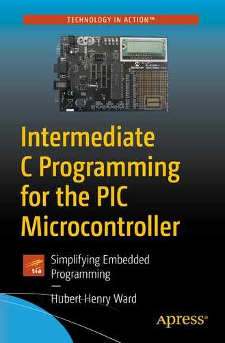
Simulation of the program
If Bit6 of the INTCON register was set to a logic 0, explain what would change and why it would change.
Explain how you could keep the logic at Bit6 of the INTCON register a logic 1, but still achieve the same result.
Using the Compare Function of the CCP Module
This function links into the use of interrupts. You will use it as the alternative method of producing a square wave, as mentioned in Chapter 4. In Chapter 4, you created the square wave using the PWM firmware of the CCP module in the PIC. This was because you were primarily creating square waves to use the PWM to set the speed of a DC motor. If all you want to do was produce a square wave, then perhaps this next method will be more efficient.
The principle behind this operation is that the compare function of the CCP compares the value of the CCPRX register with either the TMR1 or TMR3 registers. Note that these three registers can be used as simple 8-bit registers or 16-bit registers. To make them into 16-bit registers, they use two 8-bit registers cascaded together.
Briefly explain the advantage of cascading two 8-bit registers together, like this, to make a 16-bit register.
This means that each of the registers has a low byte (the CCPRXL) and a high byte (the CCPRXH), both of which can be accessed separately.
You use the x because there is CCPR1 and CCPR2. Note that by writing CCPR1 and CCPR2 you are addressing the complete 16-bit register. Writing CCPR1L means you are only addressing the low byte 8-bit register.
The CCPX can be driven high.
The CCPX can be driven low.
The CCPX can toggle; that is if, it is high, it goes low, or if it is low, it goes high.
It is the third option that can be used to create a square wave on the CCPX pin (i.e. on the CCP1 or CCP2 pin).
The Control of the Clock Sources for the Capture/Compare Mode of the CCP Modules
Bit 6 | Bit 3 | Operation |
|---|---|---|
0 | 0 | Timer 1 is the capture/compare clock source for the CCP I/O |
0 | 1 | Timer 1 is the capture/compare clock source CCP1 I/O Timer 3 is the capture/compare clock source CCP2 I/O |
1 | 0 | Timer 3 is the capture/compare clock source for the CCP I/O |
1 | 1 | Timer 3 is the capture/compare clock source for the CCP I/O |
For this program, you will set both bits to logic 0. This sets timer1 as the clock source for both the CCP I/O.
To test this concept, the following program will be created.
The Algorithm for the Compare Function
The main program will simply make an LED connected to Bit0 of PORTB flash at 0.5 seconds on and 0.5 seconds off (i.e. flash with a frequency of 1Hz).
The CCP module will compare the low byte of the CCPR1 register with the low byte of the timer1 register and, when they match, it will toggle the output of the CCP1 bit on PORTC. This will produce a square wave output on the CCP1 output. The frequency will be controlled by the value stored in the CCPR1 register.
- The frequency of square wave is controlled as follows:
The CCP1 output toggles from low to high when the value in the timer1 register equals the value stored in the CCPR1 register. At the same time, the value in timer1 will be reset to 0.
The CCP1 output will then toggle from high to low when the value in timer1 next equals the value in the CCPR1 register.
The process will repeat and the CCP1 output will toggle from low to high when the timer1 equals the CCPR1 register.
This means the square wave will have a 50/50 duty cycle and the periodic time will be twice the time taken for the value in the timer1 register to equal the value in the CCPR1 register.
To appreciate how long it will take for this to happen, you have to understand the setting of the timer1 control register T1CON.
This will be loaded with the value 0b00110001 in line 30 of the program. This makes the timer1 register an 8-bit register with a divide rate of 8. (I made it an 8-bit register simply because my PROTEUS only supports 8-bit registers.)
Knowing that the clock runs at a quarter of the oscillator and the oscillator was set to 8Mhz in the PICSetup.h header file, the clock will run at 2Mhz.
As you are using a divide rate of 8, then timer1 will count at a frequency of 250khz (i.e. 2,000,000 divided by 8).
This means one count will take 4μs as this is the periodic time for a frequency of 250kHz.
You will load the CCPR1 register with 250 and so the mark time and the space time will be 250 x 4μs = 1ms. This means that the periodic time for the square wave will be 2ms, which gives a frequency of 500Hz.
The production of this 500Hz square wave is all done with the use of the CCP1 interrupt. This interrupt is triggered when the value in the CCPR1 register is matched by the value in the timer1 or timer3 register. You are using the timer1 register. This means you need to enable the CCP1 interrupt.
The CCP1 Interrupt Program
The Analysis Of Listing 6-2
This line checks to see if the value in the TMR1L register is equal to or greater than the value on the CCPR1L register. If it is, then reset the value in the timer1 register back to 0.
The important thing to notice about this is that you are only using the low byte of the timer1 and the CCPR1 registers, hence the reference to TMR1L and CCPR1L. Also, you know the two registers will be equal to each other because that occurrence has caused the interrupt in the first place. However, you cannot ask if the two registers are equal, or use
if (TMR1L = CCPR1L) TMR1L = 0;
This is because by the time the micro gets to this instruction, the value in timer1 will be greater than the value in the CCPR1L register.
One last thing I should mention is that you have no need to ask this question at all, because the match must have happened already since the interrupt has occurred. This means you could replace this instruction with TMR1L = 0; and not use the if statement.
This is the closing curly bracket of the ISR.
Lines 15 to 22 create your variable delay subroutine from before.
This is a new instruction. What it does is perform a logical EXOR operation with Bit0 of PORTB and the logic value 1. The ^ symbol simply stands for the EXOR logic instruction.
The Truth Table for the EXOR Function
B | A | F |
|---|---|---|
0 | 0 | 0 |
0 | 1 | 1 |
1 | 0 | 1 |
1 | 1 | 0 |
This shows that the output F will be a logic 1 if A OR B are a logic 1. When the logic in both inputs are the same, the output F will be a logic 0. This is really a True OR function, as the output F will only be a logic 1 when either input A OR input B is a logic 1. The OR gate sets the output F to a logic 1 if A OR B is a logic 1, but also if A AND B are a logic 1. This is why the OR gate is sometimes called, or should be called, the inclusive OR since it includes the AND function. Note that EXOR stands for exclusive OR since it excludes the AND function.
What this means is that if Bit0 of PORTB is a logic 0, then when you EXOR it with a logic 1, the results is that bit0 goes to a logic 1. However, the next time you EXOR it with a logic 1, the two would be the same and Bit0 of PORTB is forced back to a logic 0.
This simply calls a 0.5 second delay between each EXOR operation.
These two instructions make the LED at Bit0 of PORTB oscillate on and off at a frequency of 1 Hz.

The square wave using the compare function of the CCP module
Using Priority Enabled Interrupts
Since the PIC can handle a large number of interrupts in one program, there may be a time when an interrupt is more important than the one that is running at present. In this case, the more important interrupt should be able to safely interrupt the current one and make the micro carry out its instructions of the ISR and then return to complete the instructions of the interrupt it overrode.
To enable this to happen, you can give interrupts a level of priority so that the PIC can say one interrupt is more important than another interrupt. With the PIC 18F4525, there are only two levels of priority: low priority and high priority. Other PICs may offer more levels of priority; indeed, the 32-bit PICs offer up to seven levels of priority.
The high-level interrupt can override a low-priority one but a low-priority interrupt cannot override a high-priority interrupt. Also, an interrupt cannot override an interrupt of the same priority. The PIC 18f4525 only has two levels of priority, which is not very extensive, but it is an attempt to provide a useful application.
To show you what you can do with the priority interrupts with the PIC 18F4525 I have written a program that incorporates a high and low level interrupt. It will use INT1 as the low priority interrupt and INT2 as the high priority interrupt. To keep the analysis simple, these will be the only interrupts used.
The Algorithm for the High/Low Priority Program
The first change is to set the IPEN bit, which is Bit7 of the RCON register. This is needed to enable the priority function of the interrupts.
Next, you need to set the priority level for the two interrupts you are going to use.
INT1 can be set to either low or high priority. This is controlled by the INT1IP (interrupt1 interrupt priority bit), which is Bit6 of the INTCON3 register. To set this to low priority, you simply set this bit to a logic 0.
INT2 can be set to either low or high priority. This is controlled by the INT2IP (interrupt2 interrupt priority bit), which is Bit7 of the INTCON3 register. To set the INT2 to high priority, this bit must be set to a logic 1.
You must enable these two interrupts and their interrupt enable pins are Bit4 for INT2 and Bit3 for INT1 of the INTCON3 register. These two bits must be set to a logic 1 to enable the two external interrupts.
This means that the data to be written to the INTCON3 register is 0b10011000. This is done using the instruction INTCON3 = 0b10011000;.
You also need to enable the global high priority interrupts, which means Bit7 of the INTCON register must be set to a logic 1.
As the IPEN bit is set to a logic 1 and you are using low-priority interrupts, you need to set Bit6 of the INTCON register, since now Bit6 is used to enable all low-priority interrupts.
This means that the data to be written to the INTCON register is 0b11000000. This is done using the instruction INTCON = 0b11000000;.
Since you are using both high- and low-priority interrupts, you need to write two interrupt service routines, one for the high priority and one for the low priority. Note that the PIC has two vector locations in the program memory area; this is shown in Figure 6-4. The high priority vector is at address 0008h and the low priority vector address is at 0018h. It is at these two addresses where the housekeeping software of the PIC stores the address of the two respective interrupt service routines. When the PIC is called to go to the ISR, it goes to the respective vector address to find the address it needs to load into the program counter for the respective ISR. These vector locations are shown in the program memory map in Figure 6-4.

The user memory map for the PIC18f4525
Again, because of the uncertainty of the keyword interrupt, you should use the XC8 v1.35 compiler software when creating the project.
I downloaded this program to my prototype board and it worked perfectly.
The Code For the High/Low Priority Interrupts
Analysis of Listing 6-3
Lines 1 to 9 are just some normal comments about the program. Lines 10 and 11 are the two major include files. I did not include the PICSetUp.h header file because I want to remind you about some important control registers.
This makes the PIC wait until the switch connected to Bit4 of PORTB goes to a logic 1. This is because while the logic on the bit is a logic 0, signified by the ! (or NOT) symbol, the PIC will do nothing.
The opening curly bracket of the main loop.
This sets Bits 3, 2, 1, and 0 to a logic 1. This then makes all 13 bits that could be analog set to digital.
This just sets bit 0 of PORTC to a logic 1.
The remaining lines of the program just set up a forever loop with Bit0 of PORTD simply flashing one second on and one second off.
Explanation of How the High/Low Priority Program Works
The main program just makes Bit0 of PORTD flash on and off. If you momentarily press the switch on Bit1 of PORTB, you will initiate the INT1 interrupt. The PIC will get the address of the low-priority ISR from the low-priority vector at location 0018h. The PIC will then go to the low-priority ISR where it will carry out the instruction to reset the INT1 interrupt flag. If it didn’t do this, the PIC would continually think the INT1 interrupt had been caused and you could not move on. This is because, unlike the situation with non-priority interrupts, the PIC does not turn off all interrupts by temporarily setting Bit7 of the INTCON register to a logic 0 whenever an interrupt is initiated. This is because with priority interrupts you need all interrupts to be still enabled so that a higher priority interrupt can override the current interrupt.
The PIC then carries out the instruction PORTC = 0X2C;. Bit0 of PORTD will stop flashing as long as the PIC is carrying out the instructions of the ISR for INT1. This is because the PIC will not be looking at the instructions in the main program.
The PIC then waits for the user to momentarily press the switch on Bit5 of PORTB. This is to give you time to activate INT2. If you do activate INT2, then, because it has a higher priority than INT1, the PIC will break out of the low-priority ISR and go to the high-priority ISR.
The first thing it does after resetting the INT2 interrupt flag, neglecting the test to see if it was the INT2 interrupt, is to carry out the instruction PORTC = 0X0F. This will overwrite what was in PORTC. This is so that you know the PIC is now running the high-priority ISR.
Now the PIC waits for you to momentarily press the switch on Bit4 of PORTB. This is to give you time to try to activate the INT1 interrupt. However, because INT1 is a low-priority interrupt, it cannot override the INT2 ISR.
Now when you send Bit4 momentarily to a logic 1, the PIC can move onto the next instruction in the high-priority ISR. This is where it loads PORTC with the value 0. This will set all of the bits on PORTC to a logic 0.
Now, if the INT2 had interrupted the low-priority interrupt INT1, the PIC would have gone back to the instruction on line 37 of if (!PORTBbits.RB5); where it is waiting for you to momentarily press the switch connected to Bit5. You should be able to appreciate that the PIC has gone back to this instruction because Bit0 of PORTD is still not flashing. If you now momentarily press the switch on Bit5 of PORTB, you should see Bit0 of PORTD start to flash again.

The high and low priority interrupts
Summary
In this chapter, you learned what interrupts within the microcontroller are and why you have them. You studied how to set them up and use them. You learned the difference between high and low priority interrupts and how to set up the priority interrupts and use them.
You had a brief look at the fetch and execute cycle that all micros must go through when carrying out an instruction. You also looked at the important special function register called the program counter.
I hope you have found this chapter useful. In the next chapter, you will look at the capture aspect of the CCP module and the use of the EEPROM in the PIC.