Light-sensitive circuits
The previous four chapters have dealt with the theory and applications of light-generating and light-reflecting devices such as LEDs and LCDs. The present chapter concentrates on the operating principles and applications of light-sensitive devices such as LDRs and photodiodes, etc.
LDR basics
Electronic optosensors are devices that alter their electrical characteristics in the presence of visible or invisible light. The best known devices of these types are the LDR (light dependent resistor), the photodiode, the phototransistor, and the PIR (passive infra-red) detector.
LDR operation relies on the fact that the conductive resistance of a film of cadmium sulphide (CdS) varies with the intensity of light falling on the face of the film. This resistance is very high under dark conditions and low under bright conditions. Figure 6.1 shows the LDR’s circuit symbol and basic construction, which consists of a pair of metal film contacts separated by a snake-like track of light-sensitive cadmium sulphide film, which is designed to provide the maximum possible contact area with the two metal films. The structure is housed in a clear plastic or resin case, to provide free access to external light.

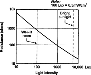
Practical LDRs are available in a variety of sizes and package styles, the most popular size having a face diameter of roughly 10mm. Figure 6.2 shows the typical characteristic curve of such a device, which has a resistance of about 900R at a light intensity of 100 Lux (typical of a well lit room) or about 30R at an intensity of 8000 Lux (typical of bright sunlight). The resistance rises to several megohms under dark conditions.
LDRs are sensitive, inexpensive, and readily available devices with power and voltage handling capabilities similar to those of conventional resistors. Their only significant defect is that they are fairly slow acting, taking tens or hundreds of milliseconds to respond to sudden changes in light level. Useful LDR applications include light- and dark-activated switches and alarms, light-beam alarms, and reflective smoke alarms, etc. Figures 6.3 to 6.22 show some practical applications of the device; each of these circuits will work with virtually any LDR with a face diameter in the range 3mm to 12mm.


LDR light-switches
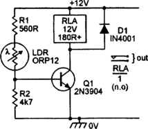
Figures 6.3 to 6.8 show some practical relay-output light-activated switch circuits based on the LDR. Figure 6.3 shows a simple non-latching circuit, designed to activate when light enters a normally dark area such as the inside of a safe or cabinet, etc.
Here, R1–LDR and R2 form a potential divider that controls the base-bias of Q1. Under dark conditions the LDR resistance is very high, so negligible base-bias is applied to Q1, and Q1 and RLA are off. When a significant amount of light falls on the LDR face the LDR resistance falls to a fairly low value and base-bias is applied to Q1, which thus turns on and activates the RLA/1 relay contacts, which can be used to control external circuitry. The relay can be any 12V type with a coil resistance of 180R or greater.
The simple Figure 6.3 circuit has a fairly low sensitivity, and has no facility for sensitivity adjustment. Figure 6.4 shows how these deficiencies can be overcome by using a super-alpha-connected pair of transistors in place of Q1, and by using sensitivity control RV1 in place of R2; this circuit can be activated by LDR resistances as high as 200k (i.e. by exposing the LDR to very small light levels), and draws a standby current of only a few microamps under ‘dark’ conditions. The diagram also shows how the circuit can be made to give a self-latching action via relay contacts RLA/2; normally-closed push-button switch S1 enables the circuit to be reset (unlatched) when required.
Figure 6.5 shows how a LDR can be used to make a simple dark-activated relay switch that turns RLA on when the light level falls below a value preset via RV1. Here, R1 and LDR form a potential divider that generates an output voltage that rises as the light level falls. This voltage is buffered by emitter-follower Q1 and used to control relay RLA via common-emitter amplifier Q2 and current-limiting resistor R3.
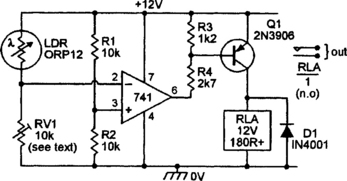
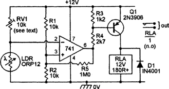
The light trigger points of the Figure 6.3 to 6.5 circuits are susceptible to variations in circuit supply voltage and ambient temperature. Figure 6.6 shows a very sensitive precision light-activated circuit that is not influenced by such variations. In this case, LDR–RV1 and R1–R2 are connected in the form of a Wheatstone bridge, and the op-amp and Q1–RLA act as a highly sensitive balance-detecting switch. The bridge balance point is quite independent of variations in supply voltage and temperature, and is influenced only by variations in the relative values of the bridge components.
In Figure 6.6, the LDR and RV1 form one arm of the bridge, and R1–R2 form the other arm. These arms act as potential dividers, with the R1–R2 arm applying a fixed half-supply voltage to the non-inverting input of the op-amp, and with the LDR–RV1 divider applying a light-dependent variable voltage to the inverting terminal of the op-amp.
In use, RV1 is adjusted so that the LDR–RV1 voltage rises slightly above that of R1–R2 as the light intensity rises to the desired trigger level, and under this condition the op-amp output switches to negative saturation and thus drives the relay on via Q1 and biasing resistors R3–R4. When the light intensity falls below this level, the op-amp output switches to positive saturation, and under this condition Q1 and the relay are off.
The Figure 6.6 circuit is very sensitive and can detect light-level changes too small to be seen by the human eye. The circuit can be modified to act as a precision dark-activated switch by either transposing the inverting and non-inverting input terminals of the op-amp, or by transposing RV1 and the LDR. Figure 6.7 shows a circuit using the latter option.
Figure 6.7 also shows how a small amount of hysteresis can be added to the circuit via feedback resistor R5, so that the relay turns on when the light level falls to a particular value, but does not turn off again until the light intensity rises a substantial amount above this value. The magnitude of hysteresis is inversely proportional to the R5 value, being zero when R5 is open-circuit.
A precision combined light/dark switch, which activates a single relay if the light intensity rises above one pre-set value or falls below another preset value, can easily be made by combining an op-amp light switch and an op-amp dark switch in the manner shown in Figure 6.8.
To set up the Figure 6.8 circuit, first trim RV1 so that approximately half-supply volts appear on the LDR–RV1 junction when the LDR is illuminated at the mean or normal intensity level. RV2 can then be pre-set so that RLA turns on when the light intensity falls to the desired dark level, and RV3 can be adjusted so that RLA activates at the desired brightness level.
Note in Figures 6.6 to 6.8 that the adjusted RV1 value should equal the LDR resistance value at the normal light level of each circuit.
Bell-output LDR alarms
The Figure 6.3 to 6.8 light-activated LDR circuits all have relay outputs that can be used to control virtually any type of external circuitry. In some light-activated applications, however, circuits are required to act as audible-output alarms, with a bell or siren-sound output, and this type of action can be obtained without the use of relays. Figures 6.9 to 6.11 show three practical ‘alarm bell output’ circuits of this type.
The Figure 6.9 to 6.11 circuits are each designed to give a direct output to an alarm bell, which must be of the self-interrupting type and must consume an operating current of less than 2A. The supply voltage of each circuit should be 1.5V to 2V greater than the nominal operating value of the bell.
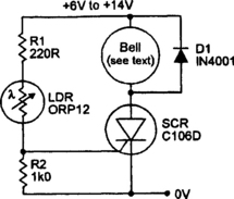
Figure 6.9 shows the circuit of a simple light-activated alarm; the operating theory is fairly simple. The R1–LDR and R2 form a potential divider: under dark conditions the LDR resistance is high, so the LDR–R2 junction voltage is too small to activate the gate of the SCR (silicon controlled rectifier), but under bright conditions the LDR resistance is low, so gate bias is applied to the SCR, which turns on and activates the alarm bell.
Note in the above circuit that, although the SCR is a self-latching device, the fact that the bell is of the self-interrupting type ensures that the SCR automatically unlatches repeatedly as the bell operates (and the SCR anode current falls to zero in each self-interrupt phase). Consequently, the alarm bell automatically turns off again when the light level falls back below the trip level.
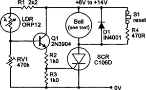
The Figure 6.9 circuit has a fairly low sensitivity and has no facility for sensitivity adjustment. Figure 6.10 shows how these weaknesses can be overcome by using RV1 in place of R2 and by using Q1 as a buffer between the LDR and the SCR gate. This diagram also shows how the circuit can be made self-latching by wiring R4 across the bell so that the SCR anode current does not fall to zero as the bell self-interrupts. Switch S1 enables the circuit to be reset (unlatched) when required.
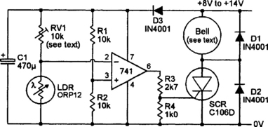
Figure 6.11 shows how to make a precision light-activated alarm with a SCR-driven alarm bell output by using a Wheatstone bridge (LDR–RV1–R1–R2) and an op-amp balance detector to give the precision action (as described in the basic Figure 6.6 circuit). This circuit can be converted into a dark-activated alarm by simply transposing RV1 and the LDR. Hysteresis can also be added, if required.
Siren-output LDR alarms
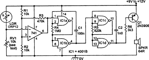
Figures 6.12 to 6.17 show ways of using CMOS 4001B quad 2-input NOR gate ICs as the basis of various light-activated ‘siren-sound’ alarms that generate audible outputs in loudspeakers. The Figure 6.12 circuit is that of a light-activated alarm that generates a low-power (up to 520mW) 800Hz pulsed-tone signal in the speaker when the light input exceeds a pre-set threshold value. Here, IC1c and IC1d are wired as an 800Hz astable multivibrator that can feed tone signals into the speaker via Q1 and is gated on only when the output of IC1b is low, and IC1a–IC1b are wired as a 6Hz astable that is gated on only when its pin-1 gate terminal (which is coupled to the LDR–RV1 potential divider) is pulled low.
The action of the Figure 6.12 circuit is as follows. Under dark conditions the LDR–RV1 junction voltage is high, so both astables are disabled and no signal is generated in the speaker. Under ‘light’ conditions the LDR–RV1 junction voltage is low, so the 6Hz astable is activated and in turn gates the 800Hz astable on and off at a 6Hz rate, thereby generating a pulsed-tone signal in the speaker via Q1.
The precise switching or gate point of the 4001B IC is determined by the threshold voltage value of the IC, and this is a percentage value of the supply voltage: the value is nominally 50%, but may vary from 30% to 70% between individual ICs. In practice, the switching point of each individual 4001B IC is very stable, and the Figure 6.12 circuit gives very sensitive ‘light’-activated alarm triggering.
Figure 6.13 shows the circuit of a self-latching light-activated alarm with a 800Hz monotone output. In this case IC1c–IC1d are again wired as a gated 800Hz astable, but IC1a–IC1b are wired as a bistable multivibrator with an output that (under dark conditions) is normally high, thus gating the 800Hz astable off. Under bright conditions, however, the LDR–RV1 junction goes high and latches the bistable into its alternative ‘output low’ state, thereby gating the 800Hz astable on and generating the monotone alarm signal; once latched, the circuit remains in this ‘on’ state until dark conditions return and the bistable is simultaneously reset via S1.
Note that the light/dark operation of the Figure 6.12 and 6.13 circuits can be reversed by simply transposing the LDR–RV1 positions. The sensitivity levels of these two basic circuits are adequate for most practical purposes, but can, if required, be boosted (and the trigger-level stability increased), by interposing an op-amp voltage comparator (of the basic Figure 6.6 or 6.7 type) between the LDR–RV1 light-sensitive potential divider and the gate terminal of the CMOS waveform generator, as shown in the Figure 6.14 circuit; resistor R3 controls the hysteresis of the circuit, and can be removed if the hysteresis is not needed.
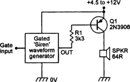
The basic Figure 6.12 to 6.14 circuits generate fairly modest values of acoustic output power, with the power input to the 64 ohm loudspeaker reaching a maximum value of 520mW when using a 12V supply. If desired, the input power to the loudspeaker can be boosted to well over a dozen watts by using more complex output-driving circuitry, as shown in Figures 6.15 to 6.17. Note in all these circuits that maximum acoustic output powers can be obtained by using cheap horn-type loudspeakers, which typically have electro-acoustic power conversion efficiencies that are twenty to forty times greater than normal hi-fi speakers.
Figure 6.15 shows the type of output stage that is used in the basic Figure 6.12 to 6.14 circuits. Thus, when the siren waveform generator is gated off its output is high and Q1 is thus cut off, but when the generator is gated on its output drives Q1 on and off and causes it to feed power to the 64R speaker. The output power depends on the supply rail voltage, and has a value of about 520mW at 12V, or 120mW at 6V, when feeding a 64R speaker load. Note that, since Q1 is used as a simple power switch in this application, very little power is lost across the 2N3906 transistor, but its current rating (200mA maximum) may be exceeded if the circuit is used with a supply value greater than 12V.
Figure 6.16 shows how the basic Figure 6.15 circuit can be modified so that it can feed a maximum of 6.6 watts of audio power into an 8R0 speaker load, or 3.3 watts into a 16R load. Here, both transistors are cut off when the waveform generator is gated off, but are switched on and off in sympathy with the siren waveform when the generator is gated on. Note in this circuit that the positive power supply rail is fed directly to the output driver, but is fed to the waveform generator via decoupling network R1–C1, that voltage divider R2–R3 ensures that the output stages are not driven on until the generator’s output voltage falls at least 1.9V below the supply rail value, and that diode D1 is used to damp the speaker’s back-e.m.f. when driver Q2 switches off.
Finally, the Figure 6.17 driver circuit can pump a maximum of 13.2 watts into a 4R0 speaker load when powered from a 15V supply. Here, all three transistors are cut off when the waveform generator is cut off, but are switched on and off in sympathy with the siren waveform when the generator is gated on.
Miscellaneous LDR circuits
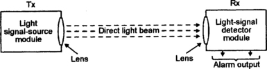
One of the best-known types of LDR application is in light-beam alarms or switches. A light-beam alarm system consists of a focused light-beam transmitter (Tx) and a focused light-beam receiver (Rx), and may be configured to give either a direct-light-beam or a reflected-light-beam type of optical contact operation. Figure 6.18 shows the basic elements of a direct-light-beam type of alarm system, in which the sharply focused Tx light-beam is aimed directly at the light-sensitive input point of the Rx unit, which (usually) is designed to activate an external alarm or safety mechanism if a person, object, or piece of machinery enters the light-beam and breaks the optical contact between the Tx and Rx.
Figure 6.19 shows a very simple example of a lamp-and-LDR direct-light-beam system that activates an alarm-bell if the beam is interrupted. The beam is generated via an ordinary electric lamp and a lens, and is focused (via a ‘collector’ lens) on to the face of an LDR in the remote Rx unit, which operates as a dark-activated alarm. Normally, the LDR face is illuminated by the light-beam, so the LDR has a low resistance and very little voltage thus appears on the RV1–LDR junction, so the SCR and bell are off. When the light-beam is broken, however, the LDR resistance goes high and enough voltage appears on the RV1–LDR junction to trigger the SCR, which drives the alarm bell on; R3 is used to self-latch the alarm.
Figure 6.20 shows the basic elements of a reflected-light-beam type of alarm system, in which the Tx light-beam and Rx lens are optically screened from each other but are both aimed outwards towards a specific point, so that an optical link can be set up by a reflective object (such as metallic paint or smoke or fog particles) placed at that point. This type of system is usually designed to activate an alarm when the presence of such an object is detected, but can also be configured to give the reverse action, so that the alarm activates if a reflective object is illegally removed.
Units of the Figure 6.20 type were once widely used in conjunction with reflection-type fog and smoke detector units; Figure 6.21 shows a sectional view of a smoke detector unit of this type. Here, the lamp and LDR are mounted in an open ended but light-excluding box, in which an internal screen prevents the lamp-light from falling directly on the LDR face. The lamp is a source of both light and heat, and the heat causes convection currents of air to be drawn in from the bottom of the box and to be expelled through the top. The inside of the box is painted matt black; its construction lets air pass through the box but excludes external light.
Thus, if the convected air currents are smoke free, no light falls on the LDR face, and the LDR presents a high resistance. If the air currents do contain smoke, however, the smoke particles cause the light of the lamp to reflect on to the LDR face and so cause a large and easily detectable decrease in the LDR resistance. Figure 6.22 shows a reflection-type smoke alarm circuit that can be used with this detector; the circuit acts in the same way as the improved Figure 6.10 light-activated alarm circuit.
Simple lamp-and-LDR light-beam alarms of the types described in this section have several obvious disadvantages in most modern security-alarm applications. Their light-beams are, for example, clearly visible to an intruder, the transmitter’s filament lamp is unreliable, and the systems are (because the transmitter’s filament lamp wastes a lot of power) very inefficient. In practice, virtually all modern light-beam security systems operate in the invisible infra-red (rather than visible light) range, use one or more pulse-driven IR LEDs to generate the transmitter’s ‘light-beam’, and use matching IR photodiodes or phototransistors to detect the beam at the receiver end of the system. A number of practical circuits of these types are presented in Chapter 11 of this book.
Photodiodes
Cadmium sulphide (CdS) LDRs are sensitive but slow-acting light sensors. Generally, they are ideal for use in slow-acting direct-coupled light-level sensing applications, but are quite unsuitable for use as optical sensors in medium- to high-speed applications. The ideal optical sensors for use in the latter types of application are the silicon photodiode and the silicon phototransistor.
In its very crudest form, a photodiode is a normal silicon diode minus its opaque (light-excluding) covering. If a normal silicon diode is connected in the reverse-biased circuit of Figure 6.23, negligible current flows through the diode and zero voltage is developed across R1. If the diode’s opaque covering is now removed (so that the diode’s semiconductor junction is revealed) and the junction is then exposed to visible light in the same circuit, the diode will pass a significant reverse current and thus generate an output voltage across R1. The magnitude of the reverse current and the output voltage is directly proportional to the intensity of the light source, and the diode is thus truly photosensitive.
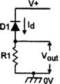
All silicon junctions are photosensitive, and a basic photodiode can – for most practical purposes – be regarded as a normal diode housed in a case that lets external light easily reach its photosensitive semiconductor junction. Figure 6.24(a) shows the standard photodiode symbol. In use, the photodiode is reverse biased and the output voltage is taken from across a series-connected load resistor; this resistor can be connected between the diode and ground, as in Figure 6.24(b), or between the diode and the positive supply line, as in Figure 6.24(c).

Figure 6.24 Photodiode symbol (a) and alternative ways ((b) and (c)) of using a photodiode as a light-to-voltage converter
In reality, the physical form of a normal silicon diode’s pn junction is such that the device exhibits fairly low optical sensitivity; all practical photodiodes use special types of junction design to maximize their effective photosensitivity. Most photodiodes come in one or other of two basic types, being either ‘simple’ photodiodes or PIN photodiodes. Figure 6.25 illustrates some basic points on these subjects.
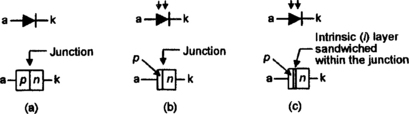
Figure 6.25 Symbol and basic construction of (a) a normal silicon junction diode, (b) a simple photodiode, and (c) a PIN photodiode
Normal silicon junction diodes use the basic form of construction shown (in symbolic form) in Figure 6.25(a), in which the device’s p- and n-type materials are moderately thick (and thus fairly opaque) and are effectively fused directly together to form the device’s junction; the relatively high opacity of the pn junction’s materials gives the junction fairly poor photosensitivity. In a simple photodiode, the photosensitivity is greatly increased by using a very thin (and thus highly translucent) slice of material on the p-type side of the junction, as shown in Figure 6.25(b); external light can be applied, via a built-in lens or window, to the optosensitive pn junction via this thin slice of p-type material.
Simple Figure 6.25(b)-type photodiodes have minimum on/off switching times of about 1μs, and can thus be used at maximum pulsed or switched operating frequencies of about 300kHz. The prime cause of this relatively long switching time is the high capacitance that occurs at the device’s junction, between the p- and n–type materials. This problem is greatly reduced in PIN photodiodes, in which a very thin slice of intrinsic (‘I’) or ‘undoped’ silicon material is interposed at the junction between the p- and n–type materials, as shown in Figure 6.25(c), thus greatly reducing the p-to-n junction’s capacitance value.
Modern PIN-type photodiodes have typical minimum on/off switching times of about 10ns, and can thus be used at maximum switched-mode operating frequencies of about 30MHz, which is adequate for the vast majority of practical optoelectronic applications (in cases where even higher switching frequency optical sensing is required, special ultra-high-frequency avalanche-type photodiodes can be used).
Photodiodes can be designed to respond to either visible light or to IR light. The human eye has the type of spectral response curve shown in curve ‘a’ in Figure 6.26. It has a maximum sensitivity to the colour green, which has a wavelength of about 550nm, but has a relatively low sensitivity to the colour violet (400nm) at one end of the spectrum and to dark red (700nm) at the other. General-purpose visible-light photodiodes have typical spectral response characteristics like those shown in curve ‘b’ in Figure 6.26, and infra-red (IR) types have the type of response shown in curve ‘c‘.

Phototransistors
Ordinary silicon transistors are made from an npn or pnp sandwich, and thus inherently contain a pair of photosensitive junctions. Some types are available in phototransistor form, and use the standard symbol shown in Figure 6.27(a). Figures 6.27(b) to 6.27(d) show three basic ways of using a phototransistor; in each case the base–collector junction is effectively reverse biased and thus acts as a photodiode. In (b) the base is grounded, and the transistor acts as a simple photodiode. In (c) and (d) the base terminal is open-circuit and the photogenerated currents effectively feed directly into the base and, by normal transistor action, generate a greatly amplified collector-to-emitter current that produces an output voltage across series resistor R1.
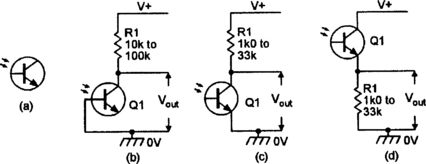
The sensitivity of a phototransistor is typically one hundred times greater than that of a photodiode, but its useful maximum operating frequency (usually a few hundred kilohertz) is proportionally lower than that of a photodiode. Most phototransistors are manufactured in 2-pin form, with only the device’s collector and emitter made externally available; 3-pin types can be used in any of the basic configurations shown in Figure 6.27. Some phototransistors are made in very-high-gain Darlington form.
The sensitivity (and operating speed) of a 3-pin phototransistor can be made variable by wiring a variable resistor between its base and emitter, as shown in Figure 6.28; with RV1 open circuit, phototransistor operation is obtained; with RV1 short circuit, photodiode operation occurs.

Note in the Figure 6.24, 6.27, and 6.28 photodiode and phototransistor circuits that, in practice, the R1 load value is usually chosen on a compromise basis, since the circuit sensitivity increases but the useful operating bandwidth decreases as the R1 value is increased. Also, the R1 value must, in many applications, be chosen to bring the photosensitive device into its linear operating region.
IR pre-amp circuits
Photodiodes or phototransistors are often used as the sensing elements at the receiver end of light-beam alarms, remote-control, or fibre optic cable systems. In such applications, the signal reaching the photosensor may vary considerably in strength, and the sensor may be subjected to a great deal of noise in the form of unwanted visible or IR light signals, etc. To help minimize these problems, the systems are usually operated in the IR range, and the optosensor output is passed to processing circuitry via a low-noise pre-amplifier with a wide dynamic operating range. Figures 6.29 and 6.30 show typical examples of such circuits, using photodiode sensors.

The Figure 6.29 circuit is designed to detect an IR optical signal that is switched at a 30kHz rate. Photodiode D1 senses the IR signal and feeds it into 30kHz tuned circuit L1–C1–C2, which is lightly damped by R1. The resulting frequency-selected low-noise output of the tuned circuit is tapped off at the C1–C2 junction and then amplified by Q1.
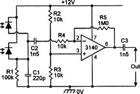
Finally, Figure 6.30 shows a 20kHz selective pre-amplifier circuit for use in an IR light-beam alarm application in which the alarm sounds when the beam is broken. Here, two IR photodiodes are wired in parallel (so that beam signals are lost only when both diode signals are cut off) and share a common 100k load resistor (R1). This resistor is shunted by C1 to reject unwanted high-frequency signals, and the R1 output signals are fed to the × 100 op-amp inverting amplifier via C2, which rejects unwanted low-frequency signals.
PIR movement-detecting systems
IR light-beam alarms are active IR units that react to an artificially generated source of IR radiation. Passive IR (PIR) alarms, on the other hand, react to naturally generated IR radiation such as the heat-generated IR energy radiated by the human body, and are widely used in modern security systems. Most PIR security systems are designed to activate an alarm or floodlight, or open a door or activate some other mechanism, when a human or other large warm-blooded animal moves about within the sensing range of a PIR detector unit, and use a pyroelectric IR detector of the type shown in Figure 6.31 as their basic IR-sensing element.
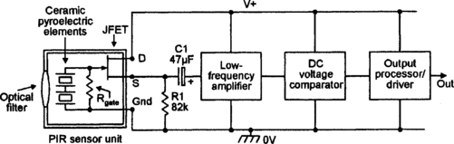
The basic Figure 6.31 pyroelectric IR detector makes use of special ceramic elements that generate electrical charges when subjected to thermal variations or uneven heating. Modern pyroelectric IR detectors such as the popular PIS201S and E600STO types incorporate two small opposite-polarity series-connected ceramic elements of this type, with their combined output buffered via a JFET source-follower, and have the IR input signals focused onto the ceramic elements by a simple filtering lens, as shown in the basic PIR detector usage circuit of Figure 6.31. It is important to note at this point that the detector’s final output voltage is proportional to the difference between the output voltages of the two ceramic elements.
The basic action of the Figure 6.31 PIR detector is such that, when a human body is within the visual field of the pyroelectric elements, part of that body’s radiated IR energy falls on the surfaces of the elements and is converted into a small but detectable variation in surface temperature and corresponding variation in the output voltage of each element. If the human body (or other source of IR radiation) is stationary in front of the detector’s lens under this condition, the two elements generate identical output voltages and the unit’s final ‘difference’ output is thus zero, but if the body is moving while in front of the lens the two elements generate different output voltages and the unit produces a varying output voltage.
Thus, when the PIR unit is wired as shown in the Figure 6.31 basic usage circuit, this movement-inspired voltage variation is made externally available via the buffering JFET and dc-blocking capacitor C1 and can, when suitably amplified and filtered, be used to activate an alarm or other mechanism when a human body movement is detected. In practice, pyroelectric IR detectors of the simple type just described have, because of the small size (usually about 20mm2) and simple design of the detector’s IR-gathering lens, maximum useful detection ranges of roughly one metre. In modern commercial PIR movement detecting security units, however, this range is usually extended to at least ten metres with the aid of a large (about 2000mm2) multi-faceted external IR-gathering/focusing plastic lens, which splits the visual field into a number of parallel strips and focuses them onto the two sensing areas of the PIR unit.
Figure 6.32 shows the typical PIR sensing pattern of a commercial ‘intrusion detector’ unit designed to protect a normal-sized room in domestic-type applications. In this example the unit is mounted on a wall at a height of seven feet and is aimed downwards at a shallow angle, and the multi-faceted plastic lens splits the visual field into a large number of vertical and horizontal segments. Any person moving through a single segment will activate a single trigger signal within the PIR sensor; a person moving through the entire visual field will thus produce numerous triggering signals, but a stationary IR source will produce no signals. Most intrusion detectors of this type incorporate ‘event counting’ circuitry that will only generate an alarm-activating output if three or more trigger signals are detected within a few seconds, thus minimizing the chances of a false alarm due to sudden changes in temperature caused by the auto-activation of time-switched security lights, etc.
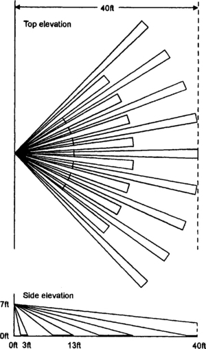
Figure 6.32 Typical PIR sensing pattern of a commercial ‘intrusion detector’ unit designed for normal domestic-type applications
The lens-generated PIR sensor pattern shown in Figure 6.32 is the type usually used to protect single rooms in domestic burglar-alarm systems. Alternative lenses offer different ranges and coverage patterns for various special types of application; among the most important of these are the ‘pet’ type, in which the field’s vertical span is restricted to 2.5 to 6.6 feet above ground level to avoid activation by domestic pets while giving good sensitivity to normal humans, and the ‘corridor’ type, in which the field’s horizontal span is restricted to about 20 degrees to give long-distance coverage (typically about 30 metres) of narrow corridors and passageways.
Note that, because high-quality commercial PIR security units of this basic type are widely available at comparatively low cost, it is not practicable (on aesthetic and cost-effective grounds) to try to build similar units on a DIY basis.