
12.7 Counter ICs
In Sec. 12.6.5, you saw how flip-flops could be combined to make both asynchronous (ripple) and synchronous counters. In practice, using discrete flip-flops is to be avoided. Instead, use a prefabricated counter IC. These ICs cost a dollar or two and come with many additional features, like control enable inputs, parallel loading, and so on. A number of different kinds of counter ICs are available. They come in either synchronous (ripple) or asynchronous forms and are usually designed to count in binary or binary-coded decimal (BCD).
12.7.1 Asynchronous Counter (Ripple Counter) ICs
Asynchronous counters work fine for many noncritical applications, but for high-frequency applications that require precise timing, synchronous counters work better. Recall that unlike an asynchronous counter, a synchronous counter contains flip-flops that are clocked at the same time, and hence the synchronous counter does not accumulate nearly as many propagation delays as is the case with the asynchronous counter. Let's look at a few asynchronous counter ICs you will find in the electronics catalogs.
7493 4-Bit Ripple Counter with Separate MOD-2 and MOD-8 Counter Sections
The 7493's internal structure consists of four JK flip-flops connected to provide separate MOD-2 (0-to-1 counter) and MOD-8 (0-to-7 counter) sections. Both the MOD-2 and MOD-8 sections are clocked by separate clock inputs. The MOD-2 section uses Cp0 as its clock input, while the MOD-8 section uses Cp1 as its clock input. Likewise, the two sections have separate outputs: MOD-2's output is Q0, while MOD-8's outputs consist of Q1, Q2, and Q3. The MOD-2 section can be used as a divide-by-2 counter. The MOD-8 section can be used as a divide-by-2 counter (output tapped at Q1), a divide-by-4 counter (output tapped at Q2), or a divide-by-8 counter (output tapped at Q3). If you want to create a MOD-16 counter, simply join the MOD-2 and MOD-8 sections by wiring Q0 to Cp1, while using Cp0 as the single clock input.
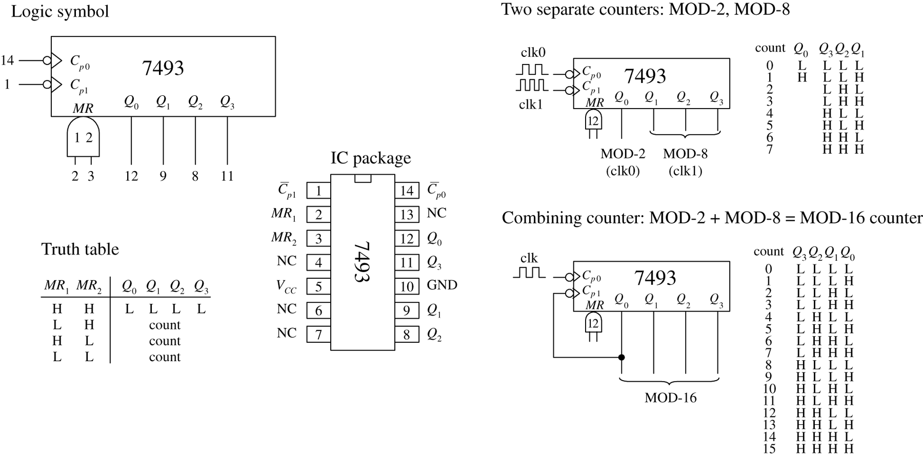
FIGURE 12.87
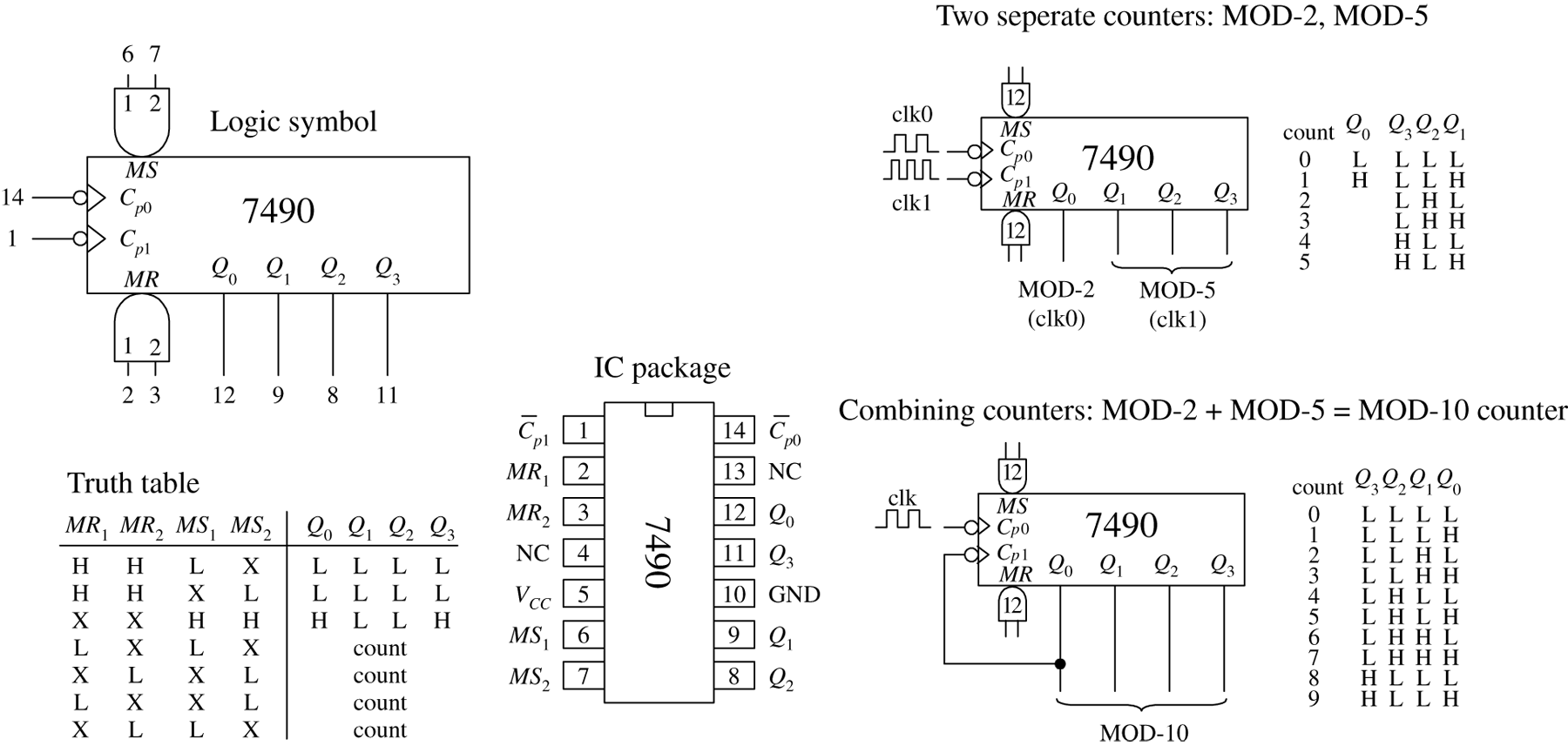
FIGURE 12.88
The MOD-2, MOD-8, or the MOD-16 counter can be cleared by making both AND-gated master reset inputs (MR1 and MR2) high. To begin a count, one or both of the master reset inputs must be made low. When the negative edge of a clock pulse arrives, the count advances one step. After the maximum count is reached (1 for MOD-2, 111 for MOD-8, or 1111 for MOD-16), the outputs jump back to zero, and a new count begins.
7490 4-Bit Ripple Counter with MOD-2 and MOD-5 Counter Sections
The 7490, like the 7493, is another 4-bit ripple counter. However, its flip-flops are internally connected to provide MOD-2 (count-to-2) and MOD-5 (count-to-5) counter sections. Again, each section uses a separate clock: Cp0 for MOD-2 and Cp1 for MOD-5. By connecting Q0 to Cp1 and using Cp0 as the single clock input, a MOD-10 counter (decade or BCD counter) can be created.
When master reset inputs MR1 and MR2 are set high, the counter's outputs are reset to 0—provided that master set inputs MS1 and MS2 are not both high (the MS inputs override the MR inputs). When MS1 and MS2 are high, the outputs are set to Q0 = 1, Q1 = 0, Q2 = 0, and Q3 = 1. In the MOD-10 configuration, this means that the counter is set to 9 (binary 1001). This master set feature comes in handy if you wish to start a count at 0000 after the first clock transition occurs (with master reset, the count starts out at 0001).
7492 Divide-by-12 Ripple Counter with MOD-2 and MOD-6 Counter Sections
The 7492 is another 4-bit ripple counter that is similar to the 7490. However, it has a MOD-2 and a MOD-6 section, with corresponding clock inputs Cp0 (MOD-2) and Cp1 (MOD-8). By joining Q0 to Cp1, you get a MOD-12 counter, where Cp0 acts as the single clock input. To clear the counter, high levels are applied to master reset inputs MR1 and MR2.
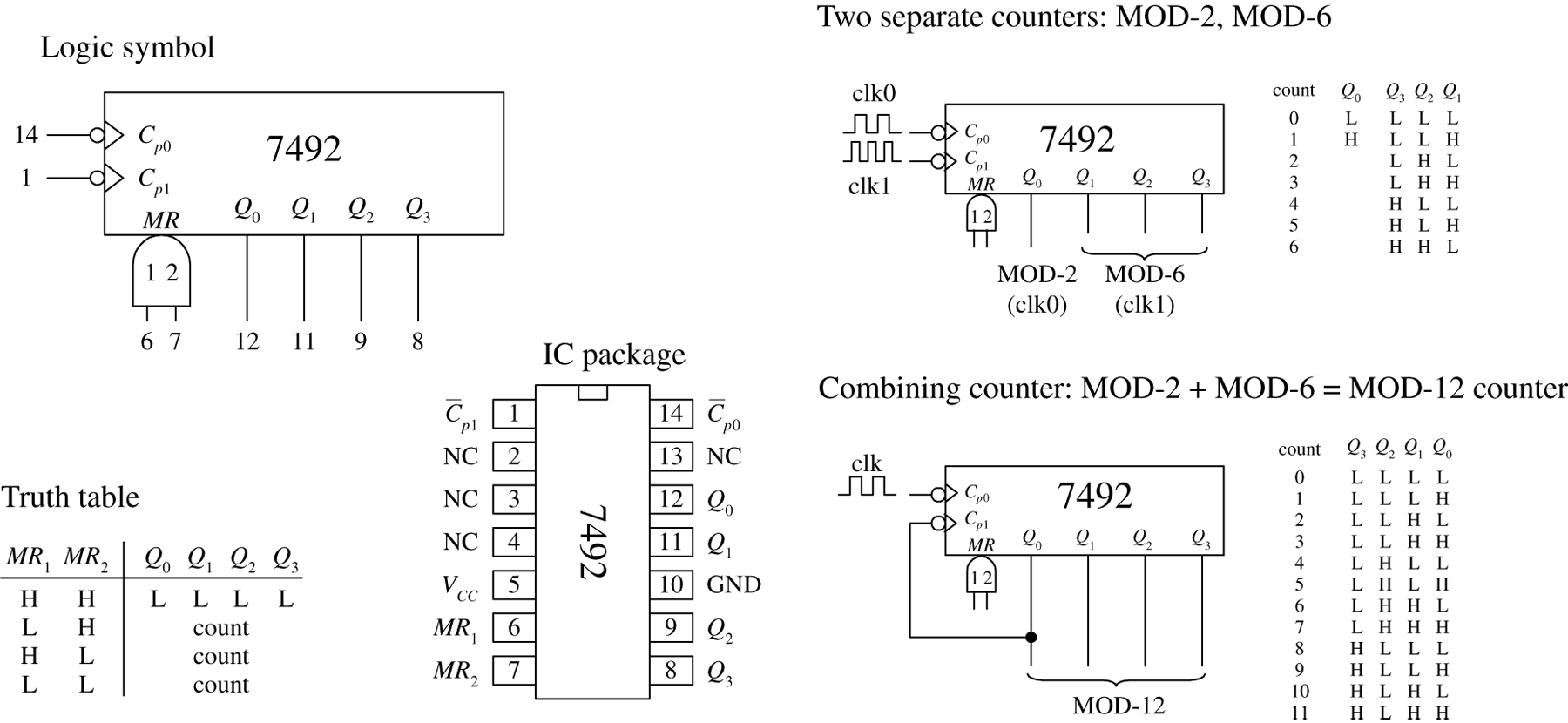
FIGURE 12.89
12.7.2 Synchronous Counter ICs
Like the asynchronous counter ICs, synchronous counter ICs come in various MOD arrangements. These devices usually come with extra goodies, such as controls for up or down counting and parallel load inputs used to preset the counter to a desired start count. Synchronous counter ICs are more popular than the asynchronous ICs, not only because of these additional features, but also because they do not have such long propagation delays as asynchronous counters. Let's take a look at a few popular IC synchronous counters.
74193 Presettable 4-Bit (MOD-16) Synchronous Up/Down Counter
The 74193 is a versatile 4-bit synchronous counter that can count up or count down and can be preset to any count desired—at least a number between 0 and 15. There are two separate clock inputs: CpU is used to count up, and CpD is used to count down. One of these clock inputs must be held high in order for the other input to count. The binary output count is taken from Q0 (20), Q1 (21), Q2 (22), and Q3 (23).
To preset the counter to any desired count, a corresponding binary number is applied to the parallel inputs D0 to D3. When the parallel load input 
![]() is pulsed low, the binary number is loaded into the counter, and the count, either up or down, will start from that number. The terminal count up (
is pulsed low, the binary number is loaded into the counter, and the count, either up or down, will start from that number. The terminal count up ( 
![]() ) and terminal count down (
) and terminal count down ( 
![]() ) outputs are normally high. The
) outputs are normally high. The ![]() output is used to indicate when the maximum count has been reached and the counter is about to recycle to the minimum count (0000)—the carry condition. Specifically, this means that
output is used to indicate when the maximum count has been reached and the counter is about to recycle to the minimum count (0000)—the carry condition. Specifically, this means that ![]() goes low when the count reaches 15 (1111) and the input clock (CpU) goes from high to low.
goes low when the count reaches 15 (1111) and the input clock (CpU) goes from high to low. ![]() remains low until CpU returns high. This low pulse at
remains low until CpU returns high. This low pulse at ![]() can be used as an input to the next high-order stage of a multistage counter. The terminal count down (
can be used as an input to the next high-order stage of a multistage counter. The terminal count down ( ![]() ) output is used to indicate that the minimum count has been reached (0000) and the counter is about to recycle to the maximum count 15 (1111)—the borrow condition. Specifically, this means that
) output is used to indicate that the minimum count has been reached (0000) and the counter is about to recycle to the maximum count 15 (1111)—the borrow condition. Specifically, this means that ![]() goes low when the down count reaches 0000 and the input clock (CpD) goes low. Figure 12.90 provides a truth table for the 74193, along with a sample load, up-count, and down-count sequence.
goes low when the down count reaches 0000 and the input clock (CpD) goes low. Figure 12.90 provides a truth table for the 74193, along with a sample load, up-count, and down-count sequence.
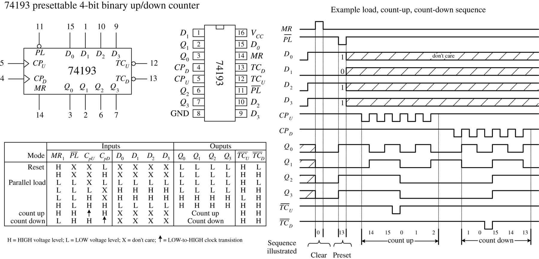
FIGURE 12.90
74192 Presettable Decade (BCD or MOD-10) Synchronous Up/Down Counter
The 74192, shown in Fig. 12.91, is essentially the same device as the 74193, except it counts up from 0 to 9 and repeats or counts down from 9 to 0 and repeats. When counting up, the terminal count up ( ![]() ) output goes low to indicate when the maximum count is reached (9 or 1001) and the CpU clock input goes from high to low.
) output goes low to indicate when the maximum count is reached (9 or 1001) and the CpU clock input goes from high to low. ![]() remains low until CpU returns high. When counting down, the terminal count down output (
remains low until CpU returns high. When counting down, the terminal count down output ( ![]() ) goes low when the minimum count is reached (0 or 0000) and the input clock CpD goes low. The truth table and example load, count-up, and count-down sequence provided in Fig. 12.91 explain how the 74192 works in greater detail.
) goes low when the minimum count is reached (0 or 0000) and the input clock CpD goes low. The truth table and example load, count-up, and count-down sequence provided in Fig. 12.91 explain how the 74192 works in greater detail.
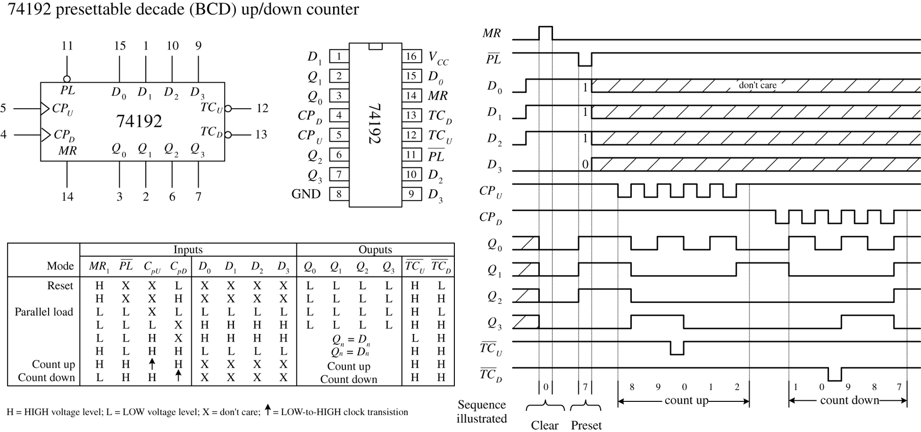
FIGURE 12.91
74190 Presettable Decade (BCD or MOD-10) and 74191 Presettable 4-Bit (MOD-16) Synchronous Up/Down Counters
The 74190 and the 74191 do basically the same things as the 74192 and 74193, but the input and output pins, as well as the operating modes, are a bit different. (The 74190 and the 74191 have the same pinouts and operating modes; the only difference is the maximum count.) Like the previous synchronous counters, these counters can be preset to any count by using the parallel load 
![]() operation. However, unlike the previous synchronous counters, to count up or down requires using a single input:
operation. However, unlike the previous synchronous counters, to count up or down requires using a single input: 
![]() . When
. When ![]() is set low, the counter counts up; when
is set low, the counter counts up; when ![]() is high, the counter counts down.
is high, the counter counts down.
A clock enable input ( 
![]() ) acts to enable or disable the counter. When
) acts to enable or disable the counter. When ![]() is low, the counter is enabled. When
is low, the counter is enabled. When ![]() is high, counting stops, and the current count is held fixed at the Q0 to Q3 outputs.
is high, counting stops, and the current count is held fixed at the Q0 to Q3 outputs.
Unlike the previous synchronous counters, the 74190 and the 74191 use a single terminal count output (TC) to indicate when the maximum or minimum count has occurred and the counter is about to recycle. In count-down mode, TC is normally low but goes high when the counter reaches zero (for both the 74190 and 74191). In count-up mode, TC is normally low but goes high when the counter reaches 9 (for the 74190) or reaches 15 (for the 74191).
The ripple-clock output ( 
![]() ) follows the input clock (CP) whenever TC is high. This means, for example, that in count-down mode, when the count reaches zero,
) follows the input clock (CP) whenever TC is high. This means, for example, that in count-down mode, when the count reaches zero, 
![]() will go low when CP goes low. The
will go low when CP goes low. The ![]() output can be used as a clock input to the next higher stage of a multistage counter. This, however, leads to a multistage counter that is not truly synchronous because of the small propagation delay from CP to
output can be used as a clock input to the next higher stage of a multistage counter. This, however, leads to a multistage counter that is not truly synchronous because of the small propagation delay from CP to ![]() of each counter. To make a multistage counter that is truly synchronous, you must tie each IC's clock to a common clock input line. You use the TC output to inhibit each successive stage from counting until the previous stage is at its terminal count. Figure 12.92 shows various asynchronous (ripple-like) and synchronous multistage counters built from 74191 ICs.
of each counter. To make a multistage counter that is truly synchronous, you must tie each IC's clock to a common clock input line. You use the TC output to inhibit each successive stage from counting until the previous stage is at its terminal count. Figure 12.92 shows various asynchronous (ripple-like) and synchronous multistage counters built from 74191 ICs.
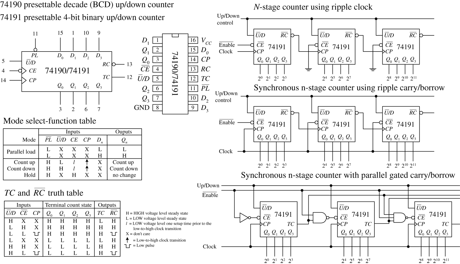
FIGURE 12.92
Presettable 4-Bit (MOD-16) Synchronous Up/Down Counter
The 74160 and 74163 resemble the 74190 and 74191 but require no external gates when used in multistage counter configurations. Instead, you simply cascade counter ICs together, as shown in Fig. 12.93.
For both devices, a count can be preset by applying the desired count to the D0 to D3 inputs and then applying a low to the parallel enable input 
![]() ; the input number is loaded into the counter on the next low-to-high clock transition. The master reset
; the input number is loaded into the counter on the next low-to-high clock transition. The master reset 
![]() is used to force all Q output low, regardless of the other input signals. The two clock enable inputs (CEP and CET) must be high for counting to begin. The terminal count output (TC) is forced high when the maximum count is reached, but will be forced low if CET goes low. This is an important feature that makes the multistage configuration synchronous, while avoiding the need for external gating. The truth tables along with the example load, count-up, and count-down timing sequences in Figs. 12.93 and 12.94 should help you better understand how these two devices work.
is used to force all Q output low, regardless of the other input signals. The two clock enable inputs (CEP and CET) must be high for counting to begin. The terminal count output (TC) is forced high when the maximum count is reached, but will be forced low if CET goes low. This is an important feature that makes the multistage configuration synchronous, while avoiding the need for external gating. The truth tables along with the example load, count-up, and count-down timing sequences in Figs. 12.93 and 12.94 should help you better understand how these two devices work.
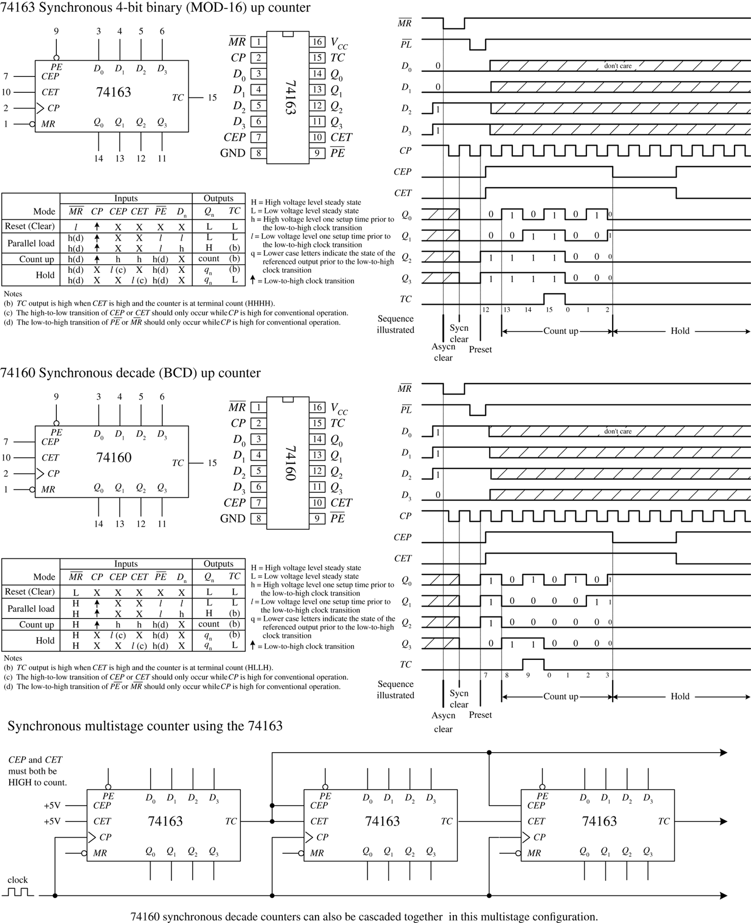
FIGURE 12.93
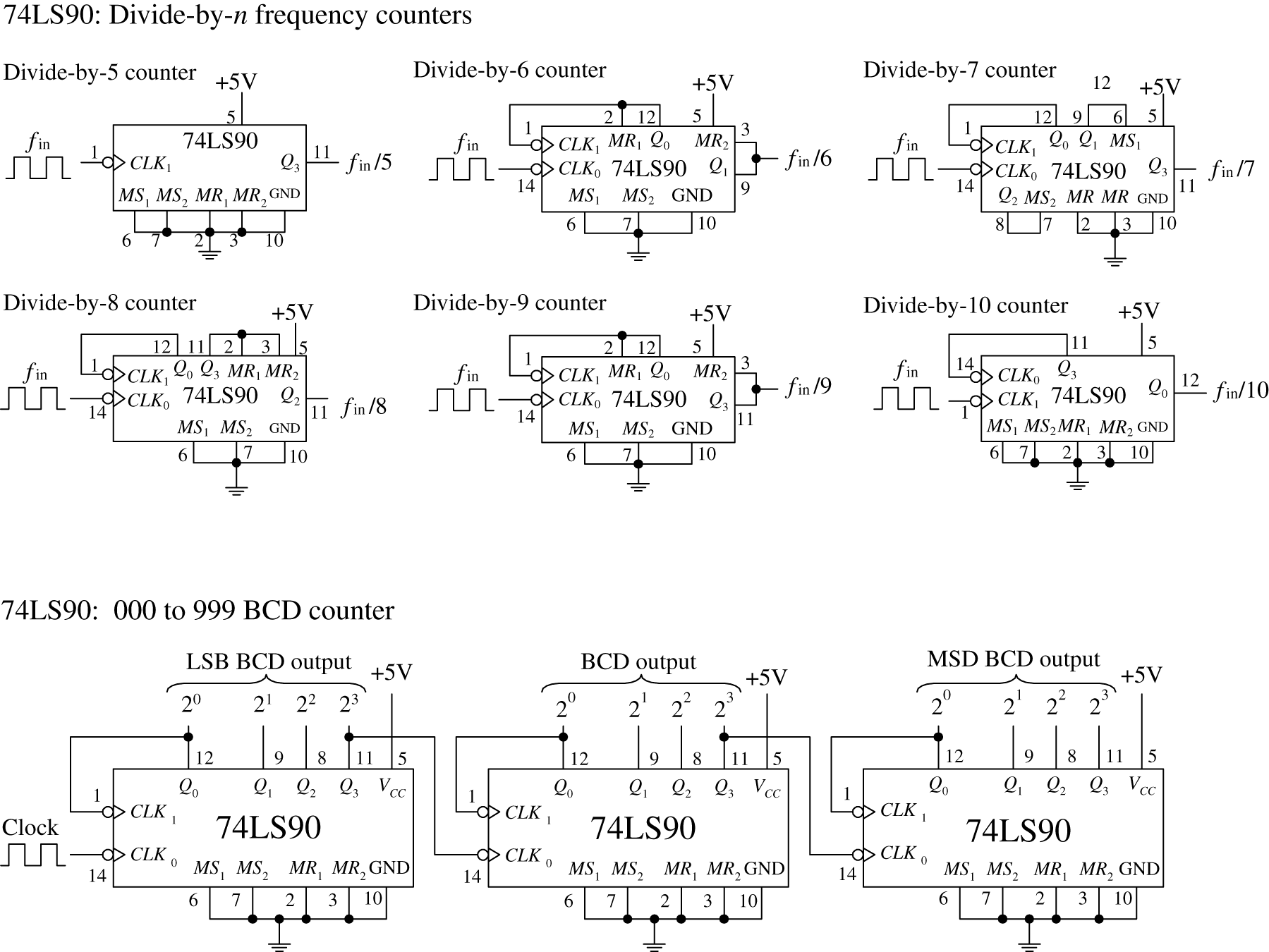
FIGURE 12.94
12.7.3 A Note on Counters with Displays
If you want to build a fairly sophisticated counter that can display many digits, the previous techniques are not worth pursuing, because there are simply too many discrete components to work with (for example, a separate seven-segment decoder/driver for each digit). A common alternative approach is to use a microcontroller or FPGA that functions both as a counter and a display driver.
What microcontrollers and FPGAs can do that discrete circuits have a hard time achieving is multiplex a display. In a multiplexed system, corresponding segments of each digit of a multidigit display are linked together, while the common lines for each digit are brought out separately. You can see that the number of lines is significantly reduced; a nonmultiplexed 7-segment 4-digit display has 28 segment lines and 4 common lines, while the 4-digit multiplexed display has only 7 + 4, or 11, lines.
The trick to multiplexing involves flashing each digit, one after the other (and recycling), in a fast enough manner to make it appear that the display is continuously lit. In order to multiplex, the microcontroller's program must supply the correct data to the segment lines at the same time that it enables a given digit via a control signal sent to the common lead of that digit. We will talk about multiplexing displays in greater detail in Chap. 13 with microcontrollers and Chap. 14 using FPGAs.
60-Hz, 10-Hz, and 1-Hz Clock-Pulse Generator
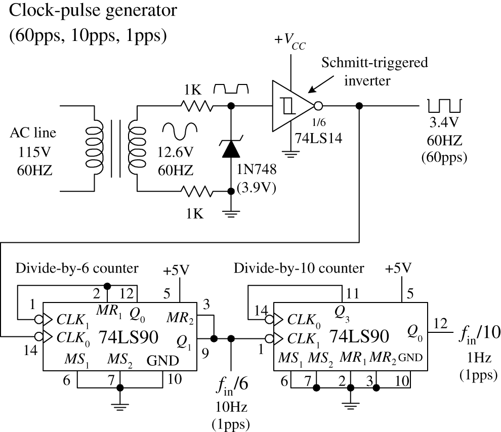
FIGURE 12.95
This simple clock-pulse generator provides a unique way to generate 60-, 10-, and 1-Hz clock signals that can be used in applications that require real-time counting. The basic idea is to take the characteristic 60-Hz ac line voltage (from the wall socket) and convert it into a lower-voltage squarewave of the same frequency. (Note that countries other than the United States typically use 50 Hz instead of 60 Hz. For 50 Hz operation, use an appropriate transformer and replace the divide-by-6 counter with the divide-by-5 counter shown in the upper left of Fig. 12.94.) First, the ac line voltage is stepped down to 12.6 V by the transformer. The negative-going portion of the 12.6-V ac voltage is removed by the zener diode (which acts as a half-wave rectifier). At the same time, the zener diode clips the positive-going signal to a level equal to its reverse breakdown voltage (3.9 V). This prevents the Schmitt-triggered inverter from receiving an input level that exceeds its maximum input rating. The Schmitt-triggered inverter takes the rectified/chipped sine wave and converts it into a true squarewave. The Schmitt trigger's output goes low (∼0.2 V) when the input voltage exceeds its positive threshold voltage VT+ (∼1.7 V) and goes high (∼3.4 V) when its input falls below its negative threshold voltage VT- (∼0.9 V). From the inverter's output, you get a 60-Hz squarewave (or a clock signal beating out 60 pulses per second). To get a 10-Hz clock signal, you slap on a divide-by-6 counter. To get a 1-Hz signal, you slap a divide-by-10 counter onto the output of the divide-by-6 counter.
Another approach used to create multidigit counters is to use a multidigit counter/display driver IC. One such IC is the ICM7217, a four-digit LED display programmable up/down counter made by Intersil. This device is typically used in hardwired applications where thumbwheel switches are used to load data and SPDT switches are used to control the chip. The ICM7217A provides multiplexed seven-segment LED display outputs that are used to drive common cathode displays.
A simple application of the ICM7217A is a four-digit unit counter shown in Fig. 12.96. If you are interested in knowing all the specifics of how this counter works, along with learning about other applications for this device, check out Maxim's data sheets at http://www.maxim-ic.com/datasheet/index.mvp/id/1501. It is better to learn from the maker in this case. Also, take a look at the other counter/display driver ICs Maxim has to offer. Other manufacturers produce similar devices, so visit their websites as well.
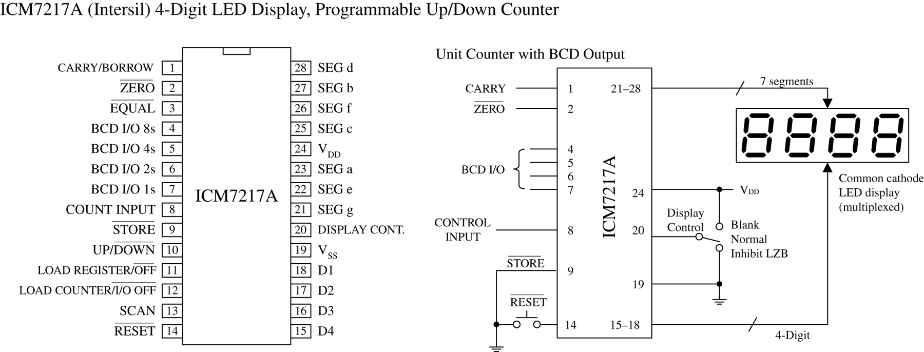
FIGURE 12.96
12.8 Shift Registers
Data words traveling through a digital system frequently must be temporarily held, copied, and bit-shifted to the left or to the right. A device that can be used for such applications is the shift register. A shift register is constructed from a row of flip-flops connected so that digital data can be shifted down the row either in a left or right direction. Most shift registers can handle parallel movement of data bits as well as serial movement, and also can be used to convert from parallel to serial or from serial to parallel. Figure 12.97 shows several types of shift register arrangements: serial-in/serial-out, parallel-in/serial-out, and serial-in/parallel out.
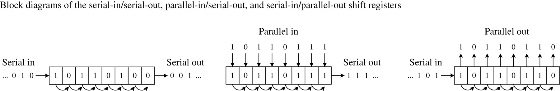
FIGURE 12.97
12.8.1 Serial-In/Serial-Out Shift Registers
Figure 12.98 shows a simple 4-bit serial-in/serial-out shift register made from D flip-flops. Serial data is applied to the D input of flip-flop 0. When the clock line receives a positive clock edge, the serial data is shifted to the right from flip-flop 0 to flip-flop 1. Whatever bits of data were present at flip-flop 2's, 3's, and 4's outputs are shifted to the right during the same clock pulse. To store a 4-bit word into this register requires four clock pulses. The rightmost circuit shows how you can rewire the flip-flops to make a shift-left register. To make larger bit-shift registers, more flip-flops are added (for example, an 8-bit shift register would require eight flip-flops cascaded together).
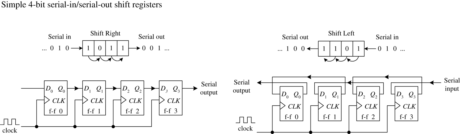
FIGURE 12.98
12.8.2 Serial-In/Parallel-Out Shift Registers
Figure 12.99 shows a 4-bit serial-in/parallel-out shift register constructed from D flip-flops. This circuit is essentially the same as the previous serial-in/serial-out shift register, except now you attach parallel output lines to the outputs of each flip-flop as shown. Note that this shift register circuit also comes with an active-low clear input 
![]() and a strobe input that acts as a clock enable control. The timing diagram in the figure shows a sample serial-to-parallel shifting sequence.
and a strobe input that acts as a clock enable control. The timing diagram in the figure shows a sample serial-to-parallel shifting sequence.
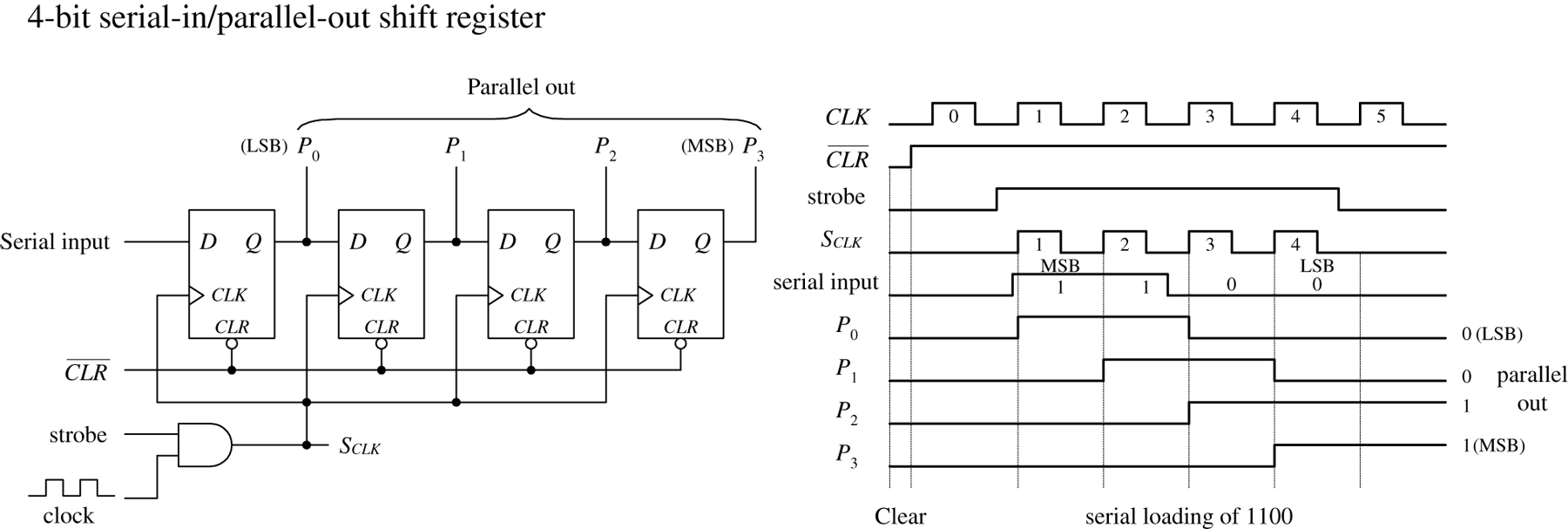
FIGURE 12.99
12.8.3 Parallel-In/Serial-Out Shift Registers
Constructing a 4-bit parallel-to-serial shift register from D flip-flops requires some additional control logic, as shown in the circuit in Fig. 12.100. Parallel data must first be loaded into the D inputs of all four flip-flops. To load data, the SHIFT/ 
![]() is made low. This enables the AND gates with X marks, allowing the 4-bit parallel input word to enter the D0–D3 inputs of the flip-flops. When strobe and CLK are both high, the 4-bit parallel word is latched simultaneously into the four flip-flops and appears at the Q0–Q3 outputs. To shift the latched data out through the serial output, the SHIFT/
is made low. This enables the AND gates with X marks, allowing the 4-bit parallel input word to enter the D0–D3 inputs of the flip-flops. When strobe and CLK are both high, the 4-bit parallel word is latched simultaneously into the four flip-flops and appears at the Q0–Q3 outputs. To shift the latched data out through the serial output, the SHIFT/ ![]() line is made high. This enables all unmarked AND gates, allowing the latched data bit at the Q output of a flip-flop to pass (shift) to the D input of the flip-flop to the right. In this shift mode, four clock pulses are required to shift the parallel word out of the serial output.
line is made high. This enables all unmarked AND gates, allowing the latched data bit at the Q output of a flip-flop to pass (shift) to the D input of the flip-flop to the right. In this shift mode, four clock pulses are required to shift the parallel word out of the serial output.
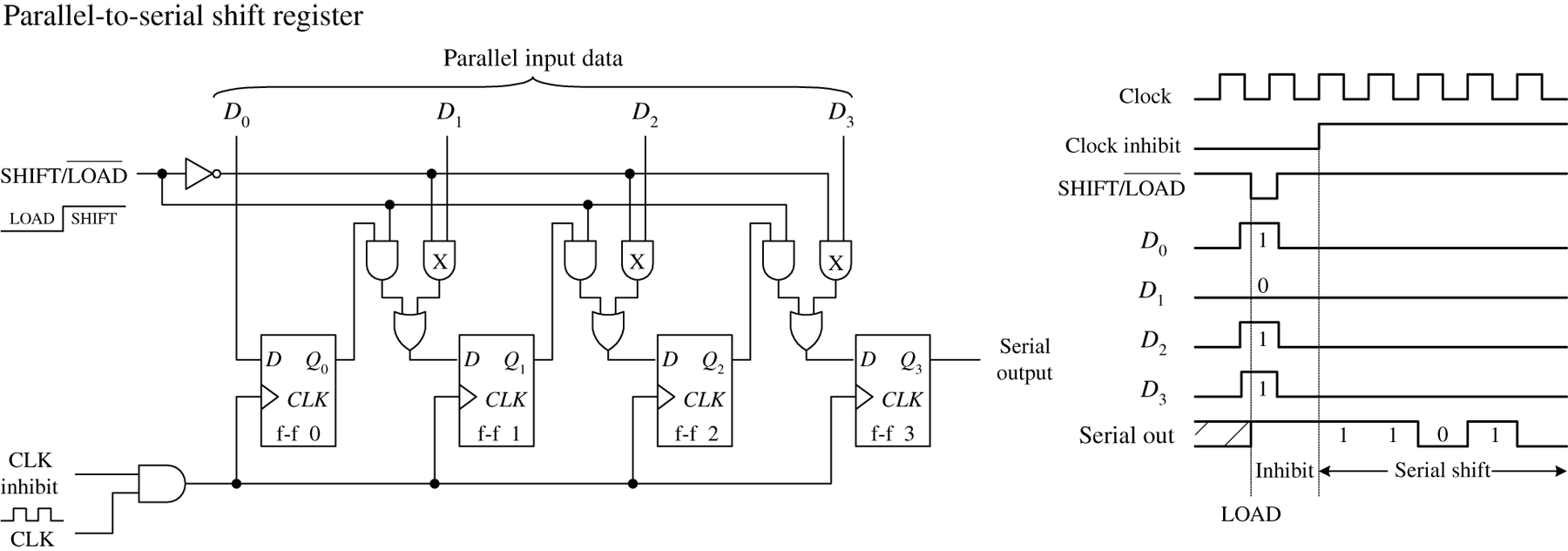
FIGURE 12.100
12.8.4 Ring Counter (Shift Register Sequencer)
The ring counter (shift register sequencer) is a unique type of shift register that incorporates feedback from the output of the last flip-flop to the input of the first flip-flop. Figure 12.101 shows a 4-bit ring counter made from D-type flip-flops. In this circuit, when the 
![]() input is set low, Q0 is forced high by the active-low preset, while Q1, Q2, and Q3 are forced low (cleared) by the active-low clear. This causes the binary word 1000 to be stored within the register. When the
input is set low, Q0 is forced high by the active-low preset, while Q1, Q2, and Q3 are forced low (cleared) by the active-low clear. This causes the binary word 1000 to be stored within the register. When the ![]() line is brought low, the data bits stored in the flip-flops are shifted right with each positive clock edge. The data bit from the last flip-flop is sent to the D input of the first flip-flop. The shifting cycle will continue to recirculate while the clock is applied. To start a fresh cycle, the
line is brought low, the data bits stored in the flip-flops are shifted right with each positive clock edge. The data bit from the last flip-flop is sent to the D input of the first flip-flop. The shifting cycle will continue to recirculate while the clock is applied. To start a fresh cycle, the ![]() line is momentarily brought low.
line is momentarily brought low.
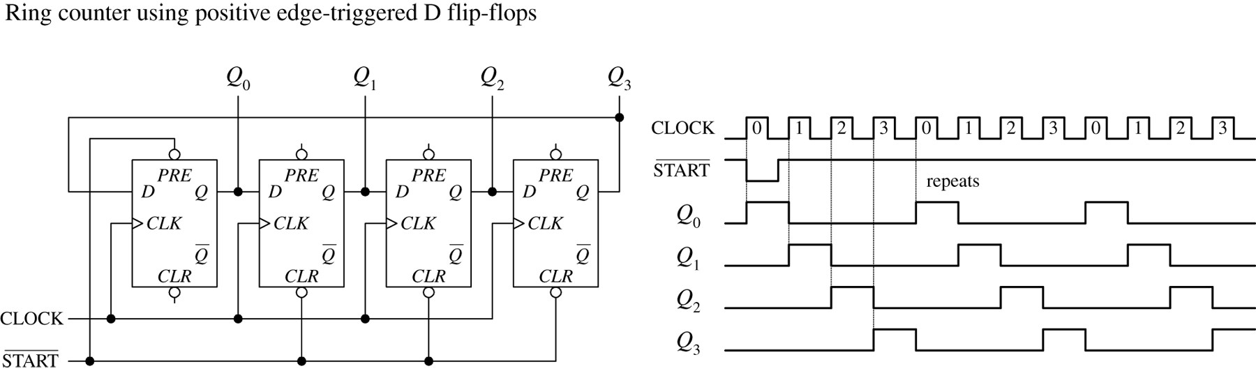
FIGURE 12.101
12.8.5 Johnson Shift Counter
The Johnson shift counter is similar to the ring counter except that its last flip-flop feeds data back to the first flip-flop from its inverted output ( 
![]() ). For this reason, this type is sometimes called a Moebius counter, as the bit sequence will be shifted out first "normally," then inverted, then normally, and so on. In the simple 4-bit Johnson shift counter shown in Fig. 12.102, you start out by applying a low to the
). For this reason, this type is sometimes called a Moebius counter, as the bit sequence will be shifted out first "normally," then inverted, then normally, and so on. In the simple 4-bit Johnson shift counter shown in Fig. 12.102, you start out by applying a low to the ![]() line, which sets presets Q0 high; Q1, Q2, and Q3 low; and
line, which sets presets Q0 high; Q1, Q2, and Q3 low; and 
![]() high. In other words, you load the register with the binary word 1000, as you did with the ring counter.
high. In other words, you load the register with the binary word 1000, as you did with the ring counter.
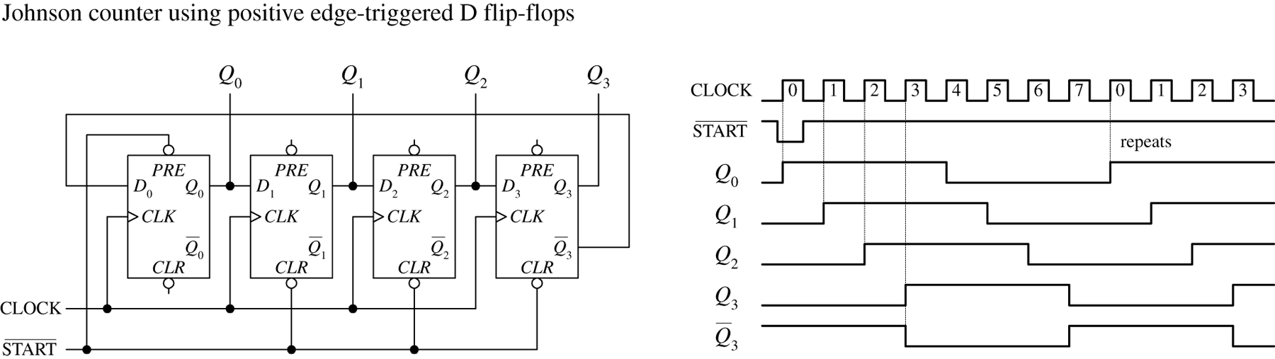
FIGURE 12.102
Now, when you bring the ![]() line low, data will shift through the register. However, unlike the ring counter, the first bit sent back to the D0 input of the first flip-flop will be high because feedback is from
line low, data will shift through the register. However, unlike the ring counter, the first bit sent back to the D0 input of the first flip-flop will be high because feedback is from ![]() not Q3. At the next clock edge, another high is fed back to D0; at the next clock edge, another high is fed back; at the next edge, another high is fed back. Only after the fourth clock edge does a low get fed back (the 1 has shifted down to the last flip-flop and
not Q3. At the next clock edge, another high is fed back to D0; at the next clock edge, another high is fed back; at the next edge, another high is fed back. Only after the fourth clock edge does a low get fed back (the 1 has shifted down to the last flip-flop and ![]() goes high). At this point, the shift register is full of 1s.
goes high). At this point, the shift register is full of 1s.
As more clock pulses arrive, the feedback loop supplies lows to D0 for the next four clock pulses. After that, the Q outputs of all the flip-flops are low, while ![]() goes high. This high from
goes high. This high from ![]() is fed back to
is fed back to 
![]() during the next positive clock edge, and the cycle repeats.
during the next positive clock edge, and the cycle repeats.
As you can see, the 4-bit Johnson shift counter has eight output stages (which require eight clock pulses to recycle), not four, as is the case with the ring counter.
12.8.6 Shift Register ICs
Now that we have covered the basic theory of shift registers, let's take a look at practical shift register ICs that contain all the necessary logic circuitry inside. It is not uncommon for a serial to parallel shift register IC to be used with a microcontroller to provide it with more outputs when driving LEDs. The serial data is fed into the shift register and then the output latched to turn the LEDs on or off.
7491A 8-Bit Serial-In/Serial-Out Shift Register IC
The 7491A is an 8-bit serial-in/serial-out shift register that consists of eight internally linked SR flip-flops. This device has positive edge-triggered inputs and a pair of data inputs (A and B) that are internally ANDed together, as shown in the logic diagram in Fig. 12.103. This type of data input means that for a binary 1 to be shifted into the register, both data inputs must be high. For a binary 0 to be shifted into the register, either input can be low. Data is shifted to the right at each positive clock edge.
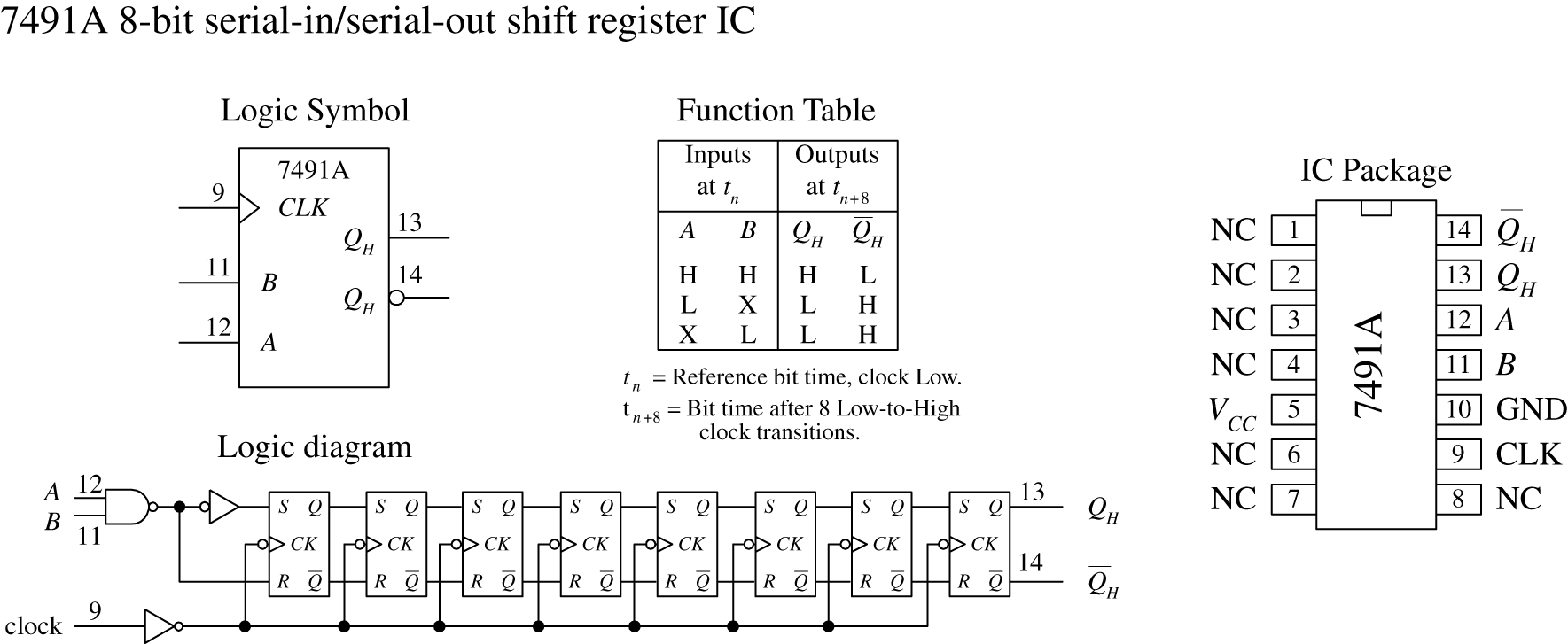
FIGURE 12.103
74164 8-Bit Serial-In/Parallel-Out Shift Register IC
The 74164 is an 8-bit serial-in/parallel-out shift register. It contains eight internally linked flip-flops and has two serial inputs, Dsa and Dsb, which are ANDed together. Like the 7491A, the unused serial input acts as an enable/disable control for the other serial input. For example, if you use Dsa as the serial input, you must keep Dsb high to allow data to enter the register, or you can keep it low to prevent data from entering the register.
Data bits are shifted one position to the right at each positive clock edge. The first data bit entered will end up at the Q7 parallel output after the eighth clock pulse. The master reset 
![]() resets all internal flip-flops and forces the Q outputs low when it is pulsed low.
resets all internal flip-flops and forces the Q outputs low when it is pulsed low.
In the sample circuit shown in Fig. 12.104, a serial binary number 10011010 (15410) is converted into its parallel counterpart. Note the AND gate and strobe input used in this circuit. The strobe input acts as a clock enable input; when it is set high, the clock is enabled. The timing diagram paints the rest of the picture.
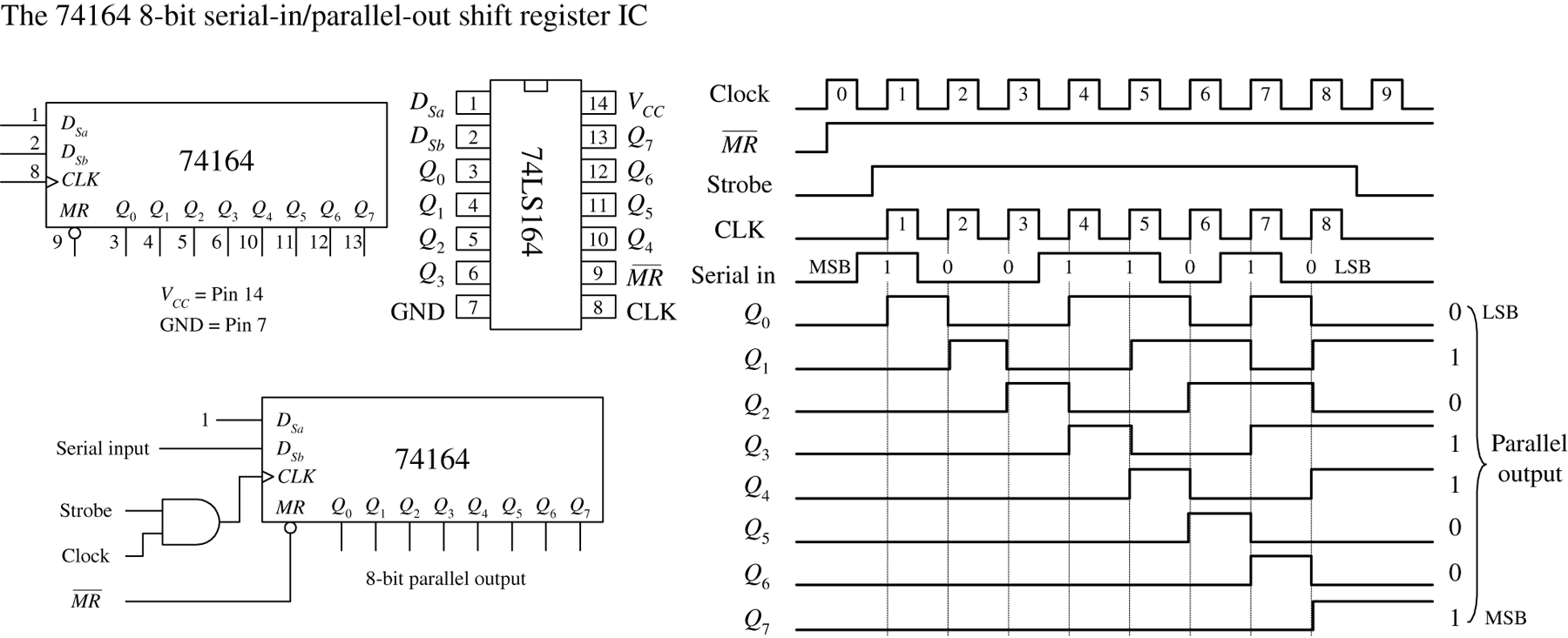
FIGURE 12.104
75165 8-Bit Serial-In or Parallel-In/Serial-Out Shift Register IC
The 75165 is a unique 8-bit device that can act as either a serial-to-serial shift register or as a parallel-to-serial shift register. When used as a parallel-to-serial shift register, parallel data is applied to the D0–D7 inputs and then loaded into the register when the parallel load input 
![]() is pulsed low. To begin shifting the loaded data out of the serial output Q7 (or
is pulsed low. To begin shifting the loaded data out of the serial output Q7 (or 
![]() if you want inverted bits), the clock enable input
if you want inverted bits), the clock enable input 
![]() must be set low to allow the clock signal to reach the clock inputs of the internal D-type flip-flops. When used as a serial-to-serial shift register, serial data is applied to the serial data input DS. A sample shift, load, and inhibit timing sequence is shown in Fig. 12.105.
must be set low to allow the clock signal to reach the clock inputs of the internal D-type flip-flops. When used as a serial-to-serial shift register, serial data is applied to the serial data input DS. A sample shift, load, and inhibit timing sequence is shown in Fig. 12.105.
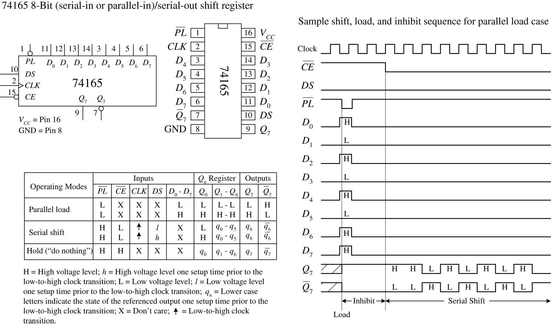
FIGURE 12.105
74194 Universal Shift Register IC
Figure 12.106 shows the 74194 4-bit bidirectional universal shift register. This device can accept either serial or parallel inputs, provide serial or parallel outputs, and shift left or right based on input signals applied to select controls S0 and S1. Serial data can be entered into either the serial shift-right input (DSR) or the serial shift-left input (DSL). Select controls S0 and S1 are used to initiate a hold (S0 = low, S1 = low), shift left (S0 = low, S1 = high), shift-right (S0 = high, S1 = low), or to parallel load (S0 = high, S1 = high) mode. A clock pulse must then be applied to shift or parallel load the data.
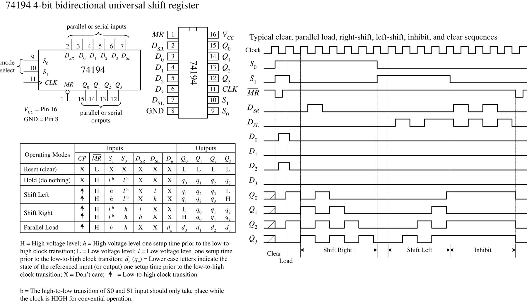
FIGURE 12.106
In parallel load mode (S0 and S1 are high), parallel input data is entered via the D0 through D3 inputs and transferred to the Q0 to Q3 outputs following the next low-to-high clock transition. The 74194 also has an asynchronous master reset 
![]() input that forces all Q outputs low when pulsed low. To make a shift-right recirculating register, the Q3 output is wired back to the DSR input, while making S0 = high and S1 = low. To make a shift-left recirculating register, the Q0 output is connected back to the DSL input, while making S0 = low and S1 = high. The timing diagram in Fig. 12.106 shows a typical parallel load and shifting sequence.
input that forces all Q outputs low when pulsed low. To make a shift-right recirculating register, the Q3 output is wired back to the DSR input, while making S0 = high and S1 = low. To make a shift-left recirculating register, the Q0 output is connected back to the DSL input, while making S0 = low and S1 = high. The timing diagram in Fig. 12.106 shows a typical parallel load and shifting sequence.
74299 8-Bit Universal Shift/Storage Register with Three-State Interface
A number of shift registers have three-state outputs—outputs that can assume a high, low, or high impedance state (open-circuit or float state). These devices are commonly used as storage registers in three-state bus interface applications.
An example 8-bit universal shift/storage register with three-state outputs is the 74299, shown in Fig. 12.107. This device has four synchronous operating modes that are selected via two select inputs, S0 and S1. Like the 74194 universal shift register, the 74299's select modes include shifting right, shifting left, holding, and parallel loading (see the function table in Fig. 12.107). The mode-select inputs, serial data inputs (DS0 and DS7), and parallel-data inputs (I/O0 through I/O7) are positive edge triggered. The master reset ![]() input is an asynchronous active-low input that clears the register when pulsed low.
input is an asynchronous active-low input that clears the register when pulsed low.
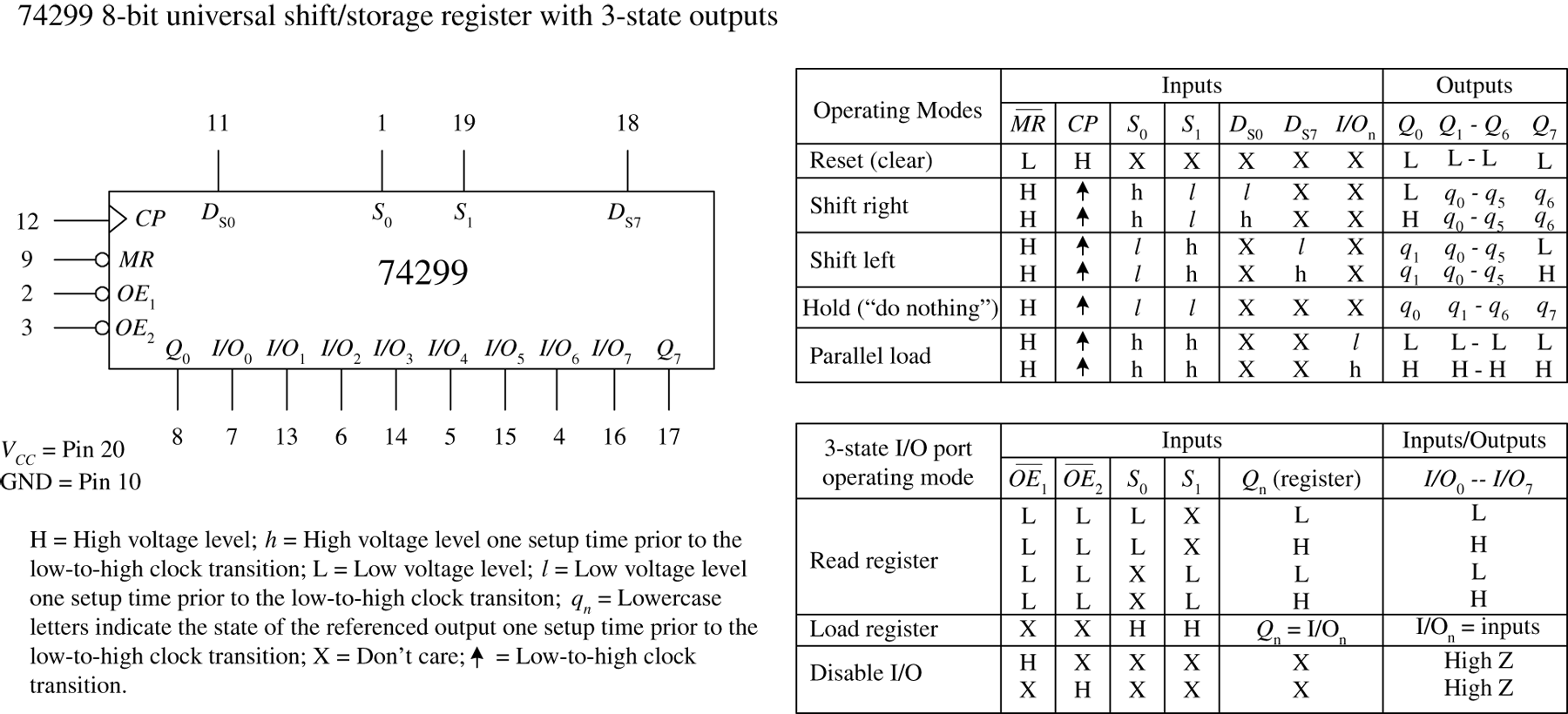
FIGURE 12.107
The three-state bidirectional I/O port has three modes of operation:
- The read-register mode allows data within the register to be available at the I/O outputs. This mode is selected by making both output-enable inputs (

 and
and 
 ) low and making one or both select inputs low.
 - The load-register mode sets up the register for a parallel load during the next low-to-high clock transition. This mode is selected by setting both select inputs high.
- The disable-I/O mode acts to disable the outputs (set to a high impedance state) when a high is applied to one or both of the output-enable inputs. This effectively isolates the register from the bus to which it is attached.
12.8.7 Simple Shift Register Applications
16-Bit Serial-to-Parallel Converter
A simple way to create a 16-bit serial-to-parallel converter is to join two 74164 8-bit serial-in/parallel-out shift registers, as shown in Fig. 12.108. To join the two ICs, simply wire the Q7 output from the first register to one of the serial inputs of the second register. (Recall that the serial input that is not used for serial input data acts as an active-high enable control for the other serial input.)
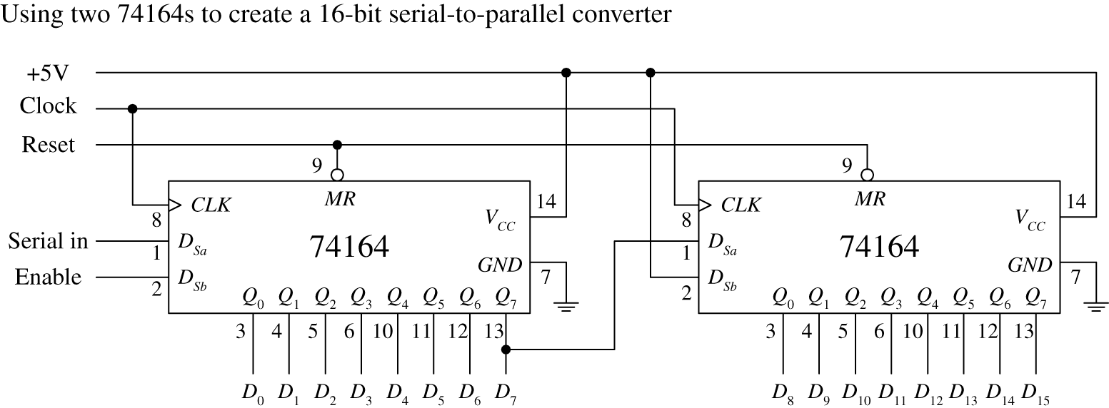
FIGURE 12.108
In terms of operation, when data is shifted out of Q7 of the first register (or data output D7), it enters the serial input of the second (the example uses DSa as the serial input) and will be presented to the Q0 output of the second register (or data output D8). For an input data bit to reach the Q7 output of the second register (or data output D15), 16 clock pulses must be applied.
8-Bit Serial-to-Parallel Converter with Simultaneous Data Transfer
Figure 12.109 shows a circuit that acts as a serial-to-parallel converter that outputs the converted 8-bit word only when all 8 bits have been entered into the register. Here, a 74164 8-bit serial-in/parallel-out shift register is used, along with a 74HCT273 octal D-type flip-flop and a divide-by-8 counter. At each positive clock edge, the serial data is loaded into the 74164. After eight clock pulses, the first serial bit entered is shifted down to the 74164's Q7 output, while the last serial bit entered resides at the 74164's Q0 output. At the negative edge of the eighth clock pulse, the negative-edge triggered divide-by-8 circuit's output goes high. During this high transition, the data present on the inputs of the 74HCT273 (which hold the same data present at the 74164's Q outputs) is passed to the 74HCT273's outputs at the same time. (Think of the 74HCT273 as a temporary storage register that dumps its contents after every eighth clock pulse.)
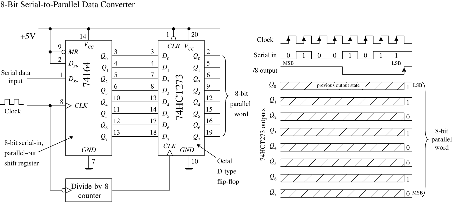
FIGURE 12.109
8-Bit Parallel-to-Serial Interface
Figure 12.110 shows a 74165 8-bit parallel-to-serial shift register used to accept a parallel ASCII word and convert it into a serial ASCII word that can be sent to a serial device. Recall that ASCII codes are only 7 bits long (for example, the binary code for & is 010 0110). How do you account for the missing bit? As it turns out, most 8-bit devices communicating via serial ASCII will use an additional eighth bit for a special purpose, perhaps to act as a parity bit or as a special function bit to enact a special set of characters. Often, the extra bit is simply set low and ignored by the serial device receiving it.
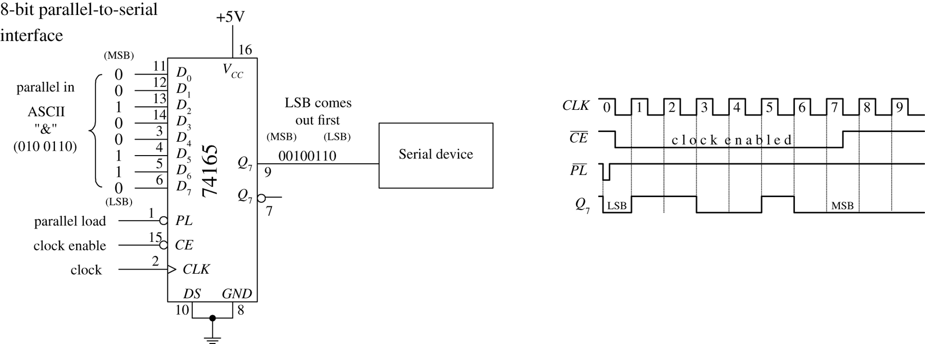
FIGURE 12.110
To keep things simple, let's set the extra bit low and assume that is how the serial device likes things done. This means that you will set the D0 input of the 74165 low. The MSB of the ASCII code will be applied to the D1 input, while the LSB of the ASCII code will be applied to the D7 input. Now, with the parallel ASCII word applied to the inputs of the register, when you pulse the parallel load line ( 
![]() ) low, the ASCII word, along with the "ignored bit," is loaded into the register. Next, you must enable the clock to allow the loaded data to be shifted out serially, by setting the clock enable input (
) low, the ASCII word, along with the "ignored bit," is loaded into the register. Next, you must enable the clock to allow the loaded data to be shifted out serially, by setting the clock enable input ( 
![]() ) low for the duration it takes for the clock pulses to shift out the parallel word. After the eighth clock pulse (0 to 7), the serial device will have received all 8 serial data bits. Practically speaking, a microprocessor or microcontroller is necessary to provide the
) low for the duration it takes for the clock pulses to shift out the parallel word. After the eighth clock pulse (0 to 7), the serial device will have received all 8 serial data bits. Practically speaking, a microprocessor or microcontroller is necessary to provide the ![]() and
and ![]() lines with the necessary control signals to ensure that the register and serial device communicate properly.
lines with the necessary control signals to ensure that the register and serial device communicate properly.
Recirculating Memory Registers
A recirculating memory register is a shift register that is preloaded with a binary word that is serially recirculated through the register via a feedback connection from the output to the input. Recirculating registers can be used for a number of applications, from supplying a specific repetitive waveform used to drive IC inputs to driving output drivers used to control stepper motors.
In the leftmost circuit in Fig. 12.111, a parallel 4-bit binary word is applied to the D0 to D3 inputs of a 74194 universal shift register. When the S1 select input is brought high (switch opened), the 4-bit word is loaded into the register. When the S1 input is then brought low (switch closed), the 4-bit word is shifted in a serial fashion through the register, out Q3, and back to Q0 via the DSR input (serial shift-right input) as positive clock edges arrive. Here, the shift register is loaded with 0111. As you begin shifting the bits through the register, a single low output will propagate down through high outputs, which in turn causes the LED attached to the corresponding low output to turn on. In other words, you have made a simple Christmas tree flasher.
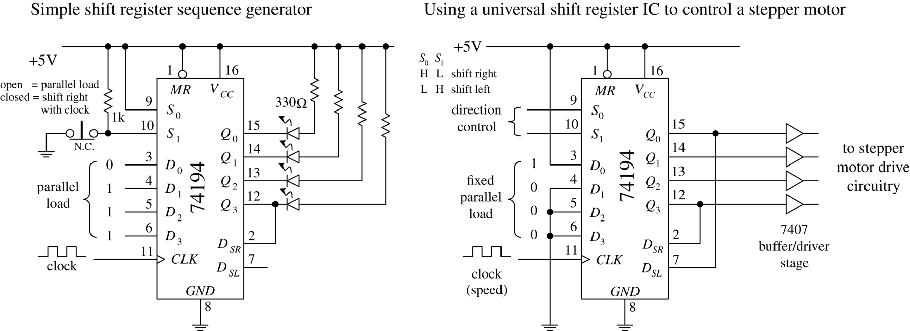
FIGURE 12.111
The rightmost circuit in Fig. 12.111 is basically the same thing as the leftmost circuit. However, now the circuit is used to drive a stepper motor. Typically, a stepper motor has four stator coils that must be energized in sequence to make the motor turn at a given angle. For example, to make a simple stepper motor turn clockwise, you must energize its stator coils 1, 2, 3, and 4 in the following sequence: 1000, 0100, 0010, 0001, 1000, and so on. To make the motor go counterclockwise, apply the following sequence: 1000, 0001, 0010, 0100, 1000, and so on. You can generate these simple firing sequences with the 74194 by parallel loading the D0 to D3 inputs with the binary word 1000. To output the clockwise firing sequence, simply shift bits to the right by setting S0 = high and S1 = low. As clock pulses arrive, the 1000 present at the outputs will then become 0100, then 0010, 0001, 1000, and so on.
The speed of rotation of the motor is determined by the clock frequency. To output the counterclockwise firing sequence, simply shift bits to the left by setting S0 = low and S1 = high. To drive steppers, it is typically necessary to use a buffer/driver interface like the 7407 shown in Fig. 12.111, as well a number of output transistors, not shown. Also, different types of stepper motors may require different firing sequences than the one shown here. Stepper motors and the various circuits used to drive them are discussed in detail in Chap. 15.
12.9 Analog/Digital Interfacing
A number of tricks are used to interface analog circuits with digital circuits. In this section, we'll take a look at two basic levels of interfacing. One level deals with simple on/off triggering. The other level deals with true analog-to-digital and digital-to-analog conversion—converting analog signals into digital numbers and converting digital numbers into analog signals. These techniques are just as applicable to connecting things to the digital input pins of a microcontroller.
12.9.1 Triggering Simple Logic Responses from Analog Signals
There are times when you need to drive logic from simple on/off signals generated by analog devices. For example, you may want to latch an alarm (via a flip-flop) when an analog voltage—say, one generated from a temperature sensor—reaches a desired threshold level. Or perhaps you simply want to count the number of times a certain analog threshold is reached. For simple on/off applications such as these, it is common to use a comparator or op amp as the interface between the analog output of the transducer and the input of the logic circuit. Often it is possible to simply use a voltage divider network composed of a transducer of variable resistance and a pullup resistor. Figure 12.112 shows some sample networks to illustrate the point.
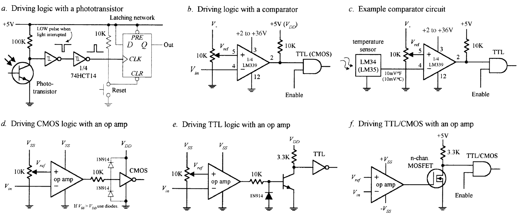
FIGURE 12.112
In Fig. 12.112a, a phototransistor is used to trigger a logic response. Normally, the phototransistor is illuminated, which keeps the input of the first Schmitt inverter low. The output of the second inverter is high. When the light is briefly interrupted, the phototransistor momentarily stops conducting, causing the input to the first inverter to pulse low, while the output of the second inverter pulses high. This high pulse could be used to latch a D flip-flop, which could be used to trigger an LED or a buzzer alarm.
In Fig. 12.112b, a single-supply comparator with open-collector output is used as an analog-to-digital interface. When an analog voltage applied to Vin exceeds the reference voltage (Vref) set at the noninverting input (+) via the pot, the output goes low (the comparator sinks current through itself to ground). When Vin goes below Vref, the output goes high (the comparator's output floats, but the pullup resistor pulls the comparator's output high).
In Fig. 12.112c, a simple application of the previous comparator interface is shown. The input voltage is generated by an LM34 or LM35 temperature sensor. The LM34 generates 10 mV/°F, while the LM35 generates 10 mV/°C. The resistance of the pot and V+ determine the reference voltage. If we want to drive the comparator low when 75°C is reached, we set the reference voltage to 750 mV, assuming we're using the LM35.
In Fig. 12.112d, an op amp set in comparator mode can also be used as an analog-to-digital interface for simple switching applications. CMOS logic can be driven directly through a current limiting resistor, as shown. If the supply voltage of the op amp exceeds the supply voltage of the logic, protection diodes should be used (as shown in the figure).
Protection diodes were not necessary with the LM339 because that has open-collector outputs.
In Fig. 12.112e, an op amp that is used to drive TTL typically uses a transistor output stage like the one shown here. The diode acts to prevent base-to-emitter reverse breakdown. When Vin exceeds Vref, the op amp's output goes low, the transistor turns off, and the logic input receives a high.
In Fig. 12.112f, an n-channel MOSFET transistor is used as an output stage to an op amp.
12.9.2 Using Logic to Drive External Loads
Driving simple loads such as LEDs, relays, buzzers, or any device that assumes either an on or off state is relatively simple. When driving such loads, it is important to first check the driving logic's current specifications—how much current, say, a gate can sink or source. After that, you determine how much current the device to be driven will require. If the device draws more current than the logic can source or sink, a high-power transistor typically can be used as an output switch. Figure 12.113 shows some sample circuits used to drive various loads.
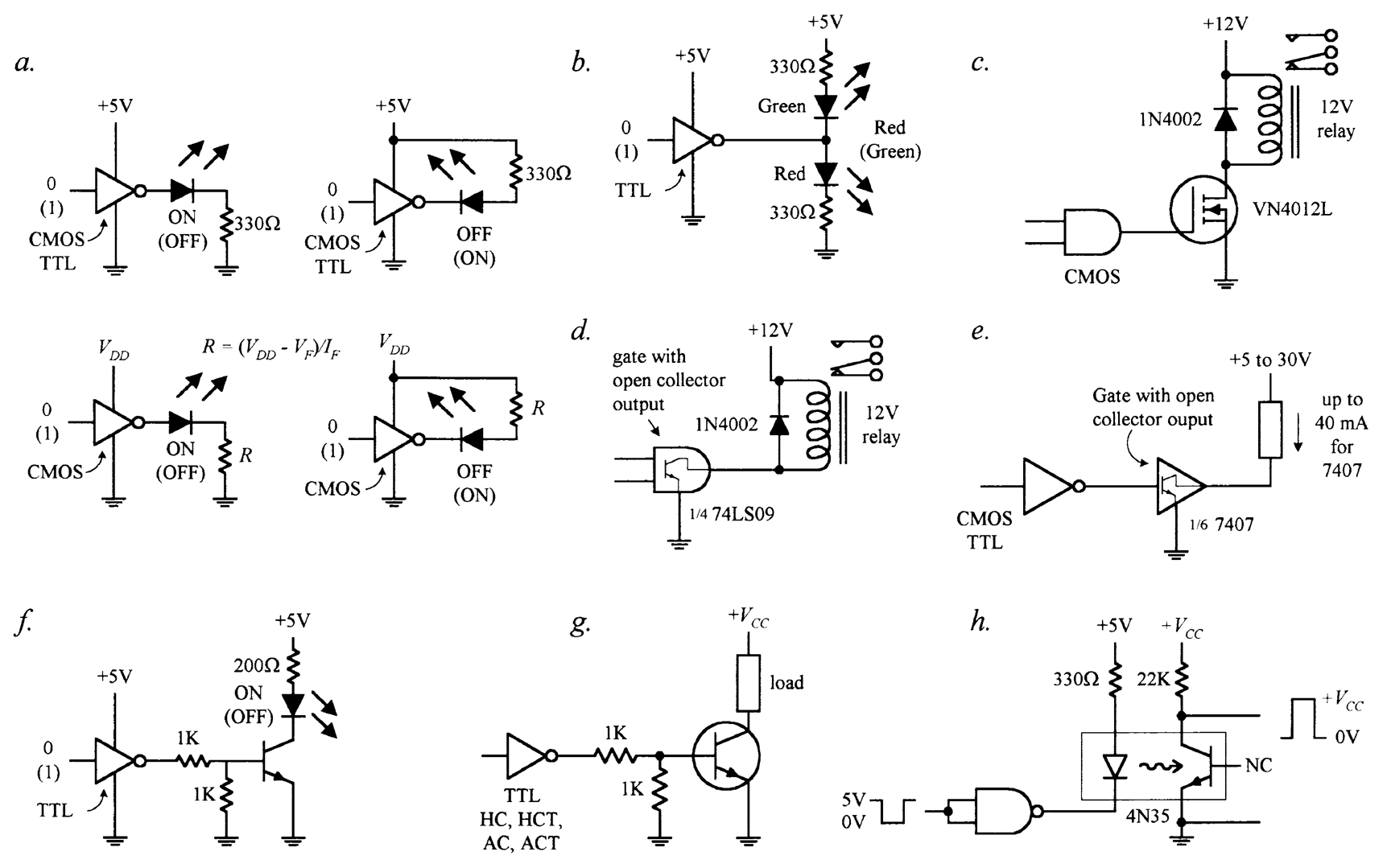
FIGURE 12.113
In Fig. 12.113a, LEDs can be driven directly by logic through a current-limiting resistor. Current can either be sourced or sunk. If an LED requires more current than the logic can supply or sink, a transistor output stage like the one shown in Fig. 12.113f can be used.
Figure 12.113b shows a simple way to get dual-lighting action from a pair of LEDs. When the gate's output goes low, the upper green LED turns on, while the lower red LED turns off. The LEDs switch states when the output goes high.
Relays will draw considerable current. To avoid damaging the logic device, in Fig. 12.113c, a power MOSFET transistor is attached to the logic output. The diode is used to protect the circuit from current spikes generated by relay as it switches states.
A handy method for interfacing standard logic with loads is to use a gate with an open-collector output as a go-between. Recall that open-collector gates cannot source current; they can only sink current. However, they typically can sink ten times the current of a standard logic gate. In Fig. 12.113d, an open-collector gate is used to drive a relay. Check the current ratings of specific open-collector devices before using them to be sure they can handle the load current.
Figure 12.113e shows another open-collector application. In Fig. 12.113f, a bipolar transistor is used to increase the output drive current used to drive a high-current LED. Make sure the transistor is of the proper current rating.
Figure 12.113g is basically the same as the previous example, but the load can be something other than an LED.
In Fig. 12.113h, an optocoupler is used to drive a load that requires electrical isolation from the logic driving it. Electrical isolation is often used in situations where external loads use a separate ground system. The voltage level at the load side of the optical interface can be set via VCC. There are many different types of optocouplers available (see Chap. 5).
12.9.3 Analog Switches
Analog switches are ICs designed to switch analog signals via digital control. The internal structure of these devices typically consists of a number of logic control gates interfaced with transistor stages used to control the flow of analog signals.
Figure 12.114 shows various types of analog switches. The CMOS 4066B quad bilateral switch uses a single-supply voltage from 3 to 15 V. It can switch analog or digital signals within ±7.5 V and has a maximum power dissipation of around 700 mW. Individual switches are controlled by digital inputs A through D. The TTL-compatible AH0014D DPDT analog switch can switch analog signals of ±10 V via the A and B logic control inputs. Note that this device has separate analog and digital supplies: V+ and V- are analog; VCC and GND are digital. The DG302A dual-channel CMOS DPST analog switch can switch analog signals within the ±10-V range at switching speeds up to 15 ns.
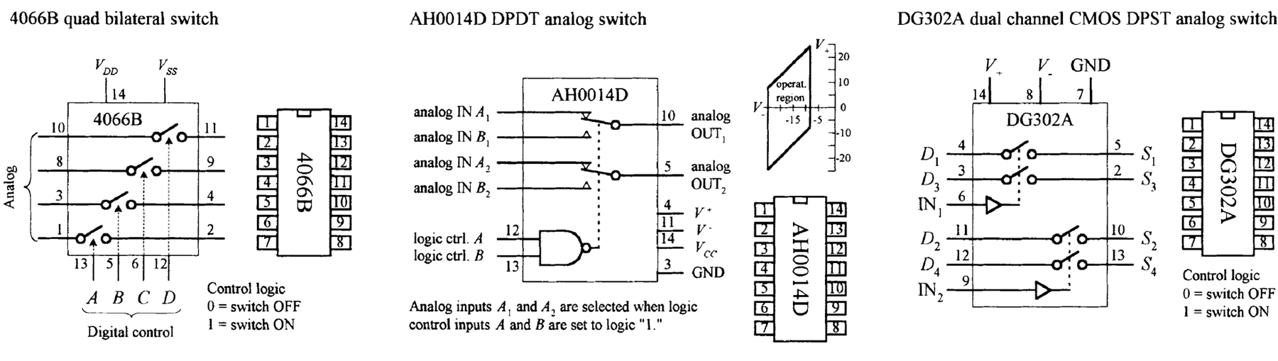
FIGURE 12.114
A number of circuits use analog switches. They are found in modulator/demodulator circuits, digitally controlled frequency circuits, analog signal-gain circuits, and analog-to-digital conversion circuits, where they often act as sample-hold switches. They can, of course, be used simply to turn a given analog device on or off.
12.9.4 Analog Multiplexer/Demultiplexer
Recall from Sec. 12.3 that a digital multiplexer acts like a data selector, while a digital demultiplexer acts like a data distributor. Analog multiplexers and demultiplexers act the same way but are capable of selecting or distributing analog signals. (They still use digital select inputs to select which pathways are open and which are closed to signal transmission.)
A popular analog multiplexer/demultiplexer IC is the 4051B, shown in Fig. 12.115. This device functions as either a multiplexer or demultiplexer, since its inputs and outputs are bidirectional (signals can flow in either direction). When used as a multiplexer, analog signals enter through I/O lines 0 through 7, while the digital code that selects which input is passed to the analog O/I line (pin 3) is applied to digital inputs A, B, and C. See the truth table in the figure. When used as a demultiplexer, the connections are reversed: The analog input comes in through the analog O/I line (pin 3) and passes out through one of the seven analog I/O lines. The specific output is again selected by the digital inputs A, B, and C. Note that when the inhibit line (INH) is high, none of the addresses are selected.
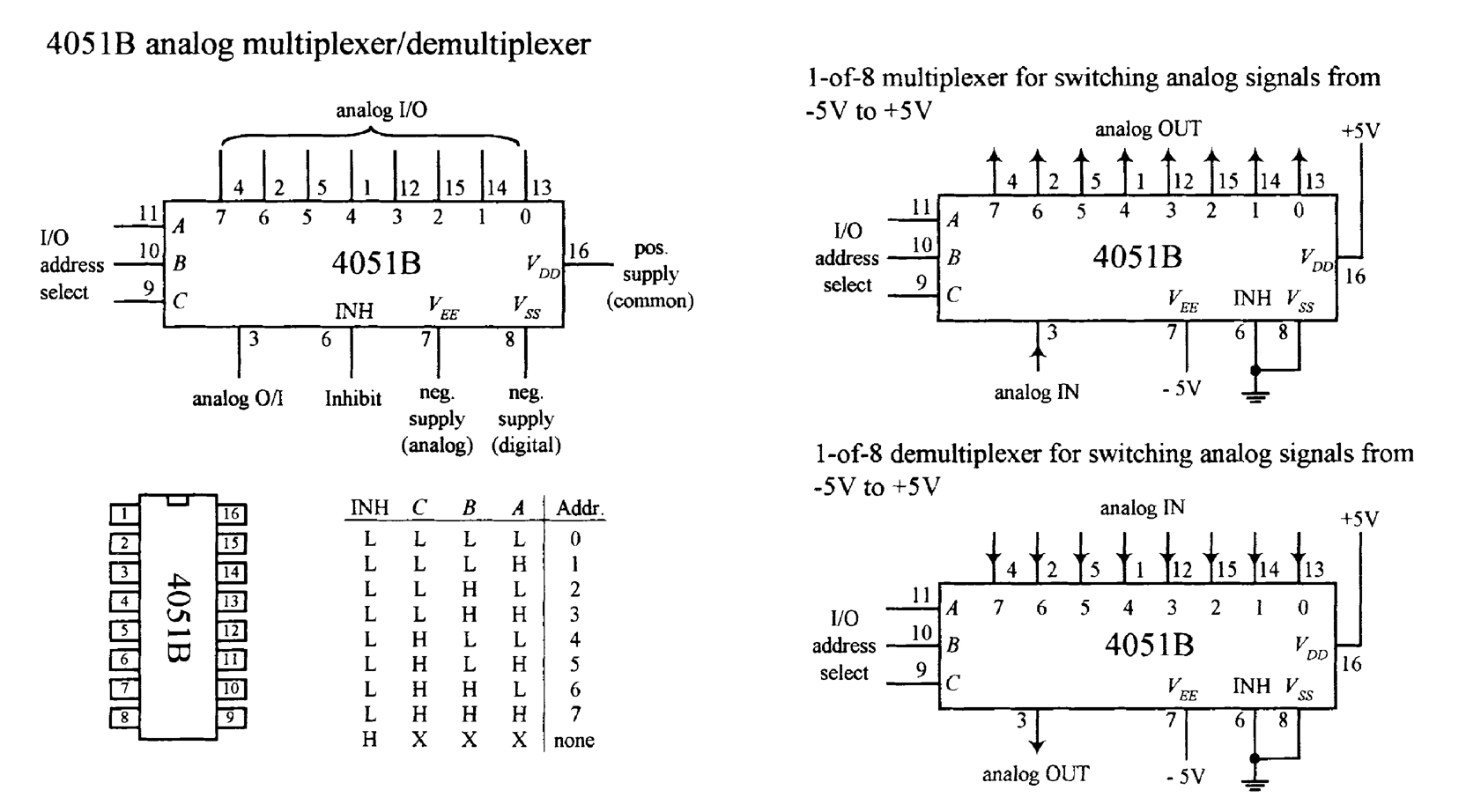
FIGURE 12.115
The I/O analog voltage levels for the 4051B are limited to a region between the positive supply voltage VDD and the analog negative supply voltage VEE. Note that the VSS supply is grounded. If the analog signals you are planning to use are all positive, VEE and VSS can both be connected to a common ground. However, if you plan to use analog voltages that range from, say, -5 to +5 V, VEE should be set to -5 V, while VDD should be set to +5 V. The 4051B accepts digital signals from 3 to 15 V, while allowing for analog signals from -15 to +15 V.
12.9.5 Analog-to-Digital and Digital-to-Analog Conversion
In order for analog devices (temperature sensors, strain gauges, position sensors, light meters, and so on) to communicate with digital circuits in a manner that goes beyond simple threshold triggering, we use an analog-to-digital converter (ADC). An ADC converts an analog signal into a series of binary numbers, each number proportional to the analog level measured at a given moment. Typically, the digital words generated by the ADC are fed into a microprocessor or microcontroller, where they can be processed, stored, interpreted, and manipulated. Analog-to-digital conversion is used in data-acquisition systems, digital sound recording, and within simple digital display test instruments (such as light meters and thermometers).
In order for a digital circuit to communicate with the analog world, we use a digital-to-analog converter (DAC). A DAC takes a binary number and converts it to an analog voltage that is proportional to the binary number. By supplying different binary numbers, one after the other, a complete analog waveform is created. DACs are commonly used to control the gain of an op amp, which in turn can be used to create digitally controlled amplifiers and filters. They are also used in waveform generator and modulator circuits and as trimmer replacements, and are found in a number of process-control and autocalibration circuits.
Many digital consumer products such as MP3 players, DVDs, and CD players use digital signal processing ADCs and DACs often contained in a microcontroller.
ADC and DAC Basics
Figure 12.116 shows the basic idea behind analog-to-digital and digital-to-analog conversion. In the analog-to-digital figure, the ADC receives an analog input signal along with a series of digital sampling pulses. Each time a sampling pulse is received, the ADC measures the analog input voltage and outputs a 4-bit binary number that is proportional to the analog voltage measured during the specific sample. With 4 bits, we get 16 binary codes (0000 to 1111) that correspond to 16 possible analog levels (for example, 0 to 15 V).
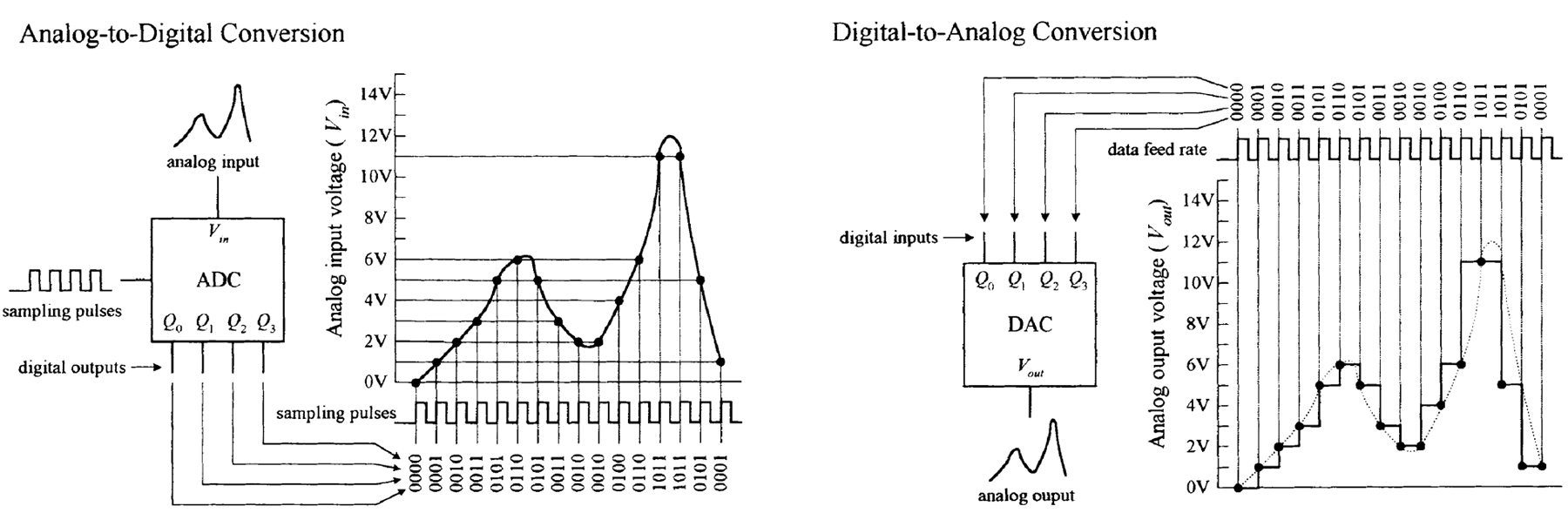
FIGURE 12.116
In the digital-to-analog conversion figure, the DAC receives a series of 4-bit binary numbers. The rate at which new binary numbers are fed into the DAC is determined by the logic that generates them. With each new binary number, a new analog voltage is generated. As with the ADC example, we have a total of 16 binary numbers to work with and 16 possible output voltages.
As you can see from the graphs, both these 4-bit converters lack the resolution needed to make the analog signal appear continuous (without steps). To make things appear more continuous, a converter with higher resolution is used. This means that instead of using 4-bit binary numbers, we use larger-bit numbers, such as 6-bit, 8-bit, 10-bit, 12-bit, 16-bit, or even 18-bit or higher numbers. If our converter has a resolution of 8 bits, we have 28 = 256 binary numbers to work with, along with 256 analog steps. Now, if this 8-bit converter is set up to generate 0 V at binary 00000000 and 15 V at binary 11111111 (full scale), then each analog step is only 0.058 V high (1⁄256 × 15 V). With an 18-bit converter, the steps get incredibly tiny because we have 218 = 262,144 binary numbers and steps. With 0 V corresponding to binary 000000000000000000 and 15 V corresponding to 111111111111111111, the 18-bit converter yields steps that are only 0.000058 V high! As you can see in the 18-bit case, the conversion process between digital and analog appears practically continuous.
Simple Binary-Weighted DAC
Figure 12.117 shows a simple 4-bit DAC that is constructed from a digitally controlled switch (74HC4066), a set of binary-weighted resistors, and an operational amplifier. The basic idea is to create an inverting amplifier circuit whose gain is controlled by changing the input resistance Rin. The 74HC4066 and the resistors together act as a digitally controlled Rin that can take on one of 16 possible values. You can think of the 74HC4066 and resistor combination as a digitally controlled current source. Each new binary code applied to the inputs of the 74HC4066 generates a new discrete current level that is summed by RF to provide a new discrete output voltage level.
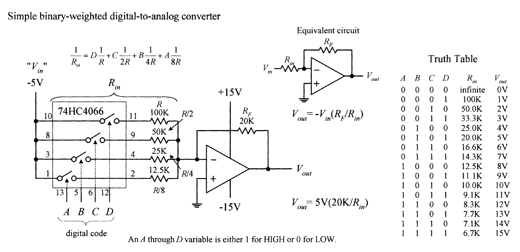
FIGURE 12.117
We choose scaled resistor values of R, R/2, R/4, and R/8 to give Rin discrete values that are equally spaced. To find all possible values of Rin, we use the formula provided in Fig. 12.117. This formula looks like the old resistors-in-parallel formula, but we must exclude those resistors that are not selected by the digital input code—that's what the coefficients A through D are for (a coefficient is either 1 or 0, depending on the digital input).
To find the analog output voltage, we simply use Vout = -Vref(RF/Rin)—the expression used for the inverting amplifier (see Chap. 8). Figure 12.117 shows what we get when we set Vref = -5 V, R = 100 kΩ, and RF = 20 kΩ, and take all possible input codes.
The binary-weighted DAC shown in Fig. 12.117 is limited in resolution (4-bit, 16 analog levels). To double the resolution (make an 8-bit DAC), you might consider adding another 74HC4066 and R/16, R/32, R/64, and R/128 resistors. In theory, this works; in reality, it doesn't. The problem with this approach is that when we reach the R/128 resistor, we must find a 0.78125-kΩ resistor, assuming R = 100 kΩ. Assuming we can find or construct an equivalent resistor network for R/128, we're still in trouble because the tolerances of these resistors will cause problems. This scaled-resistor approach becomes impractical when we deal with resolutions of more than a few bits. To increase the resolution, we scrap the scaled-resistor network and replace it with an R/2R ladder network. The manufacturers of DAC ICs do this as well.
R/2R Ladder DAC
An R/2R DAC uses an R/2R resistor ladder network instead of a scaled-resistor network, as was the case in the previous DAC. The benefit of using the R/2R ladder is that we need only two resistor values: R and 2R. Figure 12.118 shows a simple 4-bit R/2R DAC. For now, assume that the switches are digitally controlled (in real DACs, they are replaced with transistors).
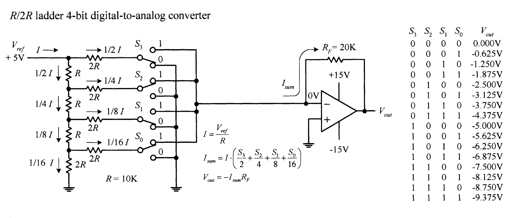
FIGURE 12.118
The trick to understanding how the R/2R ladder works is realizing that the current drawn through any one switch is always the same, no matter if it is thrown up or down. If a switch is thrown down, current will flow through the switch into ground (0 V). If a switch is thrown up, current will flow toward virtual ground—located at the op amp's inverting input (recall that if the noninverting input of an op amp is set to 0 V, the op amp will make the inverting input 0 V, via negative feedback). Once you realize that the current through any given switch is always constant, you can figure that the total current (I) supplied by Vref will be constant as well. Once you have that, you figure out what fractions of the total current pass through each of the branches within the R/2R network using simple circuit analysis. Figure 12.118 shows that ½I passes through S3 (MSB switch), ¼I through S2, ⅛I through S1, and 1⁄16I through S0 (LSB switch). If you're interested in how that was figured out, the circuit reduction shown in Fig. 12.119 should help.
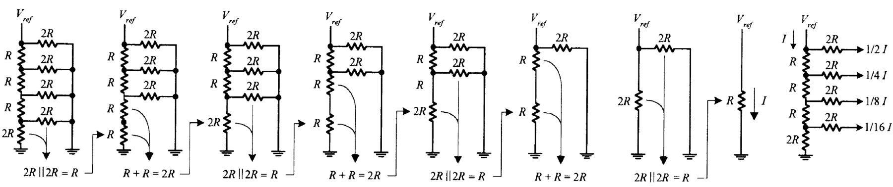
FIGURE 12.119
Now that we have a means of consistently generating fractions of 1⁄2I, 1⁄4I, 1⁄8I, and 1⁄16I, we can choose, via the digital input switches, which fractions are summed together by the amplifier. For example, if switches S3, S2, S1, and S0 are thrown to 0101 (5), 1⁄4 I + 1⁄16 I combine to form Isum. But what is I? Using Ohm's law, it's just I = Vref / R = +5 V / 10 kΩ = 500 µA. This means that Isum = 1⁄4(500 µA) + 1⁄16(500 µA) = 156.25 µA. The final output voltage is determined by Vout = -IsumRF = - (156.25 µA)(20 kΩ) = -3.125 V. The formulas and the table in Fig. 12.118 show the other possible binary/analog combinations.
To create an R/2R DAC with higher resolution, we simply add more runs and switches to the ladder.
Integrated DACs
Often, making DACs from scratch isn't worth the effort. The cost as well as the likelihood for conversion errors is great. The best thing to do is to simply buy a DAC IC. You can buy these devices from a number of different manufacturers (such as National Semiconductor, Analog Devices, and Texas Instruments). The typical resolutions for these ICs are 6, 8, 10, 12, 16, and 18 bits. DAC ICs also may come with a serial digital input, as opposed to the parallel input scheme shown in Figs 12.117 and 12.118. Before a serial-input DAC can make a conversion, the entire digital word must be clocked into an internal shift register.
Most often, DAC ICs come with an external reference input that is used to set the analog output range. There are some DACs that have fixed references, but these are becoming rare.
Often, you'll see a manufacturer list one of its DACs as being a multiplying DAC. A multiplying DAC can produce an output signal that is proportional to the product of a varying input reference level (voltage or current) times a digital code. As it turns out, most DACs, even those that are specifically designated as multiplying DAC on the data sheets, can be used for multiplying purposes simply by using the reference input as the analog input. However, many such ICs do not provide the same quality multiplying characteristics, such as a wide analog input range and fast conversion times, as those that are called multiplying DACs.
Multiplying is most commonly applied in systems that use ratiometeric transducers (for example, position potentiometers, strain gauges, and pressure transducers). These transducers require an external analog voltage to act as a reference level on which to base analog output responses. If this reference level is altered, say, by an unwanted supply surge, the transducer's output will change in response, and this results in conversion errors at the DAC end. However, if we use a multiplying DAC, we eliminate these errors by feeding the transducer's reference voltage to the DAC's analog input. If any supply voltage/current errors occur, the DAC will alter its output in proportion to the analog error.
DACs are capable of producing unipolar (single-polarity output) or bipolar (positive and negative) output signals. In most cases, when a DAC is used in unipolar mode, the digital code is expressed in standard binary. When used in bipolar mode, the most common code is either offset binary or 2's complement. Offset binary and 2's complement codes make it possible to express both positive and negative values. Figure 12.120 shows all three codes and their corresponding analog output levels (referenced from an external voltage source).
Common Digital Codes Used by DACs
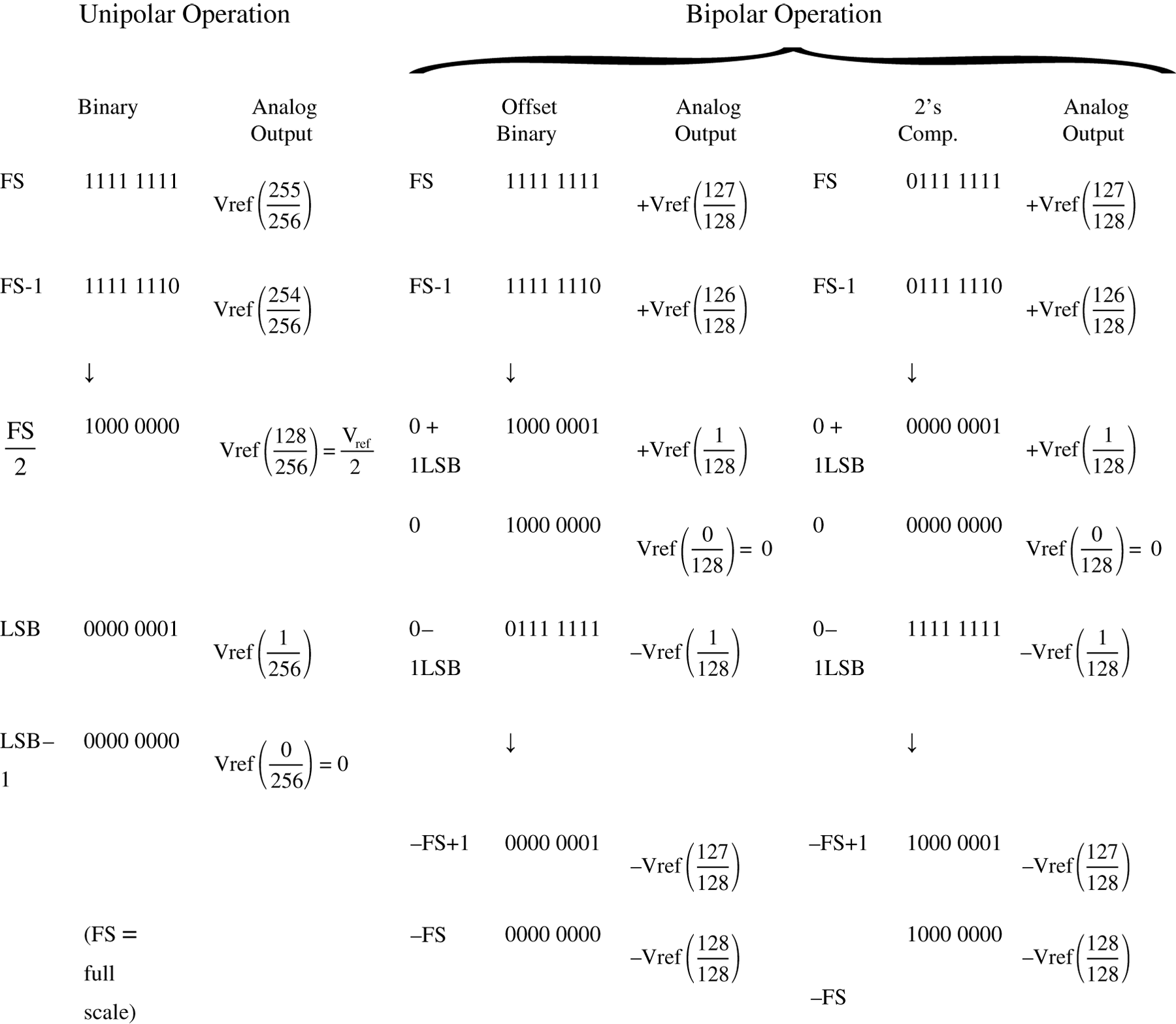
FIGURE 12.120
Note that in the figure, FS stands for full scale, which is the maximum analog level that can be reached when applying the highest binary code. It is important to realize that at full scale, the analog output for an n-bit converter is actually (2n - 1) / 2n × Vref, not 2n/2n × Vref. For example, for an 8-bit converter, the number of binary numbers is 28 = 256, while the maximum analog output level is 255/256 Vref, not 256/256 Vref, since the highest binary number is 255 (1111 1111). The "missing count" is used up by the LSB-1 condition (0 state).
Example DAC ICs
DAC0808 8-BIT DAC
The DAC0808 (National Semiconductor) is a popular 8-bit DAC that requires an input reference current and supplies 1 of 256 analog output current levels. Figure 12.121 shows a block diagram of the DAC0808, along with its IC pin configuration and a sample application circuit.
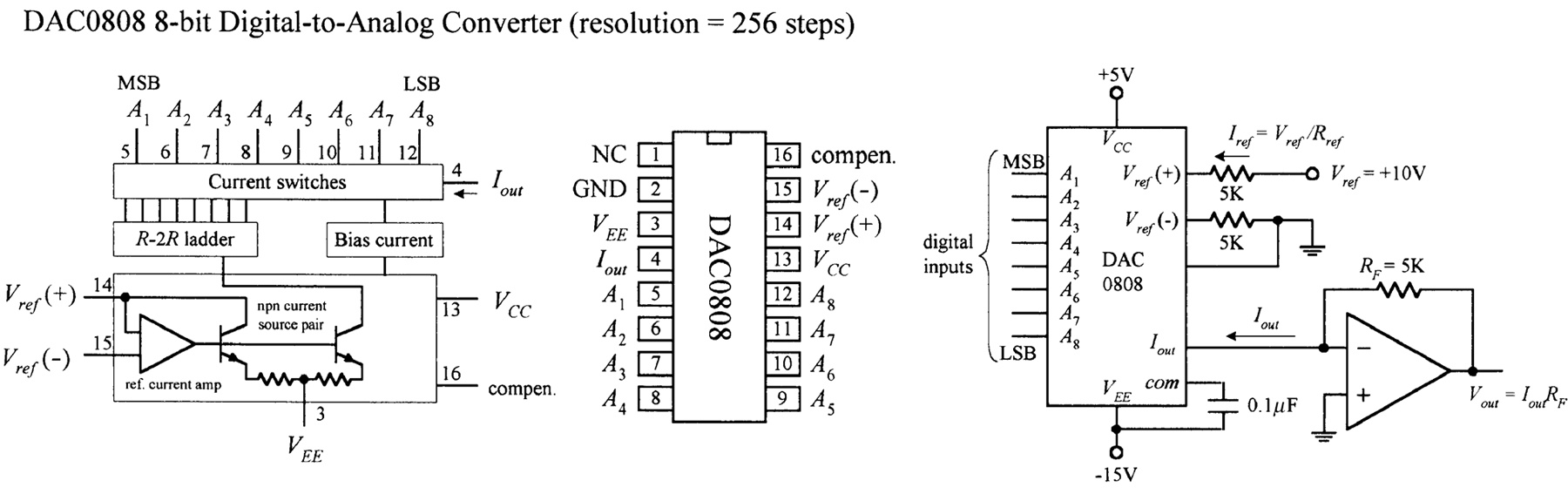
FIGURE 12.121
In the application circuit, the analog output range is set by applying a reference current (Iref) to pin 14 (+Vref). In this example, Iref is set to 2 mA via an external +10 V/5 kΩ resistor combination. Note that another 5-kΩ resistor is required between pin 15 (-Vref) and ground.
To determine the DAC's analog output current (Iout) for all possible binary inputs, we use the following formula:


At full scale (all A's high or binary 255), Iout = Iref (255/256) = (2 mA)(0.996) = 1.99 mA. Considering that the DAC has 256 analog output levels, we can figure that each corresponding level is spaced 1.99 mA/256 = 0.0078 mA apart.
To convert the analog output currents into analog output voltages, we attach the op amp. Using the op amp rules from Chap. 8, we find that the output voltage is Vout = Iout × Rf. At full scale, Vout = (1.99 mA)(5 kΩ) = 9.95 V. Each analog output level is spaced 9.95 V/256 = 0.0389 V apart.
The DAC0808 can be configured as a multiplying DAC by applying the analog input signal to the reference input. In this case, however, the analog input current should be limited to a range from 16 µA to 4 mA to retain reasonable accuracy. See the National Semiconductor's data sheets for more details.
DAC8043A SERIAL 12-BIT INPUT MULTIPLYING DAC
The DAC8083A (Analog Devices) is a high-precision 12-bit CMOS multiplying DAC that comes with a serial digital input. Figure 12.122 shows a block diagram, pin configuration, and write cycle timing diagram for this device.
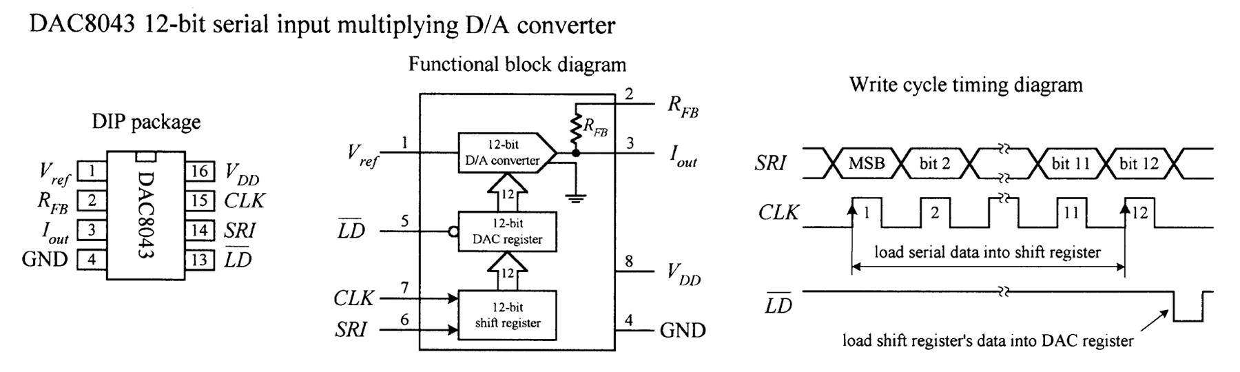
FIGURE 12.122
Before the DAC8043 can make a conversion, serial data must be clocked into the input register by supplying an external clock signal (each positive edge of the clock load one bit). Once loaded, the input register's contents are dumped off to the DAC register by applying a low pulse to the 
![]() line. Data in the DAC register is then converted to an output current through the Iout terminal.
line. Data in the DAC register is then converted to an output current through the Iout terminal.
In most applications, this current is then transformed into a voltage by an op amp stage, as is the case within the two circuits shown in Fig. 12.123. In the unipolar (two-quadrant) circuit, a standard binary code is used to select from 4096 possible analog output levels. In the bipolar (four-quadrant) circuit, an offset binary code is used again to select from 4096 analog output levels, but now the range is broken up to accommodate both positive and negative polarities.
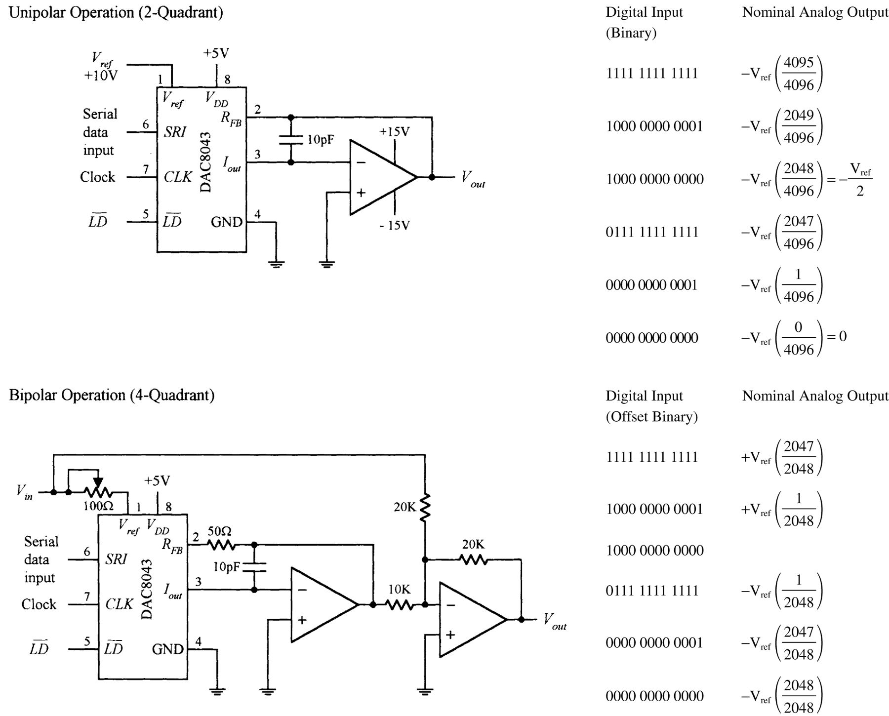
FIGURE 12.123
If you're interested in learning more about the DAC8043, go to Analog Device's website and check out the data sheet.
Another very similar device worth considering is the MAX522.
12.9.6 Analog-to-Digital Converters
There are a number of techniques used to convert analog signals into digital signals. The most popular techniques include successive approximation conversion and parallel-encoded conversion (or flash conversion). Other techniques include half-flash conversion, delta-sigma processing, and pulse-code modulation (PCM). In this section, we'll focus on the successive approximation and parallel-encoded conversion techniques. Most microcontrollers will have built-in ADC channels using one of the techniques described here.
Successive Approximation
Successive approximation analog-to-digital conversion is the most common approach used in integrated ADCs. In this conversion technique, each bit of the binary output is found, one bit at a time—MSB first. This technique yields fairly fast conversion times (from around 10 to 300 µs) with a limited amount of circuitry. Figure 12.124 shows a simple 8-bit successive approximation ADC, along with an example analog-to-digital conversion sequence.
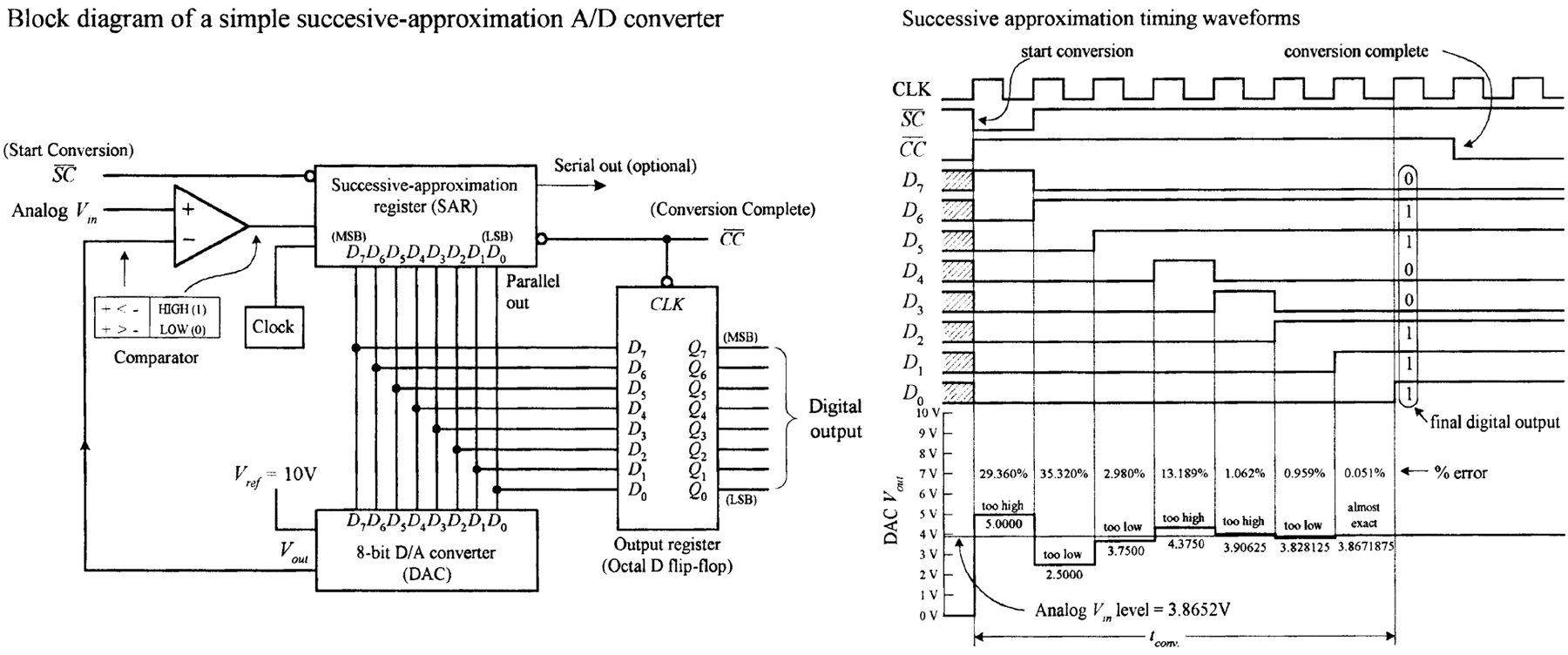
FIGURE 12.124
To begin a conversion, the 
![]() (start conversion) input is pulsed low. This causes the successive approximation register (SAR) to first apply a high on the MSB (D7) line of the DAC. With only D7 high, the DAC's output is driven to one-half its full-scale level, which in this case is +5 V because the full-scale output is +10 V. The +5-V output level from the DAC is then compared with the analog input level, via the comparator. If the analog input level is greater than +5 V, the SAR keeps the D7 line high; otherwise, the SAR returns the D7 line low. At the next clock pulse, the next bit (D6) is tried. Again, if the analog input level is larger than the DAC's output level, D6 is left high; otherwise, it is returned low.
(start conversion) input is pulsed low. This causes the successive approximation register (SAR) to first apply a high on the MSB (D7) line of the DAC. With only D7 high, the DAC's output is driven to one-half its full-scale level, which in this case is +5 V because the full-scale output is +10 V. The +5-V output level from the DAC is then compared with the analog input level, via the comparator. If the analog input level is greater than +5 V, the SAR keeps the D7 line high; otherwise, the SAR returns the D7 line low. At the next clock pulse, the next bit (D6) is tried. Again, if the analog input level is larger than the DAC's output level, D6 is left high; otherwise, it is returned low.
During the next six clock pulses, the rest of the bits are tried. After the last bit (LSB) is tried, the CC (conversion complete) output of the SAR goes low, indicating that a valid 8-bit conversion is complete, and the binary data is ready to be clocked into the octal flip-flop, where it can be presented to the Q0–Q7 outputs.
The timing diagram shows a 3.8652-V analog level being converted into an approximate digital equivalent. Note that after the first approximation (the D7 try), the percentage error between the actual analog level and corresponding digital equivalent is 29.360 percent. However, after the final approximation, the percentage error is reduced to only 0.051 percent.
Until now, we've assumed that the analog input to our ADC was constant during the conversion. But what happens when the analog input changes during conversion time? Errors result. The more rapidly the analog input changes during the conversion time, the more pronounced the errors will become. To prevent such errors, a sample-and-hold circuit is often attached to the analog input. With an external control signal, this circuit can be made to sample the analog input voltage and hold the sample while the ADC makes the conversion.
With the exception of very high-speed ADCs, separate ADC ICs are now largely redundant and have been replaced with microcontrollers containing 12-bit or higher ADC channels.
Parallel-Encoded Analog-to-Digital Conversion (Flash Conversion)
Parallel-encoded analog-to-digital conversion, or flash conversion, is perhaps the easiest conversion process to understand. To illustrate the basics behind parallel encoding (also referred to as simultaneous multiple comparator or flash converting), let's take a look at the simple 3-bit converter in Fig. 12.125.
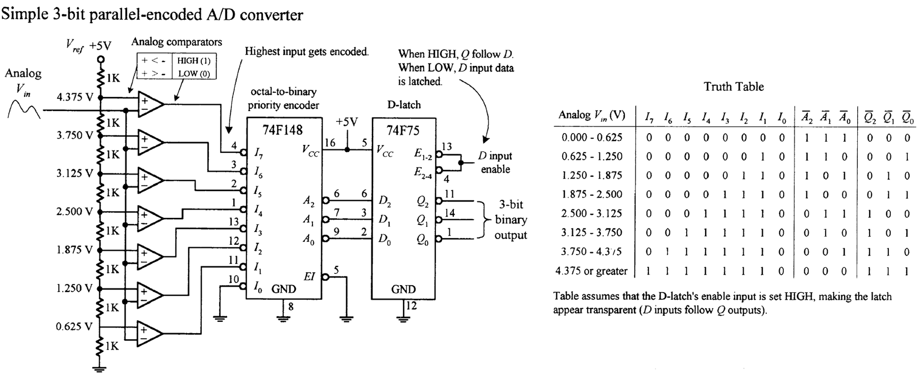
FIGURE 12.125
The set of comparators is the key feature to note in this circuit. Each comparator is supplied with a different reference voltage from the 1 kΩ voltage divider network. Since we've set up a +5V reference voltage, the voltage drop across each resistor within the voltage divider network is 0.625 V. From this, you can determine the specific reference voltages given to each comparator (see Fig. 12.125).
To convert an analog signal into a digital number, the analog signal is applied to all the comparators at the same time, via the common line attached to the inverting inputs of all the comparators. If the analog voltage is between, say, 2.500 and 3.125 V, only those comparators with reference voltage below 2.500 V will output a high. To create a 3-bit binary output, the eight comparator outputs are fed into an octal-to-binary priority encoder. A D latch also can be incorporated into the circuit to provide enable control of the binary output. The truth table should fill in the rest.
12.10 Displays
A number of displays can be interfaced with control logic to display numbers, letters, special characters, and graphics. Two popular displays that we'll consider here include the light-emitting diode (LED) display and the liquid-crystal display (LCD).
12.10.1 LED Displays
LED displays come in three basic configurations: numeric (numbers), alphanumeric (numbers and letters), and dot-matrix forms (see Fig. 12.126). Numeric displays consist of seven LED segments. Each LED segment is given a letter designation, as shown in the figure. Seven-segment LED displays are most frequently used to generate numbers (0–9), but they also can be used to display hexadecimal (0–9, A, B, C, D, E, F). The 14-segment, 16-segment, and special 4 × 7 dot matrix displays are alphanumeric. The 5 × 7 dot matrix display is both alphanumeric and graphic—you can display unique characters and simple graphics. See Chap. 5 for information about other types of LED displays.
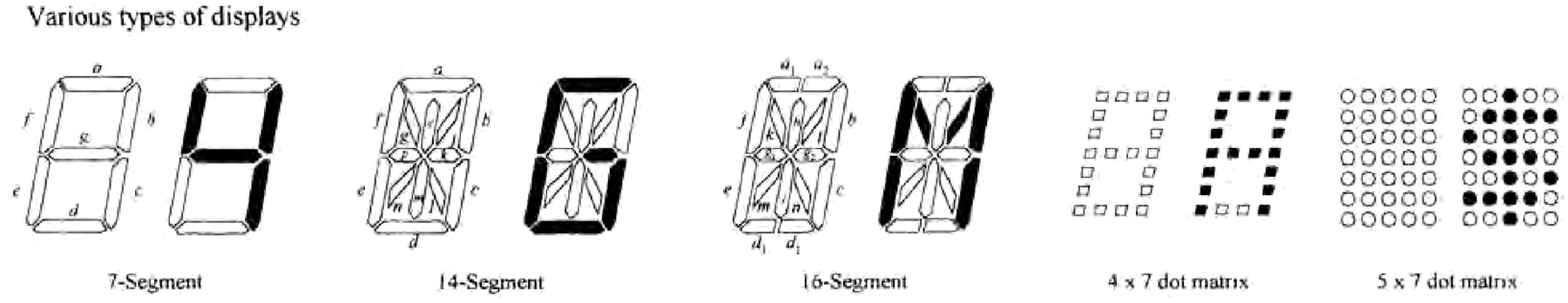
FIGURE 12.126
Direct Drive of Numeric LED Displays
Seven-segment LED displays come in two varieties: common anode and common cathode. Figure 12.128 shows single digital eight-segment (seven digit segments + decimal point) displays of both varieties.
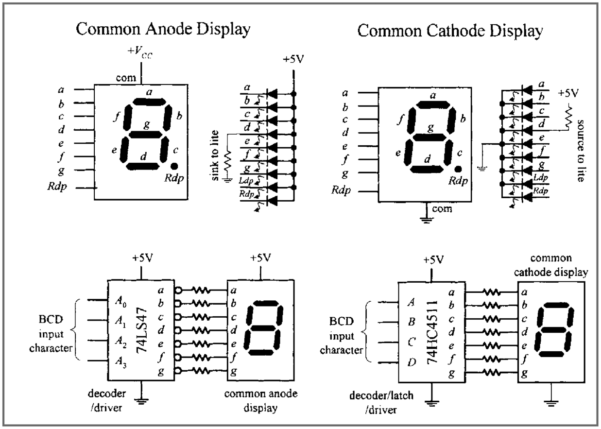
FIGURE 12.127
To drive a given segment of a common anode display, current must be sunk out through the corresponding segment's terminal. With the common cathode display, current must be sourced into the corresponding segment's terminal. A simple way to drive these displays is to use BCD to seven-segment display decoder/drivers, like the ones show in the figure. Applying a BCD input character results in a decimal digit being displayed (e.g., 0101 applied to A0–A3, or A–D displays a "5"). The 74LS47 active-low open-collector outputs are suited for a common anode display, while the 74HC4511's active-high outputs are suited for a common cathode display. Both ICs also come with extra terminals used for lamp testing and ripple blanking, as well as leading zero suppression (controlling the decimal point).
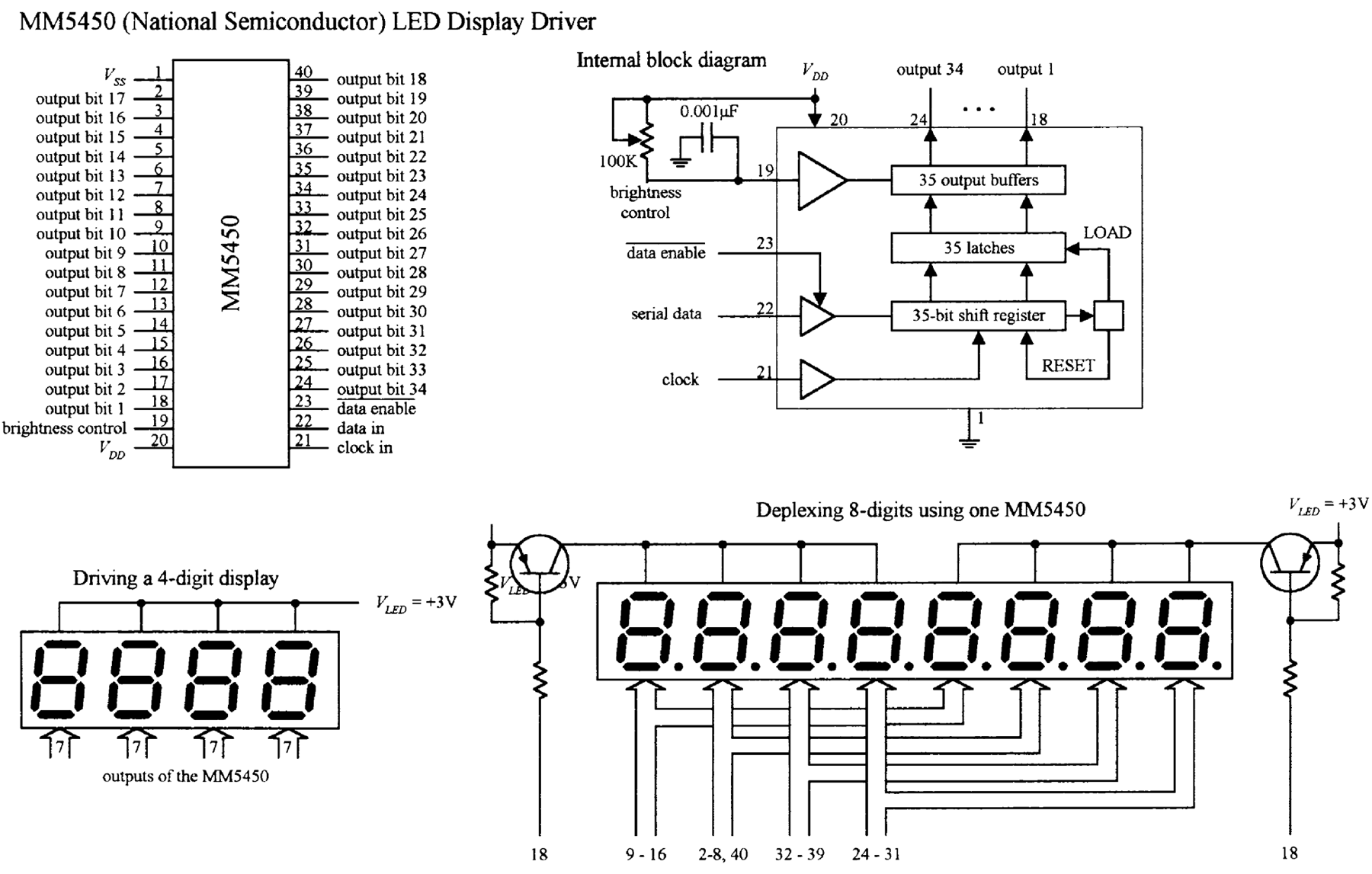
FIGURE 12.128
When driving a multidigit display, say, one with eight digits, the previous technique becomes awkward. It requires eight discrete decoder/driver ICs. One way to avoid this problem is to use a special direct-drive LED display driver IC.
For example, National Semiconductor's MM5450, shown in Fig. 12.133, is designed to drive 4- or 5-digit alphanumeric common anode LED displays. It comes with 34 TTL-compatible outputs that are used to drive desired LED segments within a display. Each of these outputs can sink up to 15 mA. In order to specify which output lines are driven high or low, serial input data are clocked into the driver's serial input. The serial data chain that is entered is 36 bits long. The first bit is a start bit (set to 1), and the remaining 35 bits are data bits. Each data bit corresponds to a given output data line that is used to drive a given LED segment within the display. At the thirty-sixth positive clock signal, a LOAD signal is generated that loads the 35 data bits into the latches (see the block diagram in Fig. 12.133). At the low state of the clock, a 
![]() signal is generated that clears the shift register for the next set of data. You can learn more about the MM5450 at http://www.micrel.com/_PDF/mm5450.pdf.
signal is generated that clears the shift register for the next set of data. You can learn more about the MM5450 at http://www.micrel.com/_PDF/mm5450.pdf.
Multiplexed LED Displays
Another technique used to drive multidigit LED displays involves multiplexing. Multiplexing can drastically reduce the number of connections needed between display and control logic. In a multiplexed display, digits share common segment lines. Also, only one digit within the display is lighted at a time. To make it appear that a complete readout is displayed, all the digits must be flashed very rapidly in sequence, over and over again. The simple example in Fig. 12.129 shows multiplexing in action.To reduce the component count further, you can do away with the 74HC4511 and just use 7 digital outputs from the microcontroller.
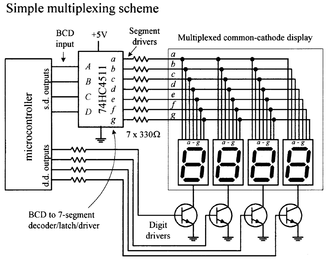
FIGURE 12.129
Here, we have a multiplexed common-cathode display—all digits share common segment lines (a–g). To supply a full one-digit readout, digits must be flashed rapidly, one at a time. To enable a given digit, the digit's common line is grounded via one of the digital drivers (transistors)—all other digits' common lines are left floating. In this example, the drivers are controlled by a microcontroller. To light the segments of a given digit, the microcontroller supplies the appropriate 4-bit BCD code to the seven-segment decoder/driver (74HC4511). As an example, if we wanted to display 1234, we would need to program the microcontroller (using software) to turn off all digits except the MSD (leftmost digit) and then supply the decoder/driver with the BCD code for 1. Then the next significant digit (2) would be driven, and then the next significant digit (3), and then the LSD (4). After that, the process would recycle for as long as we wanted our program to display 1234.
12.10.2 Liquid-Crystal Displays
In low-power CMOS digital systems (for example, battery- or solar-powered electronic devices), the dissipation of an LED display can consume most of a system's power requirements, which is something you want to avoid, especially since you are looking to save power when using CMOSs. LCDs, on the other hand, are ideal for low-power applications.
Unlike an LED display, an LCD is a passive device. This means that instead of using electric current to generate light, it uses light that is already externally present (such as sunlight, room lighting). For the LCD's optical effects to occur, the external light source needs to supply only a minute amount of power (within the mW/cm2 range).
Simple Alphanumeric Display
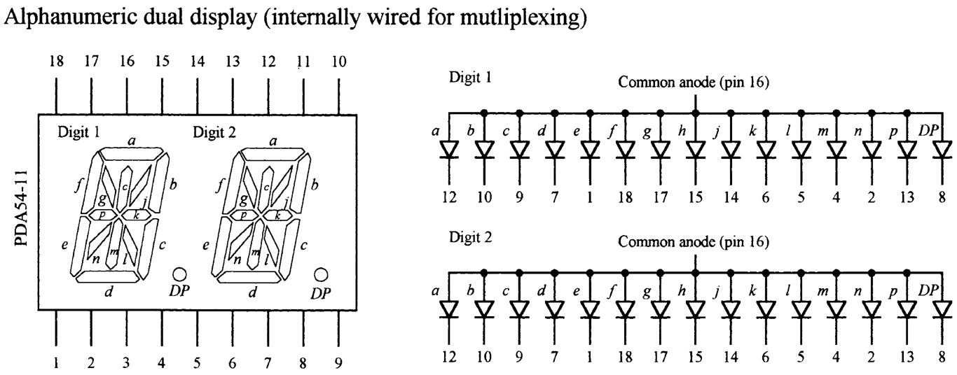
FIGURE 12.130
Figure 12.130 shows a common anode, 2-character, 14-segment (+ decimal) alphanumeric display. Notice that the segments of the two characters are internally wired together. This means that the display is designed for multiplexing. Though it is possible to use a microcontroller along with transistor drivers to control this display, the number of lines required is fairly large. Another option is to use a special driver IC, like Intersil's ICM7243B 14-segment 6-bit ASCII driver. Another alternative is simply to avoid using this kind of display and use a "smart" alphanumeric display that contains all the necessary control logic (drivers, code converters, and so on).
"Smart" Alphanumeric Display
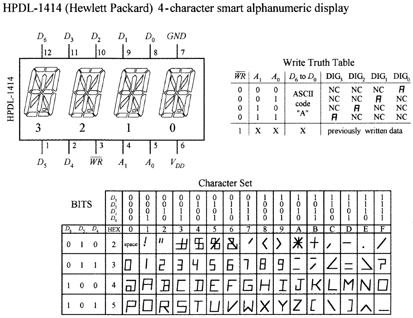
FIGURE 12.131
The HPDL-1414 is a "smart," 4-character, 16-segment display. This device is complete with LEDs, on-board 4-word ASCII memory, a 64-word character generator, 17-segment drivers, 4-digit drivers, and scanning circuitry necessary to multiplex the four LED characters. It is TTL-compatible and relatively easy to use. The seven data inputs D0 to D6 accept a 7-bit ASCII code, while the digital select inputs A0 and A1 accept a 2-bit binary code that is used to specify which of the four digits is to be lighted. The WRITE 
 input is used to load new data into memory. After a character has been written to memory, the IC decodes the ASCII data, drives the display, and refreshes it without the need for external hardware or software.
One disadvantage with LCDs is their slow switching speeds (the time it takes for a new digit/character to appear). Typical switching speeds for LCDs range from around 40 to 100 ms. At low temperatures, the switching speeds get even worse. Another problem with LCDs is the requirement that external light be present. Though there are LCD displays that come with backlighting (such as an LED behind the display), obviously, this will increase power consumption.
Basic Explanation of How an LCD Works
An LCD consists of a number of layers that include a polarizer, a set of transparent electrodes, a liquid-crystal element, a transparent back electrode, a second polarizer, and a mirror (see the leftmost illustration in Fig. 12.132).
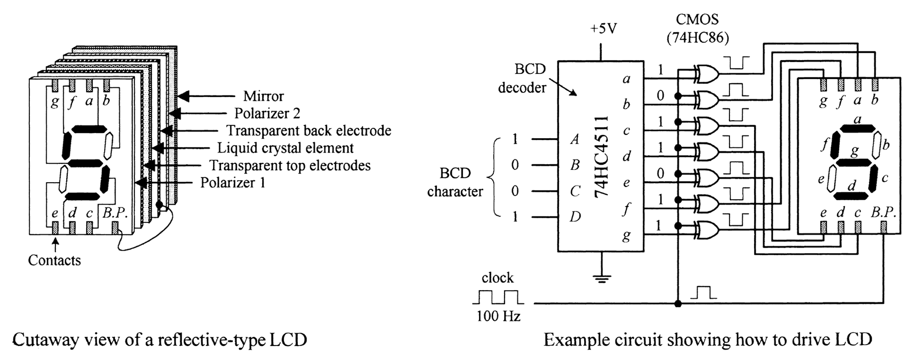
FIGURE 12.132
The transparent top electrodes are used to generate the individual segments of a digit, character, and so on, while the transparent back electrode forms a common plane, often referred to as the back plane (BP). The top electrode segments and the back electrode are wired to external contacts. With no potential difference between a given top electrode and the back electrode, the region where the top electrode is located appears silver in color against a silver background. However, when a potential is applied between a given top electrode and back electrode, the region where the top electrode is located appears dark against a silver background.
The circuit in Fig. 12.132 shows a basic way to drive a seven-segment LCD. It uses a 74HC4511 BCD decoder and XOR gates to generate the prior drive signals for the LCD. A very important thing to note in this circuit is the clock. As it turns out, an LCD actually requires ac drive signals (for example, squarewaves) instead of dc drive signals. If dc were used, the primary component of the display—namely, the liquid crystal—would undergo electrochemical degradation (more on the liquid crystal in a moment). The optimal frequency of the applied ac drive signal is typically from around 25 Hz to a couple hundred hertz. Now that we understand that, it is easy to see why we need the XOR gates.
As the clock delivers squarewaves to the back electrode (back plane, or BP), the XOR gates act as enable gates that pass and invert a signal and apply it to a given top electrode segment. For example, if a BCD code of 1001 (5) is applied to the decoder, the decoder's outputs a, c, d, f, and g go high, while outputs b and e go low. When a positive clock pulse arrives, XOR gates attached to the outputs that are high invert the high levels. XOR gates attached to outputs that are low pass on the low levels. During the same pulse duration, the back plane is set high. Potentials now are present between a, c, d, f, and g segments and the back plane, and therefore these segments appear dark. Segments b and e, along with the background, appear silverish because no potential exists between them and the back plane. Now, when the clock pulse goes low, the display remains the same (provided the BCD input hasn't changed), since all that has occurred is a reverse in polarity. This has no effect on the optical properties of the display.
Detailed Explanation of How an LCD Works (the Physics)
Figure 12.133 shows how an LCD generates a clear (silverish) segment. When control signals sent to the transparent top and back electrodes are in phase, no potential exists between the two electrodes. With no potential present, the cigar-shaped organic liquid crystals (nematic crystals) arrange themselves in spiral state, as shown in the figure.
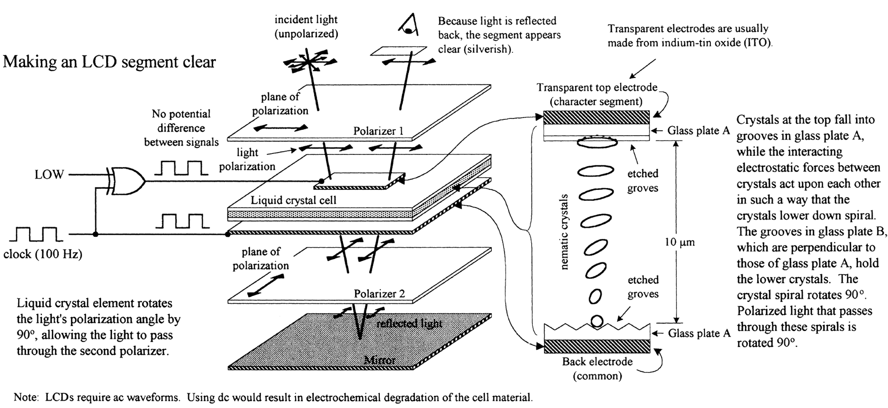
FIGURE 12.133
The upper crystal aligns itself horizontal to the page, while the lowest crystal aligns itself perpendicular to the page. The upper crystal and the lower crystal are held in place by tiny grooves that are etched into the inner surfaces of the glass surfaces of the cell. Crystals in between the upper crystal and the lower crystal progressively spiral 90° due to electrostatic forces that exist between neighboring crystals. When polarized light passes through a region of the display that contains these spirals, the polarization angle of the light is rotated 90°.
Now, looking at the display as a whole, when incident unpolarized light passes through polarizer 1 (as shown in the figure), the light becomes polarized in the same direction of the plane of polarization of the first polarizer. The polarized light then passes through the transparent top electrode and enters the liquid-crystal cell. As it passes through the cell, its polarization angle is rotated 90°. The polarized light that exits the cell then passes through the transparent back electrode and the second polarizer without problems. (If we were to remove the liquid-crystal cell, all polarized light that passed through the first polarizer would be absorbed, since we would have crossed polarizers.) The light that passes through the second polarizer then reflects off the mirror, passes through the second polarizer, on through the liquid-crystal cell (getting rotated 90°), through the first polarizer, and finally reaches the observer's eye. This reflected light appears silver in color. Note that the background of LCDs constantly appears silver because no potential exists across the liquid-crystal cell in the background region.
Figure 12.134 shows how an LCD generates a dark segment. When control signals sent to the top and back electrodes are out of phase, a potential difference exists between the two electrodes. This causes the crystals to align themselves in a parallel manner, as shown in the figure. When the polarized light from the first polarizer passes through the cell region containing these parallel crystals, nothing happens—the polarization angle stays the same. However, when the light comes in contact with the second polarizer, it is absorbed because the angle of polarization of the light and the plane of polarization of the second polarizer are perpendicular to each other. Since light reaches the mirror, no light is reflected back to the observer's eye, and hence the segment appears dark.
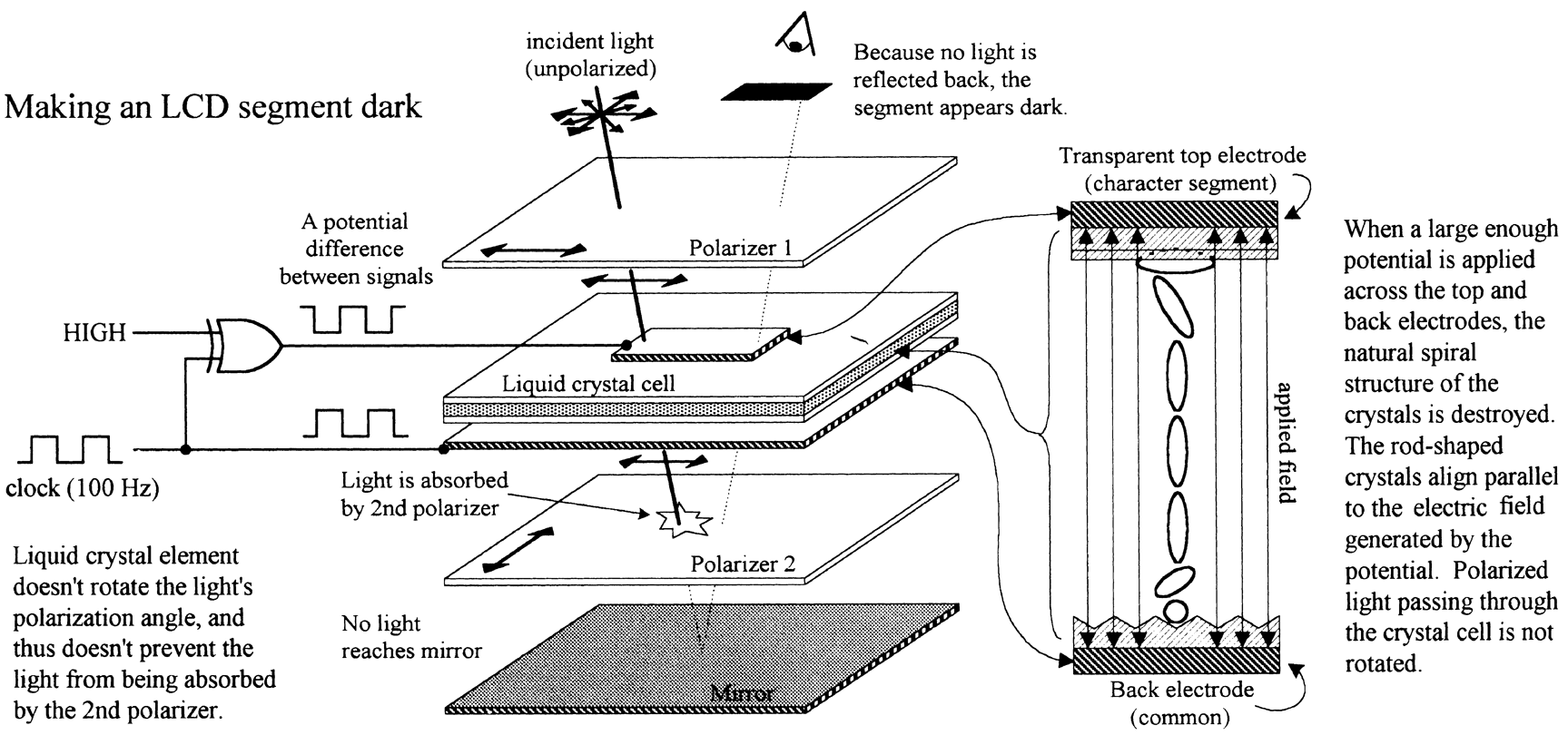
FIGURE 12.134
The LCD shown in Fig. 12.133 represents what is referred to as a standard twisted nematic display. Another common LCD is the supertwist nematic display. Unlike the standard twisted display, this display's nematic crystals rotate 270° from top to bottom. The extra 180° twist improves the contrast and viewing angle.
Driving LCDs
CD4543B CMOS BCD-TO-SEVEN-SEGMENT LATCH/DECODER/DRIVER
The CD4543B (Texas Instruments), shown in Fig. 12.135, is a BCD-to-seven-segment latch/decoder/driver that is designed for LCDs, as well as for LED displays. When used to drive LCDs, a squarewave must be applied simultaneously to the CD4543B's Phase (Ph) input and to the LCD's back plane. When used to drive LED displays, a high is required at the Phase input for common cathode displays, while a low is required for common anode displays. To blank the display (set outputs a–g low), the BL input is set high. The CD4543B also comes with a Latch Disable input (LD), which can be used to latch onto input data, preventing new input data from altering the display.
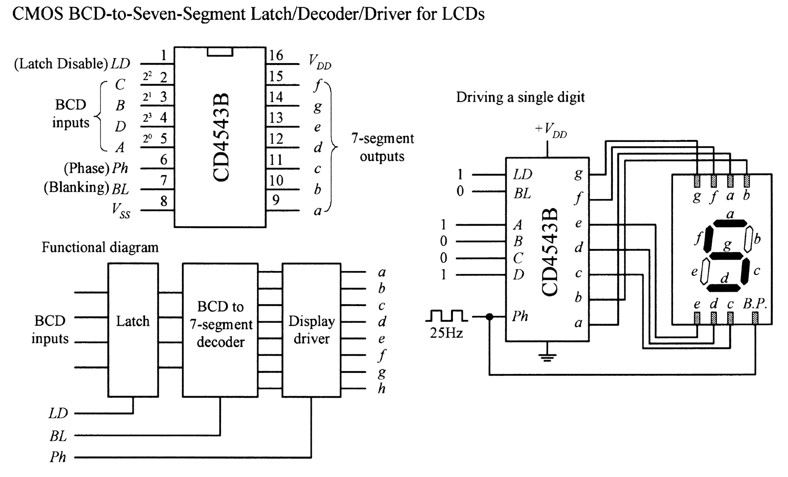
FIGURE 12.135
MM5453 LCD DRIVER
The MM5453 (National Semiconductor) is a 40-pin IC that can drive up to 33 segments of an LCD, which can be used to drive 4½-digit seven-segment displays. It houses an internal oscillator section (requiring an external RC circuit) that generates the necessary squarewaves used to drive the LCD. To activate given segments within the display, a serial code is applied to the data input. The code first starts out with a start bit (high) followed by data bits that specify which outputs should be driven high or low. Figure 12.136 shows an example display circuit, along with corresponding data format required to drive a 4½-digit display.
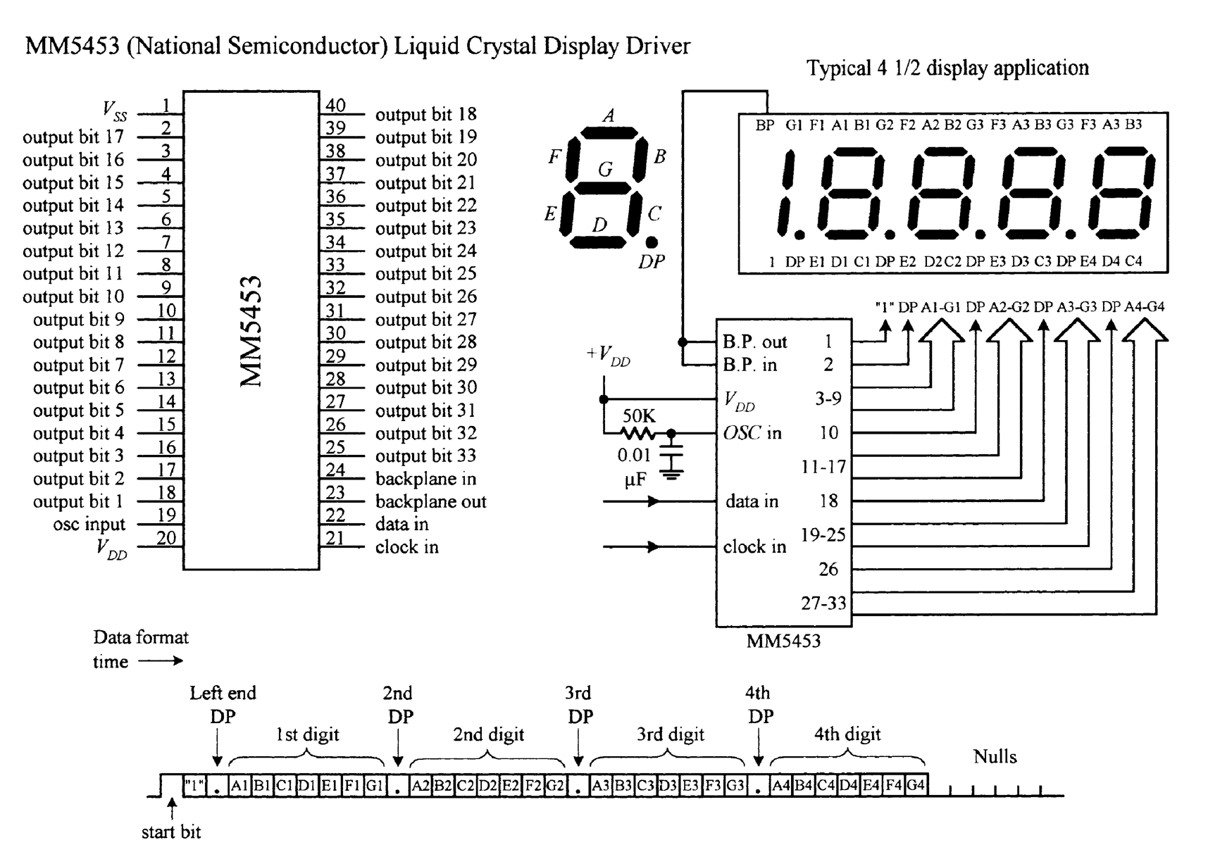
FIGURE 12.136
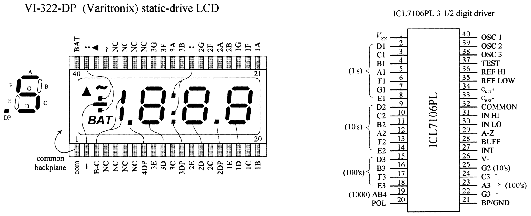
FIGURE 12.137
VI-322-DP LCD AND ICL7106 3½-DIGIT LCD, ADC DRIVER
There are a number of specialized LCDs that can be found in the electronics catalogs. An example is Varitronix's VI-322-DP 3½-digit (plus ∼, +, BAT, Δ) LCD, shown in Fig. 12.136. This display is configured in a static drive arrangement (each segment has a separate lead) and is found in many test instruments. To drive this display, you first check to see what kind of driver the manufacturer suggests. In this case, the manufacturer suggests using Intersil's ICL7106. This IC is a 3½-digit LCD/LED display driver as well as an ADC. This dual-purpose feature makes it easy to interface transducers directly to the same IC that is driving the display. To learn how to use the ICL7106, check out Intersil's data sheet at http://www.intersil.com.
Multiplexed LCDs
We have just seen examples of static-drive-type LCDs, where each segment (to electrode) had its own lead, and a single common plane was used as the back electrode. Another type of LCD is designed with multiplexing in mind and is referred to as dynamic drive or multiplexed display.
As with the multiplexed LED display, multiplexed LCDs can greatly reduce the number of external connections required between the display and driver. However, they require increased complexity in drive circuitry (or software) to drive. In a multiplexed LCD, appropriate segments are connected together to form groups that are sequentially addressed by means of multiple back-plane electrodes.
"Intelligent" Dot-Matrix LCD Modules
Dot-matrix LCDs are used to display alphanumeric characters and other symbols. These displays are used in cell phones, calculators, vending machines, and many other devices that provide the user with simple textual information. Dot-matrix LCDs are also used in laptop computer screens; however, these displays incorporate special filters, multicolor back lighting, and so on. For practical purposes, we'll concentrate on the simple alphanumeric LCDs.
An alphanumeric LCD screen is usually divided into a number of 5 × 8 pixel blocks, with vertical and horizontal spaces separating each block. Figure 12.138 shows a display with 20 columns and 4 rows of 5 × 8 pixel blocks. Other standard configurations come with 8, 16, 20, 24, 32, or 40 columns and 1, 2, or 4 rows. To generate a character within a given block requires that each pixel within the block be turned on or off. As you can imagine, to control so many different pixels (electrode segments) requires a great deal of sophistication. For this reason, an intelligent driver IC is required.
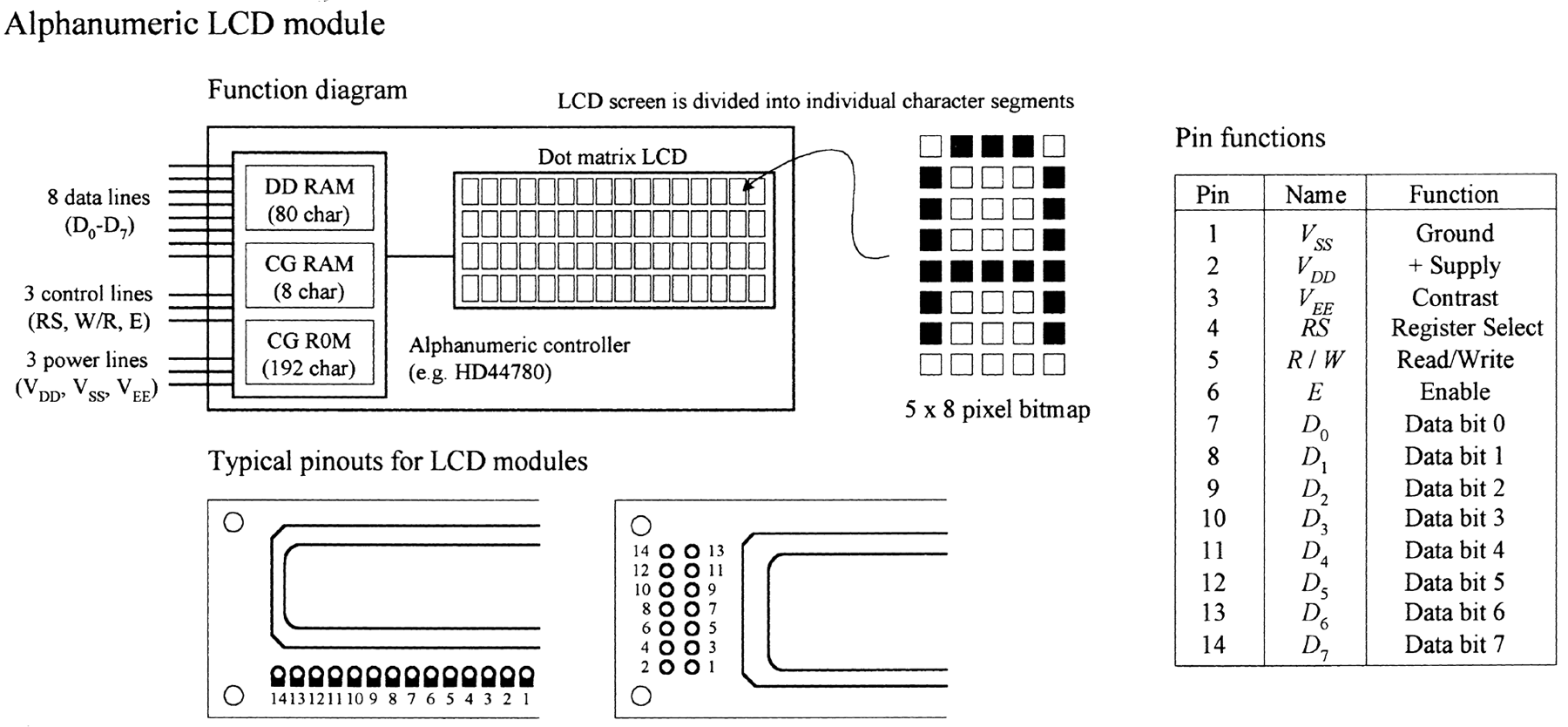
FIGURE 12.138
Almost all alphanumeric LCD modules are controlled by Hitachi's HD44780 (or equivalent) driver IC. This driver contains the following:
- A permanent memory (CG ROM) that stores 192 alphanumeric characters
- A random access memory (DD RAM) used to store the display's contents
- A second random access memory (CG RAM) used to hold custom symbols
- Input lines for data and instruction control signals
- Multiplexed outputs for driving LCD pixels
- Additional outputs for communicating with expansion chips to drive more LCD pixels
This driver is built right into the LCD module. (You could attempt to construct your own module by interfacing the driver with an LCD, but it would not be worth the effort—the numerous tiny connections would drive you nuts.) From now on, all modules described in this section are assumed to be HD44780-driven.
BASIC OVERVIEW OF THE PINS
The standard LCD module comes with a 14-pin interface: eight data lines (D0–D7), three control lines (RS, W/R, and E), and three power lines (VDD, VSS, and VEE).
VDD (pin 2) and VSS (pin 1) are the module's positive and negative power supply leads. Usually, VDD is set to +5 V, while VSS is grounded. VEE (pin 3) is the display's contrast control. By changing the voltage applied to this lead, the contrast of the display increases or decreases. A potentiometer placed between supply voltages, with its wiper connected to VEE, allows for manual adjustment.
D0–D7 (pins 7–14) are the data bus lines. Data can be transferred to and from the display either as a single 8-bit byte or as two 4-bit nibbles. In the latter case, only the upper four data lines (D4–D7) are used.
RS (pin 4) is the Register Select line. When this line is low, data bytes transferred to the display module are interpreted as commands, and data bytes read from the display module indicate its status. When the RS line is set high, character data can be transferred to and from the display module.
R/W (pin 5) is the Read/Write control line. To write commands or character data to the module, R/W is set low. To read character data or status information from the module, R/W is set high.
E (pin 6) is the Enable control input, which is used to initiate the actual transfer of command or character data to and from the module. When writing to the display, data on the D0–D7 lines is transferred to the display when the enable input receives a high-to-low transition. When reading from the display, data become available to the D0–D7 lines shortly after a low-to-high transition occurs at the enable input and will remain available until the signal goes low again.
Figure 12.139 shows the instruction set and standard set of characters for an LCD module. Next, we'll go through some examples illustrating how to use the instructions and how to write characters to the display.
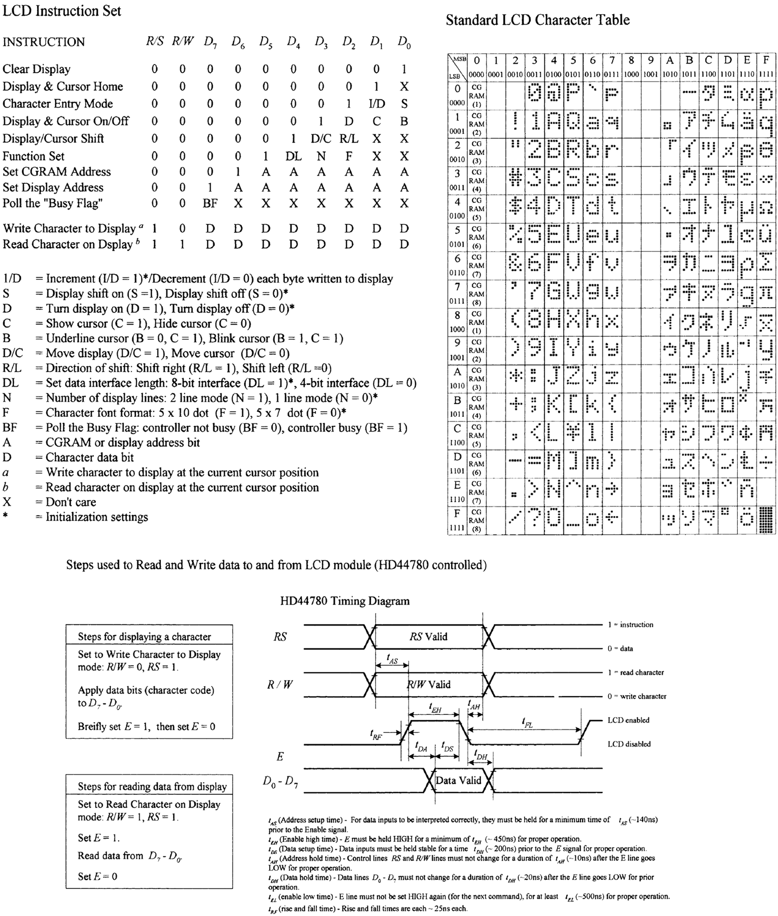
FIGURE 12.139
TEST CIRCUIT USED TO DEMONSTRATE HOW TO CONTROL THE LCD MODULE
Figure 12.140 shows a simple test circuit that is quite useful for learning how to send commands and character data to the LCD module. (In reality, the LCD module is connected to a microprocessor or microcontroller, as shown to the left in the figure.) In this circuit, switches connected to data inputs use pullup resistors in order to supply a high (1) when the switch is open or supply a low (0) when the switch is closed.
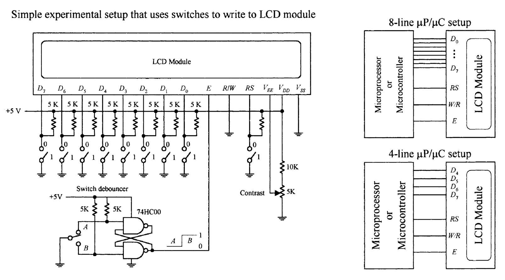
FIGURE 12.140
The enable input receives its high and low levels from a debounced toggle switch. Debouncing the enable switch prevents the likelihood of multiple enable signals being generated. Multiple enable signals tend to create unwanted effects, such as generating the same character over and over again across the display. The 5-kΩ pot is used for contrast. Note that in this circuit, we've grounded the R/W line, which means we'll only deal with writing to the display.
WHEN POWER IS FIRST APPLIED
When power is first applied to the display, the display module resets itself to its initial settings. Initial settings are indicated in the LCD instruction set with an asterisk. As indicated, the display is actually turned off during the initial setting condition. If we attempt to write character data to the display now, nothing will show up. In order to show something, we must issue a command to the module telling it to turn on its display.
According to the instruction set, the Display & Cursor On/Off instruction can be used to turn on the display. At the same time, this instruction also selects the cursor style. For example, if we apply the command code 0000 1111 to D7–D0, making sure to keep RS low so the module will interpret data as a command, a blinking cursor with an underline should appear at the top leftmost position on the display. But before this command can take effect, it must be sent to the module by momentarily setting the Enable (E) line low.
Another important instruction that should be implemented after power-up is the Function Set command. When a two-line display is used, this command tells the module to turn on the second line. It also tells the module what kind of data transfer is going to be used (8-bit or 4-bit), and whether a 5 × 10 or 5 × 7 pixel format will be used (5 × 10 is found in some one-line displays). Assuming that the display used in our example circuit is a two-line display, we can send the command 0011 1000 telling the display to turn on both lines, use an 8-bit transfer, and provide a 5 × 7 pixel character format. Again, to send this command, we set RS low, then supply the command data to D7–D0, and finally pulse E low.
Now that the module knows what format to use, we can try writing a character to the display. To do this, we set the module to character mode by setting RS high. Next, we apply one of the 8-bit codes listed in the standard LCD character set table to the data inputs D7–D0. For example, if we want to display the letter Q, we apply 01010001 (hex 51 or 51H). To send the character data to the LCD module, we pulse E low. A Q should then appear on the display. To clear the screen, we use the Clear Display command 0000 0001, remembering to keep RS low and then pulsing E low.
ADDRESSING
After power-up, the module's cursor is positioned at the far-left corner of the first line of the display. This display location is assigned a hexadecimal address of 00H. As new characters are entered, the cursor automatically moves to the right to a new address of 01H, then 02H, and so on. Although this automatic incrementing feature makes life easy when entering characters, there are times when it is necessary to set the cursor position to a location other than the first address location.
To set the cursor to another address location, a new starting address must be entered as a command. There are 128 different addresses to choose from, although not all these addresses have their own display location. In fact, there are only 80 display locations laid out on a single line in one-line mode or 40 display locations laid out on each line in two-line mode. Now, as it turns out, not all display locations are necessarily visible on the screen at one time. This will be made more apparent in a moment. Let's first try a simple address example with the LCD module set to two-line mode (provided that two lines are actually available).
To position the cursor to a desired location, we use the Set Address command. This command is specified with the binary code 1000 0000 + (binary value of desired hex address). For example, to send a command telling the cursor to jump to the 07H address location, we apply (1000 0000 + 0000 0111) = 1000 0111 to the D7–D0 inputs, remembering to hold RS low and then pulsing E low. The cursor should now be located at the eighth position over from the left.
It is important to realize that the relationship between addresses and display locations varies from module to module. Most displays are configured with two lines of characters, with the first line starting at address 00H and the second line at address 40H. Figure 12.141 shows the relationship between the address and display locations for various LCD modules. Note that the four-line module is really a two-line type with the two lines split, as shown in the figure.
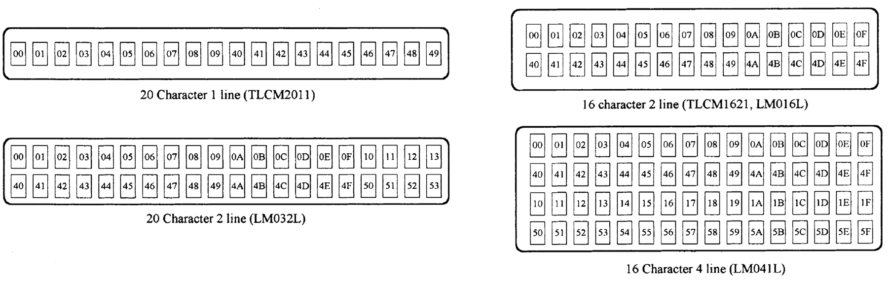
FIGURE 12.141
SHIFTING THE DISPLAY
Regardless of their size, LCD modules have 80 display locations that can be written to. With smaller displays, not all 80 locations can be displayed at once on the screen. For example, if we were to enter all the letters of the alphabet onto the first line of a 20-character display, only letters A through T would appear on the screen. Letters S through Z, along with the cursor, would be "pushed off" to the right of the screen, hidden from view.
To bring these hidden characters into view, we can apply the Cursor/Display Shift command to shift all display locations to the left. The command for shifting to the left is 0001 1000. Every time this command is issued, the characters shift one step to the left. In our example, it would take seven of these commands to bring T through Z and the cursor into view.
To shift things to the right, we apply the command 0001 1100. To bring the cursor back to address 00H and shift the display address 00H back to the left-hand side of the display, a Cursor Home command (0000 0010) can be issued. Another alternative is to use the Clear Display command 0000 0001. However, this command also clears all display locations.
CHARACTER ENTRY MODE
If you do not want to enter characters from left to right, you can use the Character Entry Mode command to enter characters from right to left. To do this, the cursor must first be sent to the rightmost display location on the screen. After that, the Character Entry Mode command 0000 0111 is entered into the module. This sets the entry mode to autoincrement/display shift left. Now, when characters are entered, they appear on the right-hand side, while the display shifts left for each character entered.
USER-DEFINED GRAPHICS
Commands 0100 0000 to 0111 1111 are used to program user-defined graphics. To program these graphics on-screen, the display is cleared, and the module is sent a Set Display Address command to position the cursor at address 00H. At this point, the contents of the eight user character locations can be viewed by entering binary data 0000 0000 to 0000 0111 in sequence. These characters will appear initially as garbage.
To start defining the user-defined graphics, a Set CGRAM command is sent to the module. Any value between 0100 0000 (40H) and 0111 1111 (7F) will work. Data entered from now on will be used to construct the user-defined graph, row by row. For example, to create a light bulb, the following data entries are made: 0000 1110, 0001 0001, 0001 0001, 0001 0001, 0000 1110, 0000 1010, 0000 1110, 0000 0100. Notice that the first three most significant bits are always 0 because there are only 5 pixels per row. Other user-defined graphics can be defined by entering the 8-byte sequence, and so on. Figure 12.142 shows how the CGRAM address corresponds to the individual pixels of the user-defined graphic.
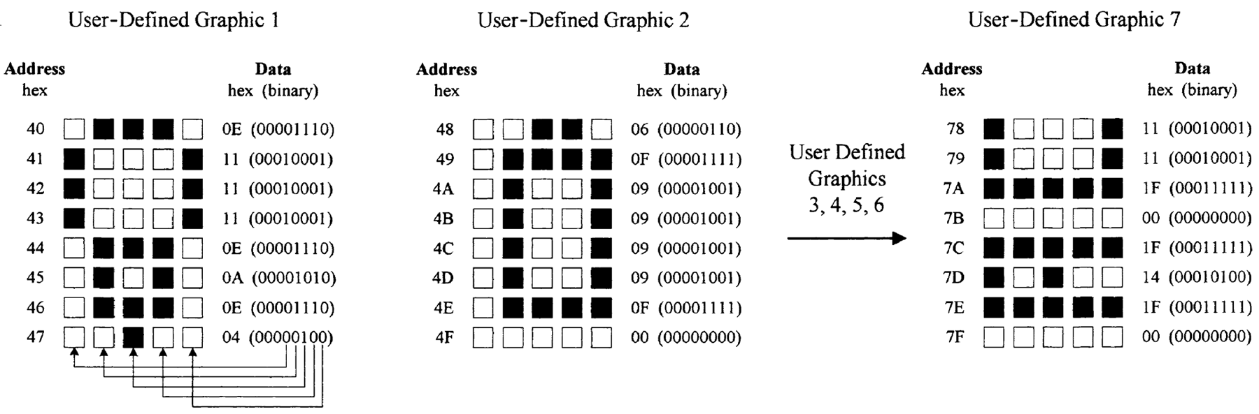
FIGURE 12.142
There are up to eight user-defined graphics that can be programmed. These then become part of the character set and can be displayed by using codes 0000 0000 to 0000 1111 or 0000 1000 to 0000 1111, both of which produce the same result.
One problem when creating user-defined graphics is they will be lost when power is removed from the module—a result of the volatile CGRAM. Typically, the user-defined graphic data is actually stored in an external nonvolatile EPROM or EEPROM, where the data is copied by a microprocessor and loaded into the display module sometime after power-up.
4-BIT DATA TRANSFER
As indicated in the Function Set command, the LCD module is capable of both 8-bit and 4-bit data transfer. In 4-bit mode, only data lines D4–D7 are used. The other four lines, D0–D3, are left either floating or tied to the power supply. To send data to the display requires sending two 4-bit chunks instead of one 8-bit word.
When power is first applied, the module is set up for 8-bit transfer. To set up 4-bit transfer, the Function Set command with binary value 0010 0000 is sent to the display. Note that since there are only four data lines in use, all 8 bits cannot be sent. However, this is not a problem, since the 8-bit/4-bit selection is on data bit D4. From now on, 8-bit character and command bits must be sent in two halves, the first 4 most significant bits and then the remaining 4 bits. For example, to write character data 0100 1110 to the display requires setting RS high, applying 0100 to the data lines, pulsing E low, then applying 1110 to the data lines, and pulsing E low again.
The 4-bit transfer is frequently used when the LCD module is interfaced with a microcontroller that has limited I/O lines. See Fig. 12.142.
12.11 Memory Devices
Memory devices provide a means of storing data on a temporary or permanent basis for future recall. The storage medium used in a memory device may be a semiconductor-based IC (primary memory), a magnetic tape, a magnetic disk, or an optical disk (secondary memories). In most cases, the secondary memories are capable of storing more data than primary memories because their surface areas are larger. However, secondary memories take much longer to access (read or write) data because memory locations on a disk or tape must be physically positioned to the point where they can be read or written to by the read/write mechanism. Within a primary memory device, memory locations are arranged in tiny regions within a large matrix, where each memory location can be accessed quickly (matter of nanoseconds) by applying the proper address signals to the rows within the matrix.
Figure 12.143 shows an overview of primary and secondary memories. In this section, we'll discuss only the primary memories, since these devices are used more frequently in designing gadgets than secondary memories. Secondary memories are almost exclusively used for storing large amounts of computer data, audio data, or video data.
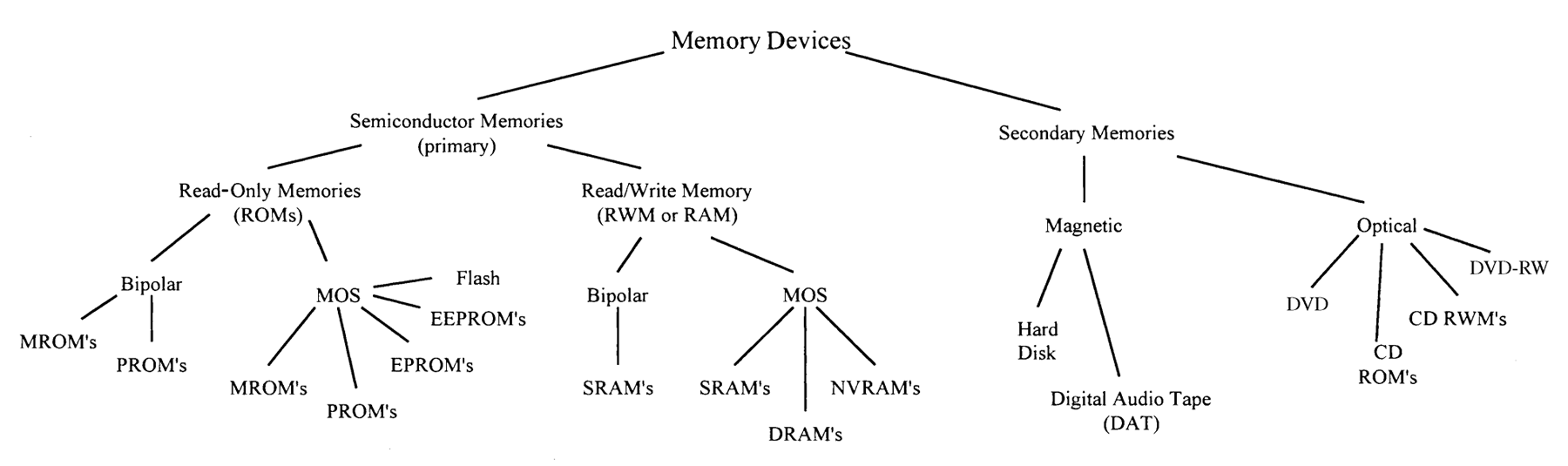
FIGURE 12.143
Today, the technology used in the construction of primary memory devices is almost exclusively based on MOSFET transistors. Bipolar transistors are also used within memory ICs. However, these devices are less popular because the amount of data they can store is significantly smaller than that of a memory IC built with MOSFET transistors. At one time, bipolar memories had a significant edge in speed over MOSFET memories, but today the speed gap has almost disappeared.
Memory devices consist of two basic subfamilies: read-only memory (ROM) and read/write memory (RWM), which is more commonly referred to as random-access memory (RAM). Within each of these subfamilies exist more subfamilies, as shown in Fig. 12.143. Let's start out by discussing the ROM devices.
12.11.1 Read-Only Memory
ROM is used to store data on a permanent basis. These devices are capable of random access, like RAM devices, but unlike RAM devices, they do not lose stored data when power is removed from the IC.
ROM is used in nearly all computers to store boot-up instructions (such as stack allocation, port and interrupt initializations, and instructions for retrieving the operating system from disk storage) that are enacted when the computer is first turned on.
In some microcontroller applications (simple-function gadgets, appliances, toys, and so on), the entire stand-alone program resides in ROM. The microcontroller's central processing unit (CPU) retrieves the program instructions and uses volatile RAM for temporary data storage as it runs through the ROM's stored instructions.
In some instances, you find ROM within discrete digital hardware, where it is used to store lookup tables or special code-conversion routines. For example, digital data from an ADC could be used to address stored words that represent, say, a binary equivalent to a temperature reading in Celsius or Fahrenheit. This also can be used to replace a complex logic circuit, where, instead of using a large number of discrete gates to get the desired function table, you simply program the ROM to provide the designed output response when input data is applied. The last few applications mentioned, however, are becoming a bit obsolete—the microcontroller seems to be taking over everything.
ROM is generally used for read-only operations and not written to after initially programmed. However, some ROM-like devices, such as EPROM, EEPROM, and flash memory, are capable of erasing stored data and rewriting data to memory. Before we take a look at these erasable ROM-like devices, let's first cover some memory basics.
12.11.2 Simple ROM Made Using Diodes
To get a general idea of how ROM works, let's consider the simple circuit in Fig. 12.144.
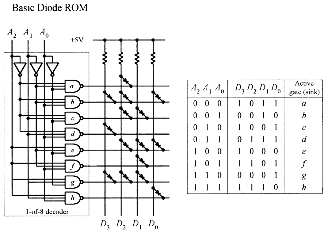
FIGURE 12.144
This is a simple ROM device that uses an address decoder IC to access eight different 4-bit words stored in a diode matrix. Data to be read is output via the D3–D0 lines. The diode matrix is broken up into rows and columns. The intersection of a row and column represents a bit location. When a given row and column are linked together with a diode, the corresponding data output line goes low (0) when the corresponding column is selected by the address decoder via the A2–A0 inputs. When a specific row is addressed, the NAND gate sinks current, so the current from the supply passes through the diode and into the NAND gate's output. This makes the corresponding data line low. When no diode is placed between a given column and row, the corresponding data line goes high (0) when the corresponding row is selected by the address decoder. (There is no path to ground in this case.) In this particular example, we have an 8 × 4 ROM (eight different 4-bit words). By increasing the width of the matrix (adding more columns), it is possible to increase the word size. By increasing the height of the matrix (adding more rows—more addresses), it is possible to store more words. In other words, we could make an m × n ROM.
In reality, today's ROM devices rarely use diode memory cells. Instead, they typically use transistor-like memory cells formed on silicon wafers. Also, a more realistic ROM device comes with three-state output buffers that can be enabled or disabled (placed in a high Z state) by applying a control signal. The three-state buffers make it possible to effectively disconnect the memory from a data bus to which it is attached. (In our simple diode memory circuit, the data is always present on the output lines.) The basic layout, with address decoder and memory cells, is pretty much the same for all memory devices. There are additional features, however, and we'll discuss these in a minute. First, let's cover some memory nomenclature.
12.11.3 Memory Size and Organization
A ROM that is organized in an n × m matrix can store n different m-bit words; in other words, it can store n × m bits of information. To access n different words requires log2n address lines. For example, our simple ROM in Fig. 12.144 requires log2 8 = 3 address inputs (this may look more familiar: 23 = 8). Note that within multiplexed memories and memories that come with serial inputs, the actual physical number of address inputs is ether reduced or the address information is entered serially, along with data and other protocol information.
In terms of real memory ICs, the number of address inputs is typically eight or higher (for parallel input devices at any rate). Common memory sizes are indicated in Table 12.2. Note that in the table, 1K is used to represent 1024 bits, not 1000 bits, as the k (kilo) would lead you to believe. By digital convention, we say that 21 = 2, 22 = 4, 23 = 8, … 28 = 256, 29 = 512, 210 = 1,024 (or 1 K), 211 = 2,048 (or 2 K), … 218 = 262,144 (256K), 219 = 524,288 (540 K), 220 = 1,048,576 (or 1 M, for mega), 221 = 2,097,152 (2 M), … 230 = 1,073,741,824 (or 1 G, for giga), and so on.
TABLE 12.2 Common Memory Sizes
NO. OF ADDRESS LINES |
NO. OF MEMORY LOCATIONS |
NO. OF ADDRESS LINES |
NO. OF MEMORY LOCATIONS |
NO. OF ADDRESS LINES |
NO. OF MEMORY LOCATIONS |
8 |
256 |
14 |
16,384 (16 K) |
20 |
1,048,576 (1 M) |
9 |
512 |
15 |
32,768 (32 K) |
21 |
2,097,152 (2 M) |
10 |
1,024 (1 K) |
16 |
65,536 (64 K) |
22 |
4,194,304 (4 M) |
11 |
2,048 (2 K) |
17 |
131,072 (128 K) |
23 |
8,388,608 (8 M) |
12 |
4,096 (4 K) |
18 |
262,144 (256 K) |
24 |
16,777,216 (16 M) |
13 |
8,192 (8 K) |
19 |
524,288 (540 K) |
25 |
33,554,432 (32 M) |
If this convention confuses you, it should. It is not exactly obvious, and leaves you scratching your head. Also, when a data sheet says 64 K, you need to read further to figure out what the actual organization is, say, 2048 × 32 (2 K × 32), 4096 × 16 (4 K × 16), 8192 × 8 (8 K × 8), 16,384 × 4 (16 K × 4), or another system.
In Table 12.2, watch out for terms such as kB, MB, and GB. These terms refer to bytes not bits; the B signifies 1 byte, or 8 bits. This means that a memory that stores 1 kB actually stores 1 K × 8 (8 K) bits of data. Likewise, memories that store 1 MB and 1 GB actually store 1 M × 8 (8 M) and 1 G × 8 (8 G) bits of data, respectively.
12.11.4 Simple Programmable ROM
Figure 12.145 shows a more accurate representation of ROM-type memory. Unlike the diode ROM, each memory cell contains a transistor and fusible link. Initially, the ROM has all programmable links in place. With every programmable link in place, every transistor is biased on, causing high voltage levels (logic 1s) to be stored throughout the array. When a programmable link is broken, the corresponding memory cell's transistor turns off, and the cell stores a low voltage level (logic 0). Note that this ROM contains three-state output buffers that keep the output floating until a low is applied to the Chip Enable 
![]() input. This feature allows the ROM to be interfaced with a data bus.
input. This feature allows the ROM to be interfaced with a data bus.
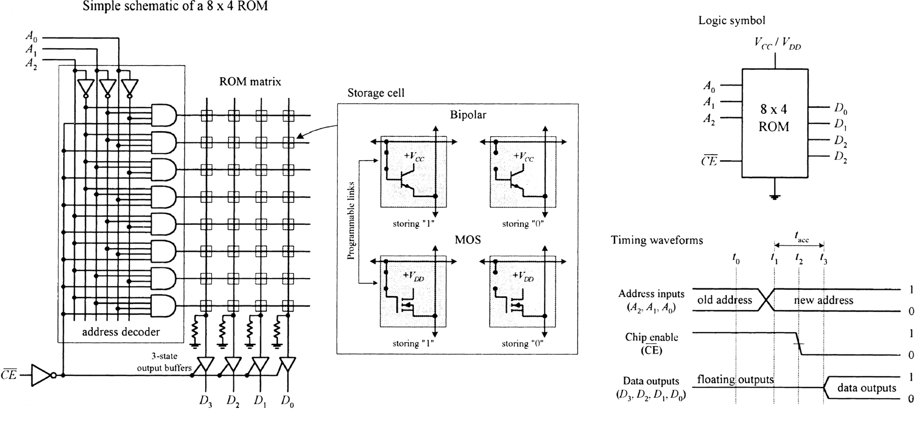
FIGURE 12.145
A basic ROM circuit schematic is shown in Fig. 12.145, along with the appropriate address and chip-enable waveforms needed to enact a read operation. To read data stored at a given address location, the Chip Enable input is set high to disable the chip (remove old data from data outputs)—see time t0. At time t1, a new address is placed on the 3-bit address bus (A2, A1, and A0). At time t2, the Chip Enable input is set low, which allows addressed data stored in memory to be output via D3, D2, D1, and D0.
In reality, the stored data is not output immediately but is delayed for a very short time (from t2 to t3) due to the propagation delay that exists between the initial chip enable signal and the signal that reaches the enable leads of the output buffers. In memory lingo, the time from t1 to t4 is referred to as the access time, which is between around 10 ns and a couple hundred nanoseconds, depending on the specific technology used.
Now two important questions need addressing:
- How does one "break" a programmable link? In other words, how do we program the ROM?
- Is it possible to restore a broken programmable link back to its unbroken" state? In other words, is it possible to reprogram the ROM?
These lead to the next topic.
12.11.5 ROM Devices
There are basically two kinds of ROMs: those that can be programmed only once and those that can be reprogrammed any number of times. One-time programmable memories include the mask ROM (MROM) and the programmable ROM (PROM). ROMs that can be reprogrammed include the erasable programmable ROM (EPROM), electrically erasable programmable ROM (EEPROM), and flash memory.
MROM
An MROM is a custom memory device that is permanently programmed by the manufacturer simply by adding or leaving out diodes or transistors within a memory matrix. In order to create a desired memory configuration, you must supply the manufacturer with a truth table stating which data configuration is desired. Using the truth table, the manufacturer then generates a mask that is used to create the interconnections within the memory matrix during the fabrication process.
As you can imagine, producing a custom MROM is not exactly cheap; in fact, it is rather costly (more than $1,000). It is only worthwhile using an MROM if you plan to mass produce some device that requires the same data instructions (for example, program instructions) over and over again—no upgrades to memory needed in the future. In this case, the cost for each IC—after the initial mask is made—is relatively cheap, assuming you need more than a couple thousand chips.
MROMs are commonly found in computers, where they are used to store system operating instructions and data that is used to decode keyboard instructions.
PROM
PROMs are fusible-link programmable ROMs. Unlike the MROM, with PROM devices, data is not etched in stone. Instead, the manufacturers provide you with a memory IC whose matrix is clean (full of 1s). The number of bits and the configuration (n × m) of the matrix vary depending on specific ROM. To program the memory, each fusible link must be blown with a high-voltage pulse (such as 21 V).
The actual process of blowing individual fuses requires a PROM programming unit. This PROM programmer typically includes a hardware unit (where the actual PROM IC is attached), along with programming cable that is linked to a computer (such as via a serial or parallel port). Using software provided by the manufacturer, you enter the desired memory configuration in the program running on the computer and then press a key, which causes the software program to instruct the external programming unit to blow the appropriate links within the IC.
PROMs are relatively easy to program once you have figured out how to use the software, but as with MROMs, once the device is programmed; the memory cannot be altered. In other words, if you mess things up, you must begin afresh with a new chip. These devices were popular some years ago, but today they are considered obsolete.
The most popular ROM-type devices used today are EPROM, EEPROM, and flash memory. These devices, unlike MROM and PROM devices, can be erased and reprogrammed—a very useful feature when prototyping or designing a gadget that requires future memory alterations.
EPROM
An EPROM is a device whose memory matrix consists of a number of specialized MOSFET transistors. Unlike a conventional MOSFET transistor, the EPROM transistor has an additional floating gate that is buried beneath the control gate—insulated from both the control gate and drain-to-source channel by an oxide layer (see Fig. 12.146).
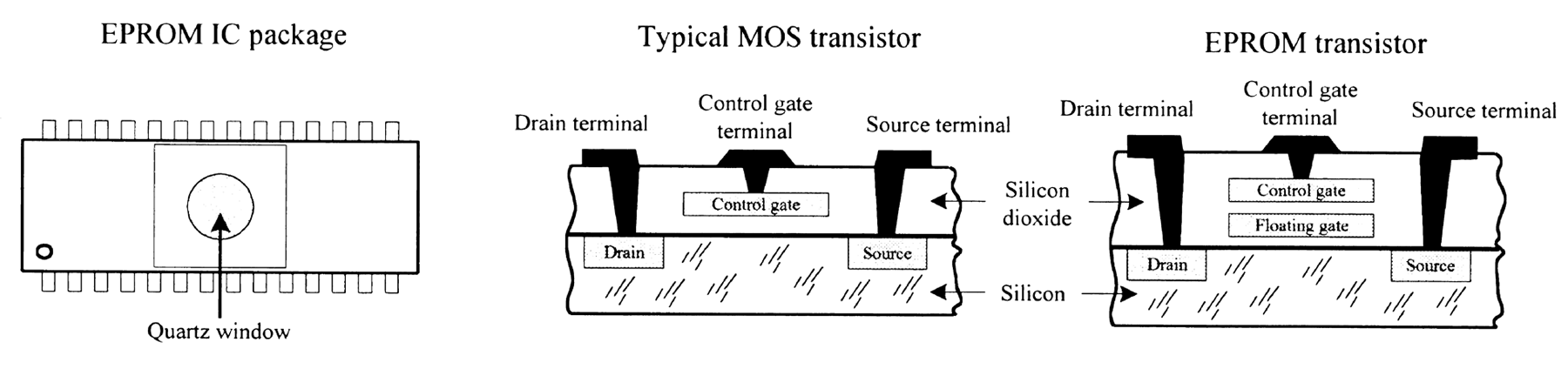
FIGURE 12.146
In its erased (unprogrammed) state, the floating gate is uncharged and does not affect the normal operation of the control gate (which when addressed results in a high voltage or logic 1 being passed through to the data lines). To program an individual transistor, a high-voltage pulse (around 12 V) is applied between the control gate and the drain terminal. This pulse, in turn, forces energetic electrons through the insulating layer and onto the floating gate (referred to as hot electron injection). After the high voltage is removed, a negative charge remains on the floating gate and will stay there for decades under normal operating conditions.
With the negative charge in place, the normal operation of the control gate is inhibited; when the control gate is addressed, the charge on the floating gate prevents a high voltage from reaching the data line—the addressed data appears as a low, or logic 0.
In order to reprogram (erase) an EPROM, you must first remove the device from the circuit and then remove a sticker covering its quartz window. After that, you remove all stored charges on the floating gates by shining ultraviolet (UV) light through the window onto the interior transistor matrix. The UV light liberates the stored electrons within the floating gate region by supplying them with enough energy to force them through the insulation. It usually takes 20 minutes of UV exposure for the whole memory matrix to be erased. The number of times an EPROM can be reprogrammed is typically limited to a couple hundred cycles. After that, the chip degrades considerably.
EPROM is often used as nonvolatile memory within microprocessor-based devices that require the provision for future reprogramming. They are frequently used in prototyping and then substituted with MROMs during the mass-production phase. EPROMs are also integrated within microcontroller chips where their sole purpose is to store the microcontroller's main program (more on this in Chap. 13).
EEPROM
An EEPROM device uses a technology somewhat related to the EPROM, but it does not require out-of-circuit programming or UV erasing. Instead, an EEPROM device is capable of selective memory cell erasure by means of controlled electrical pulses.
In terms of architecture, an EEPROM memory cell consists of two transistors: one transistor resembles the EPROM transistor and is used to store data, and the other transistor is used to clear charge from the first transistor's floating gate. By supplying the appropriate voltage level to the second transistor, it is possible to selectively erase individual memory cells instead of having to erase the entire memory matrix, as is the case with EPROM. The only major disadvantage with EEPROM over EPROM is size—due to the two transistors. However, today, with the introduction of new fabrication processes, size is becoming less of an issue.
In terms of applications, EEPROM is ideal for remembering configuration and calibration settings of a device when the power is turned off. For example, EEPROM is found within TV tuners, where it is used to remember the channel, volume setting of the audio amplifier, and so on when the TV is turned off. EEPROM is also found on microcontrollers, where it can be used to store the main program or to hold other nonvolatile data
Flash Memory
Flash memory is generally regarded as the next evolutionary step in ROM technology that combines the best features of EPROM and EEPROM. These devices have the advantage of both in-circuit programming (like EEPROM) and high storage density (like EPROM).
Some variants of flash memory are electrically erasable, like EEPROM, but must be erased and reprogrammed on a device-wide basis, similar to EPROM. Other devices are based on a dual transistor cell and can be erased and reprogrammed on a word-by-word basis. Flash devices are noted for their fast write and erase times, which exceed those of EEPROM devices.
Flash memories are becoming very popular as mass-storage devices. They are found in digital cameras, where a high-capacity flash memory card is inserted directly into a digital camera and can store hundreds or thousands of high-resolution images. They are also used in digital music players, cellular phones, tablets, and so on.
Microcontrollers often include flash memory to contain their program.
Serial Access Memory
So far, we have seen only memories that incorporated parallel access. These devices sit directly on the address and data buses, making it easy for processors to quickly access the memory. Serial access memory is easy to use in principle; however, since all their address lines are typically tied to an address bus within a microprocessor-based system, it is not uncommon for the data to be inadvertently destroyed when the processor runs amuck (issues an undesired write).
Another type of memory that can "hide" the memory from the processor, as well as reduce the total number of pins, uses a serial access format. To move data to and from memory and the processor, a serial link is used. This serial link imposes a strict protocol on data transfers that practically eliminates the possibility that the processor can destroy data accidentally.
Figure 12.147 shows a few serial EPROM and EEPROM devices from Microchip. The SDA pin found in the EEPROM devices acts as a bidirection data lead used to transfer address and data information into the memory IC, as well as transfer data out to the processor. The SCL pin is the serial clock input used to synchronize the data transfer from and to the device. The 24xx64 and 24LC01B/02B EEPROMs also come with special device address inputs A0, A1, and A2, which are used for multiple device operation. WP is used to enable normal memory operation (read/write entire memory) or inhibit write operations.
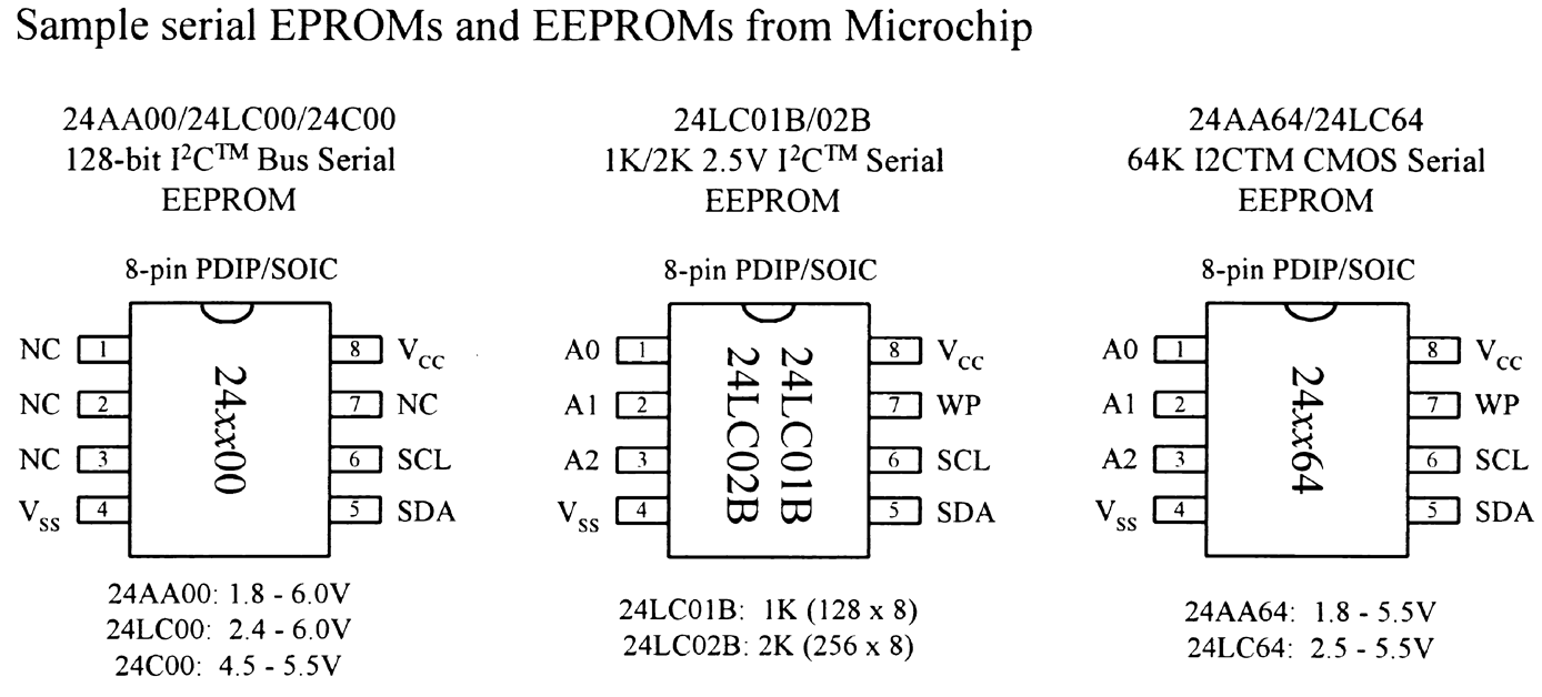
FIGURE 12.147
Controlling a serial memory device is a bit complex, due to the serial protocol and variations in protocol from IC to IC. If you want to learn more about these serial memories (and you should—they are very handy in microcontroller applications for logging data and storing programs and similar tasks), check out the various manufacturers' websites and read through their data sheets.
12.11.6 RAM
The erasable programmable ROM devices, like EEPROM, have limited read/write endurance—around 100,000 cycles—and take considerable time to write to memory. For applications that require constant and quick read and write cycles, it is necessary to use RAM. This type of memory is used for temporary storage of data and program instructions in microprocessor-based applications. Unlike ROM devices, however, RAM devices are volatile, which means they lose their data if power to the IC is interrupted.
There are two basic types of RAM:
- Static RAM (SRAM): In an SRAM device, data is stored in memory cells that consist of flip-flops. A bit that is written into an SRAM memory cell stays there until overwritten or until the power is turned off.
- Dynamic RAM (DRAM): In a DRAM device, a bit written to the memory cell will disappear within milliseconds if not refreshed, or supplied with periodic clocking to replenish capacitor charge lost to leakage.
In general, the major practical differences between SRAM and DRAM include overall size, power consumption, speed, and ease of use. In terms of size, DRAM devices can hold more data per unit area than SRAM devices, since a DRAM's capacitor takes up less space than an SRAM's flip-flop. In terms of power consumption, SRAMs are more energy-efficient because they do not require constant refreshing. In terms of speed and ease of use, SRAMs are superior because they do not require refresh circuitry.
In terms of applications, SRAMs are used when relatively small amounts of read/write memory are needed and are typically found within application-specific ICs that require extremely low standby power. For example, they are frequently used within portable equipment such as pocket calculators. SRAM is also integrated into all modern microprocessors, where it acts as on-chip cache memory that provides a high-speed link between the processor and memory. On the other hand, DRAM is used in applications where a large amount of read/write memory (within the megabyte range) is needed, such as within computer memory modules.
In most situations, you do not need to worry about dealing with discrete RAM memory ICs. Most of the time, RAM is already built into a microcontroller or conventionally housed on PCB memory modules that simply plug into a computer's memory banks. In both these cases, you really do not need to know how to use the memory, because you can let the existing hardware and software take care of the addressing, refreshing, and so on. For this reason, we will not discuss the finer details of the various discrete SRAM and DRAM ICs out there. Instead, we will take a look at some SRAM and DRAM block diagrams that illustrate the basics, and then we will discuss some memory packages, such as SIMMs and DIMMs, that are used within computers.
Very Simple SRAM
Figure 12.148 shows a very elementary SRAM that is set up with a 4096 (4 K) × 1-bit matrix. It uses 12 address lines to address 4096 different memory locations; each location contains a flip-flop. The memory matrix is set up as a 64 × 64 array, with A0 to A5 identifying the row and A6 to A11 identifying the column to pinpoint the specific location to be used. The box labeled "Row Select" is a 6-to-64 decoder for identifying the appropriate 1-of-64 row. The box labeled "Column Select" is also a 6-to-64 decoder for identifying the appropriate 1-of-64 column.
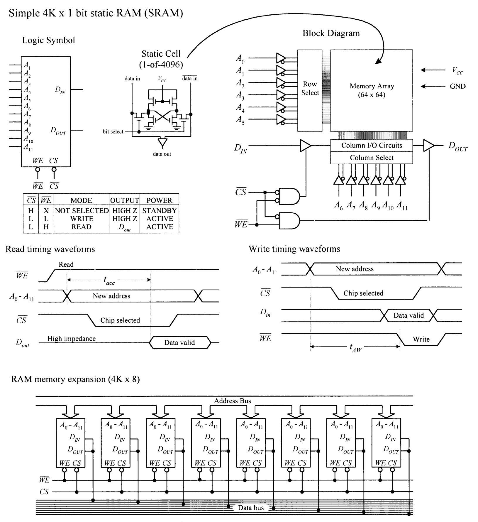
FIGURE 12.148
To write a new bit of data to memory, the bit is applied to DIN, the address lines are set, the Chip Select input ( 
![]() ) is set low (to enable the chip), and the Write Enable input (
) is set low (to enable the chip), and the Write Enable input ( 
![]() ) is set low (to enable the DIN buffer). To read a bit of data from memory, the address lines are set,
) is set low (to enable the DIN buffer). To read a bit of data from memory, the address lines are set, ![]() is set low, and
is set low, and ![]() is set high (to enable the DOUT buffer). See the timing waveforms in Fig. 12.148.
is set high (to enable the DOUT buffer). See the timing waveforms in Fig. 12.148.
By combining eight 4 K × 1 SRAM ICs together, as shown in the lower circuit in Fig. 12.148, the memory can be expanded to form a 4 K × 8 configuration, which is useful in simple 8-bit microprocessor systems. When an address is applied to the address bus, the same address locations within each memory IC are accessed at the same time. Therefore, each data bit of an 8-bit word applied to the data bus is stored in the same corresponding address locations within the memory ICs.
There are other SRAM ICs that come with configurations larger than n × 1. For example, they may come in, say, an n × 4 or n × 8 configuration. As with the n × 1 devices, these SRAMs can be expanded (two n × 8 devices could be combined to form an n × 16 expanded memory, four n × 8 devices could be combined to form an n × 32 expanded memory, and so on).
Serial SRAM with a similar interface to serial EEPROM is also available. For an example of the types of serial SRAM available see http://ww1.
Note on Nonvolatile SRAMs
In many applications, it would be ideal to have a memory device that combines both the speed and cycle endurance of an SRAM with the nonvolatile characteristics of ROM devices. To solve this problem, manufacturers have created what are called nonvolatile SRAMs. One such device incorporates a low-power CMOS SRAM together with a lithium battery and power-sensory circuitry. When the power is removed from the chip, the battery kicks in, providing the flip-flops with sufficient voltage to keep them set (or reset). SRAMs with battery backup, however, have limited lifetimes due to the life expectancies of the lithium batteries—around ten years.
Another nonvolatile SRAM that requires no battery backup is referred to as nonvolatile RAM (NOVRAM). These chips incorporate a backup EEPROM memory array in parallel with an ordinary SRAM array. During normal operation, the SRAM array is written to and read from just like an ordinary SRAM. When the power supply voltage drops, an onboard circuit automatically senses the drop and performs a store operation that causes all data within the volatile SRAM array to be copied to the nonvolatile EEPROM array. When power to the chip is turned on, the NOVRAM automatically performs a recall operation that copies all the data from the EEPROM array back into the SRAM array. A NOVRAM has essentially unlimited read/write endurance, like a conventional SRAM, but has a limited number of store-to-EEPROM cycles—around 10,000.
DRAM
Figure 12.149 shows a very basic 16 K × 1 DRAM. Normally, to access all 16,384 memory locations (capacitors) would require 14 address lines. However, in this DRAM (as within most large-scale DRAMs), the number of address lines is cut in half by multiplexing.
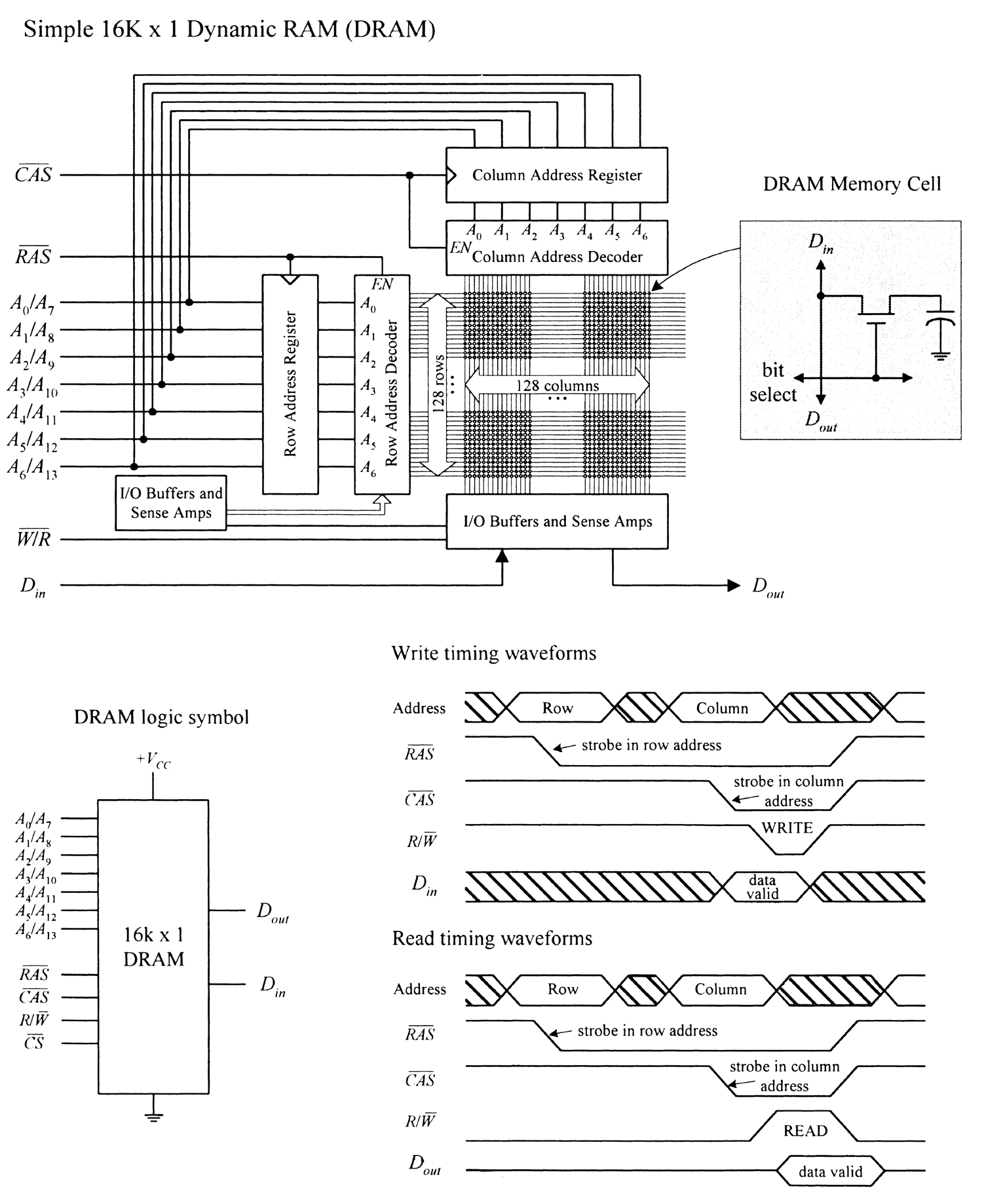
FIGURE 12.149
To address a given memory location is a two-step process. First, a 7-bit row address is applied to A0–A6, and then Row Address Strobe 
![]() is sent low. Second, a 7-bit column address is applied to A0–A6, and then Column Address Strobe
is sent low. Second, a 7-bit column address is applied to A0–A6, and then Column Address Strobe 
![]() is sent low. At this point the memory location is latched and can now be read or written to by using the
is sent low. At this point the memory location is latched and can now be read or written to by using the ![]() input. When
input. When ![]() is low, data is written to the RAM via Din. When
is low, data is written to the RAM via Din. When ![]() is high, data is read from the RAM via Dout. See the timing waveforms in Fig. 12.149.
is high, data is read from the RAM via Dout. See the timing waveforms in Fig. 12.149.
Simple DRAM devices like this must be refreshed every 2 ms or sooner to replenish the charge on the internal capacitors. For our simple device, there are three ways to refresh the cells: use a Read cycle, use a Write cycle, or use an 
![]() -only cycle. Unless you are reading or writing to and from all 128 rows every 2 ms, the
-only cycle. Unless you are reading or writing to and from all 128 rows every 2 ms, the ![]() -only cycle is the preferred technique. To perform this cycle,
-only cycle is the preferred technique. To perform this cycle, 
![]() is set high, A0–A6 are set up with the row address 000 0000,
is set high, A0–A6 are set up with the row address 000 0000, ![]() is pulsed low, the row address is then incremented by 1, and the last two steps are repeated until all 128 rows have been accessed.
is pulsed low, the row address is then incremented by 1, and the last two steps are repeated until all 128 rows have been accessed.
As you can see, needing to come up with the timing waveforms to refresh the memory is a real pain. For this reason, manufacturers produce DRAM controllers or actually incorporate automatic refreshing circuitry within the DRAM IC. In other words, today's DRAMs have all the "housekeeping" functions built in. Practically speaking, this makes the DRAM appear static to the user.
DRAM technology is changing very rapidly. Today, there are a number of DRAM-like devices that go by such names as ECC DRAM, EDO DRAM, SDRAM, SDRAM II, RDRAM, and SLDRAM (we will discuss some of these at the end of this chapter).
Computer Memory
As mentioned, you typically do not need to worry about RAM. (The only real exception would be NOVRAM that is used in many EEPROM-like applications.) RAM is usually either already integrated into a chip, such as a microcontroller, or is placed in reduced pin devices like single in-line memory modules (SIMMs) or dual in-line memory modules (DIMMs) that slide (snap) into a computer's memory bank sockets. In both cases, not much thought is needed—assuming you are not trying to design a microcontroller or computer from scratch. The main concern nowadays is figuring out what kind of RAM module to buy for your computer.
Within computers, RAM is used to hold temporary instructions and data needed to complete tasks. This enables the computer's CPU to access instructions and stored data in memory very quickly. For example, when the CPU loads an application, such as a word processor or page layout program, into memory, the CPU can quickly find what it needs, instead of needing to search for bits and pieces from, say, the hard drive or external drive. For RAM to be quick, it must be in direct communication with the computer's CPU. Early on, memory was soldered directly onto the computer's system board (motherboard). However, over time, as memory requirements increased, having fixed memory onboard became impractical. Today, computers house expansion slots arranged in memory banks. The number of memory banks and the specific configuration vary, depending of the computer's CPU and how the CPU receives information.
Historically, computers initially used either SIMM or DIMM memory modules. Both types of modules use dynamic RAM ICs as the core element. The actual SIMM or DIMM module resembles a PCB and houses a number of RAM ICs that are expanded onboard to provide the necessary bit width required by the CPU using the module. To install a SIMM or DIMM module, simply insert the module into one of the computer memory banks sockets found on the motherboard. Many computer systems use 168-pin DIMMs. Older Pentium and later 486 PCs commonly use 72-pin SIMMs, while still older 486 PCs commonly use 30-pin SIMMs.
A variation on standard sizes of DIMM memory is the SODIMM. SODIMM (Small Outline DIMM) are electrically the same as standard DIMMs but smaller in size and intended for use in laptop computers.
DIMMs
DIMMs have opposing pins electrically isolated to form two separate contacts. DIMMs are often used in computer configurations that support a 64-bit or wider memory bus.
Each new generation of memory brings with it new formats of DIMM, with strategically placed slots to prevent accidental insertion of the wrong type of memory.
DDR3 memory comes in 240-pin DIMMs. Figure 12.150 shows a somewhat simpler sample package from an old 16 M × 64-bit synchronous DRAM that comes in a 168-pin DIMM package.
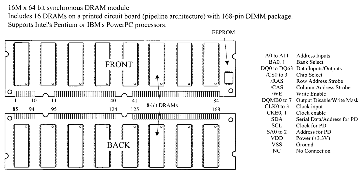
FIGURE 12.150
DRAM Technology Used in Computer Memories
A number of DRAM technologies are incorporated into computer memory modules these days. Extended data out (EDO) memory is a technology that allows the CPU (ones that support EDO) to access memory 10 to 20 percent faster than standard DRAM chips.
Another variation of DRAM is the synchronous DRAM (SDRAM), which uses a clock to synchronize signals input and output on a memory chip. The clock is coordinated with the CPU clock so the timing of the memory chips and the timing of the CPU are in synch. Synchronous DRAMs save time in executing commands and transmitting data, thereby increasing the overall performance of the computer. SDRAM allows the CPU to access memory approximately 25 percent faster than EDO memory.
Double-data-rate SRAM (DDR or SDRAMM II) is a faster version of SDRAM that is able to read data on both the rising and falling edges of the system clock, thus doubling the data rate of the memory chip. Rambus DRAM (RDRAM) is an extremely fast DRAM technology that uses a high-bandwidth "channel" to transmit data at speeds about ten times faster than a standard DRAM.