
Chapter 3: Identifying the Components of Your Target
In this chapter, you will learn, based on an easy-to-get embedded system, how to identify components, make educated guesses about which functional block they belong to, and how to set up a piece of documentation that will help us understand the relationships between the components during our test.
The following topics will be covered in this chapter:
- Harvesting information – reading the fine manual
- Harvesting information – researching on the internet
- Starting the system diagram
- Continuing system exploration – identifying and putting components in the diagram
Let's get started!
Technical requirements
The following are the hardware requirements for this chapter:
- A test system so that you can apply the techniques and tools we will go through in this chapter. I will be using a simple children toy (a Furby, in this case; you can find one pretty easily on private sales websites or second-hand stores) as an example. You may wish to use one or more test systems (I strongly advise that you have more than a single test system available when doing hardware pentesting as it is very common to destroy components or modules during your research; a lot of things can go wrong, and having two to three test systems upfront will save you quite a bit of time) yourself if you want to follow along (some minor details could change depending on the version you get) or use another cheap kid's toy (or any other simple system for that matter) to deploy the same logic on your own.
- Some sharp tools (scalpels or hobby knives).
- Cutting pliers, wire strippers, and electrical tape.
- An entry-level multimeter will be necessary.
- Some screwdrivers may come in handy.
- A clean, white, stable working work surface, in a well-ventilated (but without an air draft) room that you can leave as-is during the course of multiple days of work (best reason ever to send the tenants of open spaces to hell...) is strongly recommended.
- If possible, try to get anti-static mats since the product you will be working with is static-sensitive (assuming that you don't know that already).
- A good quality chair, since you will spend quite a long time sitting down and working.
- Another desk with your main system set up on it and an internet connection is also a must-have.
Please read the safety tips in Chapter 1, Setting Up Your Pentesting Lab and Ensuring Lab Safety, again.
Install your favorite (technical) drawing program. Use one that you are familiar with, as long as it allows you to manipulate text and graphical blocks (I use LibreOffice Draw, but if you feel more at ease with any other productivity suite, Inkscape, or just paper and a pencil, that's fine by me).
Harvesting information – reading the manual
This is a very basic and logical act, isn't it? However, you may have a different approach than the average user reading the manual. Your approach will consider each section of the manual and infer what it tells you about the inner workings of the system.
Taking a system analysis approach
The manual will describe the following:
- If and how the system can interact with the environment
- If and how the user can interact with the system
- How the system will inform the user about its internal status
- If (but usually not how) the system interacts with other system
- How the system is powered
The manual will inform us about the following:
- What sensors are present to sense the environment
- Where some sensors are (and sometimes which type) for user interaction
- What display block components are present
- Whether some networking capabilities are present
Now, let's look at our Furby manual.
For our Furby manual
We will read the Furby's manual and infer some information from it:
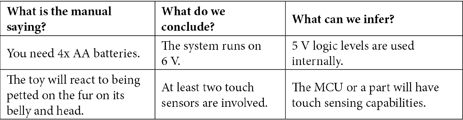

By simply going through the manual, we have been able to gather information about the system without opening it at all.
Harvesting information — researching on the internet
Scour the internet for all the information you can find – anything that could be useful for your project.
The following information sources are of particular interest:
- Manuals for the main system or add-ons.
- Support/repair manuals for the main system or add-ons.
- Patents related to the system.
- Academic articles and known flaws and attacks on the technologies you know the system uses.
- User groups and wikis.
- Previous research that's been done regarding the system (existing vulnerabilities, articles, "Maker" analysis of the product, and more).
- Mobile phone application stores.
- If the system uses radio communication and is sold in the US, there will be a Federal Communication Commission (FCC) filing with an FCC number indicated on the system.
Now, let's look at what we'll need for the Furby.
For the Furby
I have been able to find out the following information regarding the Furby:
- One patent directly linked to the toy, US6544098, which was filed in 1998 by David Mark Hampton and Caleb Chung.
- This patent covers an older version of the toy; some descriptions may not be extremely accurate regarding the current version:


There are multiple user communities dedicated to getting the most out of their toys. From there, I retrieved the following information:

Multiple teardown videos show the following:

There are three different versions for Android phone and a single one for iPhone:
- APKs for Android have been downloaded for further investigation
- The assembly source code for an older version of the toy has been leaked (this is very interesting, but since it is not entirely legal, I will not link it here):
- Downloaded for further investigation
Starting the system diagram
The system diagram will be one of the main documents we will use to identify the various components and subsystems. I will be using LibreOffice Draw to do this (it's free and you can use it too if you so wish), but you can use whatever diagram software you like or even a whiteboard or pen and paper – it doesn't really matter.
In this schema, I have the seven blocks that were presented in Chapter 1, Setting Up Your Pentesting Lab and Ensuring Lab Safety (Power, Networking, Storage, CPU, Sensor, Actuator, and Interface).
You will be able to find a template and multiple versions in the repository for this book.
Before you get started, establish a convention for yourself. My personal convention is as follows:
- Empty rectangles for blocks.
- Ovals for components, with the background color indicating the level of confidence I have in the information.
- Arrows for buses or data paths.
- Lines for power control or analog connections.
I also color code the objects according to the confidence level I have in them:
- Green: It's certain at this point.
- Yellow: I am reasonably certain that it exists, but I have doubts about the details (such as the exact model).
- Orange: It should be there, but I have reasons to doubt its presence.
- Red: Changed my mind but not ready to delete it yet.
For our Furby
You will be able to find the functional schema for this stage in the GitHub repository for this book, which can be found at ch3/functional_diagram_1.odg.
In the following diagram, we can see how the components have been ventilated between the different functional blocks:

Figure 3.1 – Components in blocks
Now, let's explore the system in more detail.
Continuing system exploration – identifying and putting components in the diagram
We will power on the system as described in the manual; that is, we'll insert the required number of batteries and boot the system.
Start interacting with it, learn where the sensors are, try to feel around to see where certain things are, look for where the screws are, and get a general feeling for the system.
Opening the Furby
From now on, it is recommended that you do the following:
- Be smart and take precautions – you will be dealing with pointy, sharp, and other objects that can hurt you. At the end of the day, you will only be losing 30 seconds of your life and sparing yourself a trip to E.R.
- Take note of which screw goes where. Put all screws, bits, nuts, bolts, and pieces in a nice bowl, magnetic recipient, or sorting tray if available.
- Document as much as possible and take pictures of everything (the higher the definition, the better). You will forget things 3 or 4 days down the road (yes, this gray cable harness, the left one, was it for connector A or B?). Again, these 30 seconds feeling like a tourist and taking plenty of pictures will save you an afternoon trying to figure out whether the weird gray thing was holding piece X or Y in place.
Manipulating the system
We will also be manipulating the system (in that we will be touching it with our hands, moving it while it's open, screwing it, unscrewing it, probing it, turning it, and more). Embedded systems are not engineered for this at all; they are made to sit firm while being held by screws, glue, and plastic supports. Out interference may actually damage the system, so we should take the following precautions to prevent this and to protect ourselves from accidents:
- Reread the safety directions provided in Chapter 1, Setting Up Your Pentesting Lab and Ensuring Lab Safety.
- Wires soldered to the PCB are not made to move a lot, be pulled, torn, and support all of the abuse that we will inevitably put on them. I like to put a blob of hot glue on the solder joint, which acts as a force relief and prevents the actual copper in the wire from moving (copper tends to break easily).
- Plastic connectors tend to easily rip from the PCBs, especially when they have plastic clasps that hold them securely and you unplug/plug them repeatedly. I like to remove the clasps with a scalpel blade and secure the connector to the PCB with a bit of cyanoacrylate glue.
- Some battery powered systems don't have an on/off switch and removing the batteries can be tiring. Get in there and add an on/off switch just next to the batteries. This will save you a lot of time (unless you're forced to do otherwise, add the switch to the wire connected to the positive side of the batteries and hot glue it securely in place).
- Probing and holding a PCB at the same time is hard, so get yourself a PCB vise or, even better, one of those PCB workstations with articulated arms that can be 3D printed or bought on eBay.
- Some systems don't have an on/off visual indicator. Most of the time, it's just a matter of adding a LED and a resistor.
- If the system is mains powered or connected to an equally dangerous power source (these 12 V/56 A server PSUs can grill meat just fine if you are unlucky enough for the current to start flowing), find a way to add a very visible, very obvious "I AM PLUGGED IN TO DEADLY POWER" indicator – it's not because the system is sleeping that the mains/high energy won't kill you. For this, I use a lamp with a red bulb, placed in parallel to the extension cord, for projects like this, as well as an isolation transformer.
Dismantling the Furby
You will be able to find the dismantling picture in the GitHub repository for this book, in the ch3/dismantling_pictures folder.
Identifying chips
Take pictures (as readable as possible) of every circuit board, in relationship to others and themselves.
Take closeups of every chip and module you find.
Identify the markings (if they have not been rubbed off or erased) and try to identify the package. The package is the name of the physical package the chip comes in. There are plenty of them – some standard, some not. Please refer to https://en.wikipedia.org/wiki/List_of_integrated_circuit_packaging_types as a basic way to identify them. There is no other means to memorize and recognize them but to see and use plenty of different ones.
Chips in the Furby
We will now try to get a general sense of how to find more detailed information about chips. Since we found the chips in the Furby, we need to know what they are doing. We can learn about them by looking at the part numbers on the chips and identifying the package family.
Main package families and markings
You should be able to identify the following packages:


On top of the chips, there are markings, which are usually as follows:
- Some kind of company logo
- A model reference number
- A lot number and/or fabrication date
Normally, the markings are written in white, but they can wear out. In this case, just a little bit of spit rubbed on it (or solvent if you are squeamish) may make them easier to see.
Sometimes, markings are lasered or sanded off. In this case, you can usually identify the chips by studying their function and pinout.
The best way to find out information about a chip is to do a quick internet search:
- On a general search engine: The markings we found and datasheet. This will (hopefully) give us a document that describes the chip's behavior and connections.
- On websites dedicated to electronic components (mouser, DigiKey, element14, arrow, and so on): The markings should link us to a page (if the site sells the component), along with a link to the datasheet.
Here, we can find the following information:


Now, let's learn how to identify unmarked/mysterious chips.
Identifying unmarked/mysterious chips
This is a trickier activity; it is not uncommon for a vendor to erase markings/use an unmarked chip (or even have their own marking put on the chip) in order to impede their products from being analyzed or replicated.
Identifying an unknown chip boils down to performing an investigation:
- The environment:
- What other chips did you identify that are connected to it?
- What are its suspected functions? (Is it connected to a storage chip, an MCU, or an analog sensor? Does it act as glue logic between an MCU and a peripheral?)
- The chip itself:
- What package is the chip using? Is it through-hole or surface mount? How many legs (leads) does it have?
- Can we identify pin functions? (Are some pin(s) connected to the ground? Are they connected to the power rails? Are they used as an analog to digital (ADC) converter or digital to analog (DAC) converter? Are they connected to actuators?)
- Once powered, what voltage is it powered with?
- Is it using an external oscillator (a crystal or another form of oscillator)?
With this information in mind, you can then go to a chip vendor website. These websites (DigiKey, Mouser, Keil, and so on) usually propose a parametric search engine where you can input your data. You will generally end up with a handful of candidates across websites (not every vendor sells chips from all chip makers). Harvest the datasheets for the aforementioned candidates and match your chip's connections with the pin-out of the adequate footprint/package.
Epoxy blobs
Epoxy blobs (they look like black epoxy resin blobs) are very common in high-volume products (that is, systems that are produced in very high numbers for which every tenth of a cent saved counts). They are usually hiding one or more die.
Information Box
A die is the actual piece of silicon for the chip. Typically, when you picture a chip in your mind, you think of a more or less square, black plastic object. This is actually what is called a package; that is, a die enclosed in an epoxy package with its electric contacts (the pads) wired to "legs" (the leads).
Often, packaging a die (that is, putting it in a plastic case, adding the lead, bonding the pads to the lead with gold wire, and so on) can cost a fair amount of money with respect to the cost of the die itself. So, if the product is made in large numbers, if the die is very cheap or if the die is custom-made for the application, it can make economic sense to directly wire the pads to the traces on the printed circuit board (PCB). Epoxy blobs can prove difficult to work with since the tricks used to identify chips (using the pinout of the package and so on) don't really make sense anymore. Looking into the signals that get in and out of the blob can help in identifying these functions. It is possible to remove the epoxy using dangerous chemicals and inspecting the exposed die with a microscope, but this is an advanced technique that requires significant know-how and that goes beyond the scope of an introductory book.
Furby — the mystery meat
In this section, we will look at the components we had trouble identifying. Here, the goal is either to identify them formally or get the best idea possible about their functionality/roles.
Z100401K9 and 3D3G
We were unable to find references for Z100401K9 and 3D3G. These chips are on a daughterboard, where we suspect the main MCU is located. Let's start probing around with our multimeter.
Please read your multimeter's manual and familiarize yourself with operating it (the same applies to all your tools, actually). We will be using two of its most common modes of operation:
- Direct current voltage reading (also known as DC, as in the kind you find across a battery where the voltage stays the same, as opposed to AC, which is the kind you find in the wall plug where the voltage varies periodically between two voltages). This DC voltage reading tells you the voltage (the difference of potential) between your two probes. Since voltage only has a difference between TWO points, the usual point of reference is called ground (also marked as GND for short). The usual ground is (for DC circuits) the negative pole of your batteries, but (and I must really insist this because it confuses a lot of people when they are starting) this is just a way to call a shared reference point. Measuring this only makes sense when the toy is turned on.
- A continuity test, which tells you if there is a direct path (that is, a simple wire) between your two probes. Do this with the tool turned off completely (that is, batteries removed). When you place your probes between two points that are connected, your multimeter will beep.
By probing around the two chips, we can identify the following connections:

Figure 3.2 – Probing the power section chips
The round component marked 470 with a PCB reference of L6 is an inductor (that is, a coil), D6 is a diode, and C58 (to the right of D6) is a capacitor.
They are arranged as follows:

Figure 3.3 – Equivalent schematic for the Z100
This is a very typical step-up transformer. This is used to maintain a high enough voltage for the rest of the circuit to function properly when the battery voltage starts to decrease (batteries have a discharge curve where the voltage goes down with the charge). I strongly encourage you to have a look at the different types of topology available. You don't need to learn them off by heart (unless you are an electrical engineer, in which can you probably know them already) – knowing what they are and how to find their references is much more important.
3D3G is a typical 3.3 V LDO that's used to provide the circuit with the 3.3 V needed by the components. There are a few voltages (called logic levels) that are very typical for chips to be powered with or to communicate over. The most classic is 5 V (called TTL), which is still present today mainly for compatibility reasons. 3.3 V is the most common as of today, but lower voltages are becoming more and more common (1.8 V, 1.2 V, 0.95 V) to limit consumption and heat dissipation while having faster clocks.
Both of these components can be found in the power block.
The green module with an epoxy blob
First, with your multimeter in continuity mode, you can find out which pin is the ground pin. Weirdly, I didn't find a pin connected to neither the batteries (we will call this VBAT), the boosted output of the batteries (we will call this VBATB), or the 3.3 V rail. Maybe this IC is only provided with power when consumption needs to be reduced (this will later prove to be right)? By probing around, we can find out that the two pins are connected to the High Speaker. One is indeed switching to 3.3V shortly before the toy "speaks," and two pins read varying voltage levels (this can be a sign that these can actually be digital buses).
Let's take note of the pinouts:

Figure 3.4 – Pinout of the green module
We can confirm if the pins are digital buses or not by looking at the signal using either a logic analyzer or an oscilloscope (two really useful tools you will really, really want to have in your toolbox).
An oscilloscope is, simply put, a very fast multimeter that regularly reads the voltages between the probe point and a reference point (usually an alligator clip attached to the probe) and shows you the value of these samples as a function of time.
By looking at the signal on a scope, we will no signal structure that actually looks like a digital signal (digital signals usually toggle between a high and a low state in quite clear states and don't linger somewhere in the middle). It is more likely that this module is actually just acting as an (inverting) audio amplifier, as shown in the following image:

Figure 3.5 – Traces of the signals on the oscilloscope
The preceding image was extracted from my oscilloscope through a dedicated vendor utility. When you look at the dynamics of the signal, signal 1 (the middle line) has a very low amplitude (the scale is 200 mV/Div) that matches the behavior of the signal that is going through the speaker (signal 2, the lower line, with a scale of 2 V/Div).
This module goes into the interface block.
The blue module with an epoxy blob
This module is marked FR and all my test toys are French-speaking, which means this may be responsible for speech synthesis. Let's probe around and identify the pins:

Figure 3.6 – The SPI blue module
From our naming convention, we can expect a Serial-Parallel Interface (SPI) style communication. SPI will be covered in Chapter 6, Sniffing and Attacking the Most Common Protocols. Let's probe these pins while they're functioning to verify if there's correlation with the sounds:
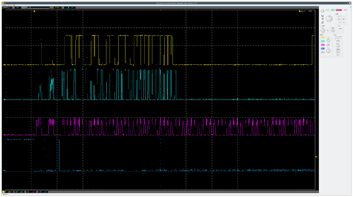
Figure 3.7 – Traces of the SPI signal on the oscilloscope
The following is an zoomed-in image showing the start of the signal:

Figure 3.8 – Zoomed-in version of the start of the signal
Indeed, these signals (one clock, one data in, one data out, and a chip enabled) are very typical of SPI (I will go through the typical protocols used for chip-to-chip communication in Chapter 6, Sniffing and Attacking the Most Common Protocols). The sip_wp (typos on PCB silkscreens are not uncommon; the engineer typed sip instead of spi – wp is a very common shorthand in datasheets for write protection) test pad connected to the pin between the ground and power (3.3v pin) hints at a SPI EEPROM. Maybe the data for speech synthesis is stored here. At this point, we may not want to be too destructive, so we should lift the module and try to dump and reprogram it at a later stage. We can note that down on our functional diagram. This could actually be the SPI EEPROM, as discussed in the patent, and the ATMLH306 may be used for something else (storing the general status of the "learning" of the toy, maybe?).
This module probably goes in the storage block.
A big epoxy blob behind the eyes' LCD
This is a contender for hiding the main MCU (and possibly other dies).
This blob has a very large number of traces exiting from it since it is directly driving an LCD with a fair number of pixels in it. It is possible that there is a dedicated LCD driver die hidden under the epoxy.
By following traces with our multimeter (and with the help of a very fine needle to follow vias from side to side of the PCB (a via is a hole in the fiberglass that is plated with a conductive material to allow a trace to jump from one side to the other or a layer to another, so when you see a trace ending on a hole or with a hole in it, that's a via), we can see (by probing with our multimeter in continuity mode) that it is connected to the following:
- The LCD's zebra strips (a zebra strip, also known as an elastomeric connector, is a flexible piece of foam that has conductive zones).
- A 32,768 Hz crystal (this is commonly used for RTCs, though it is better for time stability for the driver of communication protocols).
- The piezo element we suspect is the emitter for networking (it's in parallel with a 3.3 mH inductor and driven through a transistor, but it could also be driven from the IR output of the TSP50C04).
- The electret microphone that is acting as the receiver for ultrasound networking. The TSP50C04 is not acting as a receiver, so this module isn't hosting only this die (or the die that performs voice synthesis).
- The SPI EEPROM.
- The ATMLH308 i2C EEPROM.
- The movement sensor on the green daughter board.
The variety of protocols, buses, and peripherals it is connected to doesn't leave any room for doubt: this is where the MCU die is hosted. We can also reasonably assume that the speech synthesis die is also hosted under the same epoxy blob. This blob is not a single component and will not appear in the functional diagram as such, but this investigation allowed us to locate two very important components (the MCU and screen driver).
An epoxy blob on the side PCB
This module is actually a "daughterboard" that's connected perpendicularly to the main PCB. There is a soldered bus toward the main blue PCB that has 17 connections toward it. We have already seen that the main power regulation, as well as the motor driving and sensing, happens on this daughterboard. This board also hosts a sensor that is probably acting as a position sensor (a black box that makes spring/rattling noises when tapped, probably an archaic multi-axis vibration/acceleration sensor that the toy uses to sense when it is being shaken).
The blob is connected to the following:
- The aluminum sticky tapes, which are used as touch sensors
- The AT5561S (H bridge/motor driver).
- The SPI bus (marked on the connector).
This is probably a cheap general-purpose MCU acting as a slave for motor driving and touch sensing.
The borders of functional blocks
As we have seen from our example systems, a component can sometimes fulfill functions in multiple blocks (for example, our side MCU). In this case, I like to split the component into two sub-components that I can put in their respective blocks.
Sometimes, this can be a little bit tricky since, for example, some components are powered from their communication interface (look into the Dallas 1-wire interface) or use a sensor for communication (in our example system, the microphone is used as a sensor for loud sound detection and as a communication receiver for receiving ultrasound). In such cases, the selected block will be to a judgment call. Do not let the functional diagram become a problem for you – it is there to assist you, so just add plenty of annotations and continue your investigation.
Summary
In this chapter, we have learned how to harvest data on a system without having to open it. This process included collecting documentations and pieces that will feed our investigation and reflection process.
We then learned how to open a system and the necessary precautions that we must take when doing so in order to protect our test system and ourselves. This primary approach to the system will feed our ongoing analysis and will allow us to understand how the system will actually implement the functionality it provides to the user.
In the next chapter, we will go through a methodology that will help you assess where the important bits of information are in a system, as well as how to assess how they should be protected.
Questions
The following questions have not necessarily been answered in this chapter, so you may need to do some research on your own. The first part of this chapter was about searching for information on an unknown system. Use your head or your keyboard!
- When you are arranging the contractual framework for pentesting with your client, how many test systems should you request?
- Can you formally guarantee your client that all the test systems that they provided will be returned to them in a full functioning and undamaged state?
- When I was inspecting the green amplifier module, I looked into the pins that were varying to check if these were digital buses or not. Look at the signal from the oscilloscope for these pins and at the signal for actual digital buses for the blue FR module. Do you have any idea why an oscillating signal such as a digital bus can be read as a floating-point value by your multimeter?
- Using a chip vendor website, have a look at the 74HC14 and compare the price of the through-hole package and the surface mount package for the same chip maker. The die inside is exactly the same. What does this tell you?
- The 74HC14 is a member of a logic family called the 74 family. Can you find a another very common logic family? If so, what are the main differences between them?
- What is FCC? What type of system should you try to look for in the FCC database?
- The patent hinted at a 6502-based architecture, but it is not clear if this is still the case in the real system. Is 6502 a Harvard or Von Neumann architecture?