CHAPTER 13
The Power Distribution Network (PDN)
The power distribution network (PDN; sometimes also called the power delivery network) consists of all the interconnects from the voltage-regulator module (VRM) to the pads on the chip and the metallization on the die that locally distributes power and return current. This includes the VRM itself, the bulk decoupling capacitors, the vias, the traces, the planes on the circuit board, the additional capacitors added to the board, the solder balls or leads of the packages, the interconnects in the packages mounted to the board, the wire bonds or C4 solder balls, and the interconnects on the chips themselves.
The primary difference between the PDN and signal paths is that there is just one net for each voltage rail in the PDN. It can be a very large net that can physically span the entire board and can have many components attached.
TIP
As we will see, the PDN is like an ecosystem. If one small part of the PDN changes, the performance of the entire system can be affected. This makes generalizations very difficult.
13.1 The Problem
Figure 13-1 shows an example of a motherboard with all the interconnects mentioned in the preceding section.

The first and primary role of the PDN is to keep a constant supply voltage on the pads of the chips and to keep it within a narrow tolerance band, typically on the order of 5%. This voltage has to be stable, within the voltage limits, from DC up to the bandwidth of the switching current, typically above 1 GHz.
TIP
The purpose of the PDN is threefold: Keep the voltage across the chip pads constant, minimize ground bounce, and minimize EMI problems.
In most designs, the same PDN interconnects that are used to transport the power supply are also used to carry the return currents for signal lines. The second role of the PDN interconnects is to provide a low-impedance return path for the signals.
The easiest way of doing this is by making the interconnects wide, so the return currents can spread out as much as they want and by keeping the signal traces physically separated so that the return currents do not overlap. If these conditions are not met, the return current is constricted, and the return currents from different signals overlap. The result is ground bounce, also called simultaneous switching noise (SSN) or just switching noise.
Finally, because the PDN interconnects are usually the largest conducting structures in a board, carry the highest currents, and sometimes carry high-frequency noise, they have the potential of creating the most radiated emissions and causing failure of an EMC certification test. When done correctly, the PDN interconnects can mitigate many potential EMI problems and help prevent EMC certification test failures.
The consequence of not designing the PDN correctly is that there will be excessive noise on the voltage rails of the chips. This can cause a bit failure directly, or it can mean the clock frequency of the chip can’t be met, and timing errors result.
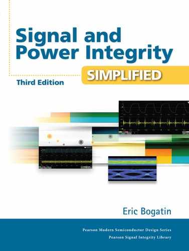
Figure 13-2 shows an example of the voltage noise on the pads of a processor chip. In this example, the nominally constant 2.5-v rail to the core of the chip, referred to as Vdd, shows voltage noise of as much as 125 mV on some pads. As the Vdd supply drops, the propagation delay of the core gates will increase, and timing problems can cause bit failures.

Figure 13-2 Example of the measured voltage between three different pairs of Vdd and Vss pads of a processor chip, showing as much as a 125-mV drop. The initial step down is when the processor comes out of an idle state. The three traces are three different locations on the die. The precise shape is related to the microcode running on the processor.
13.2 The Root Cause
If the problem is a voltage drop or a droop on the power supply rails on the pads of the chip, why not just use a “heftier” regulator—one that can supply a more rock stable voltage? Why not pay extra for a regulator with a 1% regulation or even 0.1% regulation? This way, the voltage from the regulator will be absolutely stable, no matter what, right?
What the chip cares about is the voltage on its pads. If there were no current flow in the PDN interconnects from the regulator pads to the chip pads, there would be no voltage drop in this path, and the constant regulator voltage would appear as a constant rail voltage on the chip pads.
If there were a constant DC current draw by the chip, this DC current would cause a voltage drop in the PDN interconnects due to the series resistance of the interconnects. This is commonly referred to as the IR drop. As the current from the chip fluctuates, the voltage drop in the PDN would fluctuate, and the voltage on the chip pads would fluctuate.
Now add not just the resistive impedance of the PDN but also the reactive components, including the inductive and capacitive qualities of the PDN interconnects. The impedance of the PDN, as seen by the pads on the chip, in general, is some complex impedance verses frequency, Z(f ). This is diagrammed in Figure 13-3.

Figure 13-3 Diagram of the connections from the VRM through the PDN to the chip pads and the voltage drop across the PDN interconnects due to the impedance of the PDN.
As fluctuating currents with some spectrum, I(f ), pass through the complex impedance of the PDN, there will be a voltage drop in the PDN:
where:
V(f ) = voltage amplitude as a function of frequency
I(f ) = current spectrum drawn by the chip
Z(f ) = impedance profile of the PDN, as seen by the chip pads
This voltage drop in the PDN means that the constant voltage of the regulator is not seen by the chip but is changed. In order to keep the voltage drop on the chip pads less than the voltage noise tolerance, usually referred to as the ripple, given the chip current fluctuations, the impedance of the PDN needs to be below some maximum allowable value. This is referred to as the target impedance:

where:
Vripple = voltage noise tolerance for the chip, in volts
VPDN = voltage noise drop across the PDN interconnects, in volts
I(f ) = current spectrum drawn by the chip, in Amps
ZPDN (f ) = impedance profile of the PDN as seen by the chip pads, in Ohms
Ztarget = maximum allowable impedance of the PDN, in Ohms
As mentioned many times so far in this book, the most important step in solving a signal integrity problem is to identify the root cause of the problem. The root cause of rail collapse or voltage noise on the PDN conductors is that a voltage drop in the PDN interconnects is created by the chip’s transient current flowing through the complex impedance of the PDN.
TIP
If we want to keep the voltage stable across the pads of the chip, given the chip’s current fluctuations, we need to keep the impedance of the PDN below a target value. This is the fundamental guiding principle in the design of the PDN.
13.3 The Most Important Design Guidelines for the PDN
The goal of the PDN is to deliver clean, stable, low-noise voltage to the pads of all the active devices that require power. We often translate this performance metric into designing the PDN interconnects to bring their impedance, as viewed from the chips’ pads, below a target value from DC to high frequency. In general, this will be accomplished by following three important design principles. Though it may not always be possible to push these to the limit, it is always important to be aware of the directions to head, even if the real-world constraints keep you from the ultimate path.
The three most important guidelines in designing the PDN are:
1. Use power and ground planes on adjacent layers, with as thin a dielectric as possible, and bring them as close to the surface of the board stack-up as practical.
2. Use a surface trace that is as short and wide as possible between the decoupling capacitor pads and the vias to the buried power and ground plane cavity and place the capacitors where they will have the lowest loop inductance.
3. Use SPICE to help select the optimum number of capacitors and their values to bring the impedance profile below the target impedance.
Unfortunately, in the real world of practical product design, you may not always have the luxury of power and ground planes on adjacent layers or placed near the top of the board stack-up. There may be multiple voltage rails, and they may have odd and irregular shapes, with many antipad clearance holes.
You may not be able to use as many capacitors as you think you need, nor place them in proximity to the devices they are decoupling. Even if you do the best you can, it will still be important to know if it is “good enough” before you build the product. The last place you want to find a problem is when you are making 100,000 units and finding that 1% of them are failing due to excessive noise in the PDN. The time to find this out is as close to the beginning of the design process as possible, and the only way to determine this is by using analysis tools that allow you to explore design space.
TIP
It is essential to try to follow the three important design guidelines above and, at the same time, to use combinations of rules of thumb, approximations, and numerical simulation tools to predict the impedance profiles and voltage noise under typical and worst-case conditions.
The most important principle to follow for cost-effective design is to add appropriate analysis as early in the design cycle as possible. This will reduce the surprises as the design progresses and result in a product with acceptable performance at the lowest cost and that works the first time.
13.4 Establishing the Target Impedance Is Hard
The first step in designing the PDN is to establish the target impedance. This must be done separately and independently for each voltage rail to all the chips on the board. Some designs may use as many as 10 different voltages. In each one, the target impedance may vary with frequency due to the specific current spectrum of the chip.
Suppose that the current from the chip on one rail is a sine wave, with a peak-to-peak value of 1 A. The amplitude of the sine wave of current will be 0.5 A. This current from the chip is shown in Figure 13-4 in both the time domain and the frequency domain.

Figure 13-4 Example of the current waveform in the time domain (top) and the frequency domain (bottom) for a sine-wave current draw.
When this frequency component of the current flows through the specific impedance profile of the PDN, a voltage noise will be generated in the PDN. An example of an impedance profile with the frequency component of the current, and the resulting time-domain voltage noise across the chip pads, is shown in Figure 13-5.

Figure 13-5 Voltage noise on the chip pads (top) as the sine-wave current flows through the PDN impedance profile of simulated PDN (bottom). The spike in the PDN profile at about 20 MHz shows where the sine-wave-frequency component of the current is with respect to the PDN impedance peaks.
When the sine-wave current passes through an impedance that is too large, the voltage generated is above the ripple spec, which is typically ±5%, shown as the reference lines.
There is the potential for the current draw through a chip to be at almost any frequency from DC to above the clock frequency. This means that unless the precise current spectrum from the chip is well known, for all the possible microcode that could be running through it, we have to assume that the peak current could be anywhere from DC to the bandwidth of the signals.
In a few rare cases, if it is known that the chip processing will have a high-frequency fall off the current draw above some frequency, it may be possible to put some constraints on the current spectrum. This should always be done whenever possible.
While the current draw from a chip is rarely a pure sine wave, there are always sine-wave-frequency components in the current. The precise spectrum of the current amplitudes will interact with the impedance profile of the PDN completely independently of each other, but the resulting voltage waves will add together. Sometimes they can add and still meet the ripple spec, while at other times, they can add and exceed the ripple spec, depending on the precise overlap of current peaks and impedance peaks.
Figure 13-6 shows an example of a 1-A peak-to-peak square wave current draw for two slightly different modulation frequencies. The square wave current will have sine-wave-frequency components at odd multiples of the square wave frequency. Above roughly the fifth harmonic, depending on the rise time, the amplitude of the sine-wave harmonics will drop off much faster than 1/f. As the modulation frequency changes, the frequency distribution of the harmonics shifts and interacts differently with the PDN impedance profile.
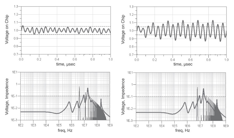
Figure 13-6 The resulting ripple noise when the same 1 A current draw has a slightly different modulation frequency, where one of the harmonic components overlaps an impedance peak of the PDN impedance profile.
A very slight frequency shift in the modulation of the current can mean the difference between acceptable performance and failure. Unfortunately, the engineer designing the PDN has very little control of the current draw spectrum of the chip. It is whatever the chip is going to do, depending on its operation.
This means that unless there is precise information about the specific, worst-case spectrum of the current draw of the chip, a conservative design must assume a worst-case current that could occur at any frequency from DC to the bandwidth of the clock, which is a few times the clock frequency.
In practice, it is not the peak current but the maximum transient current that interacts with the higher frequencies of the PDN. If there is a steady-state DC current draw from the chip, the sense lines of the VRM can usually compensate to keep the rail voltage close to the specified voltage value. It’s when the current changes from the DC value, either increasing or decreasing, at frequencies above the response frequency of the VRM, that the current will interact with the PDN impedance.
The maximum impedance for the PDN, the target impedance, is established based on the highest impedance that will create a voltage drop still below the acceptable ripple spec. This is given by:
or:
where:
Vdd = supply voltage for a specific rail
Itransient = worst-case transient current
ZPDN = impedance of the PDN at some frequency
Ztarget = target impedance, the maximum allowable impedance of the PDN
Vnoise = worst-case noise on the PDN
ripple% = ripple allowed, assumed to be ±5% in this example
The optimum PDN impedance should be below the target impedance but not too far below the target impedance.
If the PDN impedance is kept below the target impedance at every frequency, the worst-case voltage noise generated across it as the worst case, maximum transient current flows through it will be less than the ripple spec. If the PDN impedance is much below the target impedance, it means the PDN was overdesigned and costs more than it needs to.
TIP
Whenever possible, the peak transient current should be used in estimating the target impedance. When the peak transient current is not available, it can be roughly estimated from the maximum current draw or from the power consumption of the chip.
While the worst-case transient current is what is important, rarely is this provided in a spec sheet. Rather, it is the worst-case peak current per rail that is on spec sheets. After all, this is important to estimate how large a voltage regulator module is needed. It must be capable of supplying the maximum current draw at the rated voltage.
The peak current could be mostly DC with a 10% transient current, or it could be a very low quiescent current with most of the peak current being transient that would last only for a few microseconds. Without special knowledge of the behavior of the chips in each application, the conservative design has to plan for the worst case.
What fraction of the maximum current is transient? Obviously, it depends on the function of the chip. It could vary from 1% to 99%, depending on the application. As a rough, general rule of thumb, without any special knowledge, the transient current can be estimated as being half of the maximum current:
where:
Itransient = worst-case transient current from the chip
Imax = maximum total current from the chip
Alternatively, the worst-case power dissipation of the chip will always be provided in a chip’s specs since this is critical information when designing the thermal management approach for the package. It is not usually separated by voltage rail, so some assumptions would have to be made on the power consumption of each rail.
However, given the power consumption per voltage rail, the peak current draw of a chip can be estimated from:
And from this, the target impedance can be evaluated as:
where:
Ipeak = worst-case peak current, in Amps
Pmax = worst-case power dissipation, in watts
Vdd = voltage rail, in volts
ripple% = ripple spec, in %
2 = comes from the transient current being ½ the peak current
For example, if the ripple spec is 5%, the target impedance is:

In the case of a 1-volt rail and 1-watt power dissipation device, the target impedance would be about 0.1 Ohm:
Some chip vendors, especially FPGA vendors, also provide calculation tools that allow simple estimates of the current draw of specific voltage rails, depending on the gate utilization. These can be used to estimate the target impedance specs of the rails. An example of the results of using one such analysis for the Altera Stratix II GX FPGA is shown in Figure 13-7.

Figure 13-7 Example of a calculation of the target impedance of different voltage rails based on gate utilization of an Altera FPGA.
Finally, the current requirements of the I/O voltage rails, typically referred to as either the Vcc or Vddq rails, can be estimated based on the number of gates that are switching.
If each output gate drives a transmission line with some characteristic impedance, then the load it sees, if only for a round-trip time, is the same as the characteristic impedance of the line it drives.
If n gates could switch simultaneously, the transient current draw could be:
And the target impedance of the VCC rail would be:
Itransient = worst-case transient current
n = number of I/Os that could switch simultaneously
Vcc = voltage rail
Z0 = characteristic impedance of the transmission lines
For example, if the lines are all 50 Ohms, and there are 32 bits switching simultaneously, the target impedance for the Vcc rail would be:
Even with the peak current and the target impedance established, the current could be fluctuating at almost any frequency due to the specific microcode or application running. This means that unless there is information to the contrary, it must be assumed this is the target impedance, flat from DC to very high frequency.
TIP
The goal in designing the PDN is to keep the impedance of the PDN interconnects below this target value over a very wide bandwidth. A PDN above the target impedance may result in excessive ripple. A PDN impedance much below the target impedance may be overdesigned and more expensive than it needs to be.
When the impedance profile is kept below the target value, the worst-case voltage rail noise will be less than the ripple spec. An example of a successful impedance profile is shown in Figure 13-8.

Figure 13-8 When the impedance profile (bottom) is below the target impedance, the worst-case voltage noise (top) is below the ripple spec. The square wave is the current draw by the chip, while the flat curve is the voltage on the supply rail.
However, if there is a peak in the impedance profile that exceeds the target spec, and if the worst-case current happens to fall on top of this peak impedance, there is a chance that the ripple spec may be exceeded. This is shown in Figure 13-9. In this example, the step current change excites the peak impedance, and we see the characteristic ringing at the peak frequency.

Figure 13-9 When the impedance exceeds the target spec (bottom) and the current’s peak frequency hits this impedance peak, excess ripple can result (top). The square wave is the current draw through the chip. The ringing wave is the voltage on the supply rail. Inset is an example of the measured voltage noise on a PDN, showing the typical ringing response of a peak in the impedance profile.
Peak impedances in the PDN impedance profile are an important design feature to watch out for. Many aspects of PDN impedance design, especially the selection of capacitor values, are driven by the desire to reduce the peak impedances in the PDN.
13.5 Every Product Has a Unique PDN Requirement
One of the greatest sources of confusion in PDN design is created by taking the PDN design features of one product and blindly applying them to another product.
TIP
Unlike with the design of signal paths, where the design rules in one product can often be applied to other products of similar bandwidth, the behavior of the PDN depends on the interactions of all of its parts, and the goals and constraints vary widely from product to product.
The PDN is one giant net rather than a large number of individual nets, with only a small amount of local coupling between them. In this respect, the PDN net is like an ecosystem of interconnects. While it may be possible to suggest an optimized design based on optimizing individual elements, the most cost-effective designs are based on optimizing the entire ecology of all the elements, across the entire frequency range.
The voltage level of the rails can vary from 5 v to less than 1 v, depending on the chip type and technology node. The ripple spec may be as large as 10% in some devices or as low as 0.5% in others, such as phase locked loop (PLL) supplies or the analog-to-digital converter (ADC) reference voltage rails.
The current draw from chips can vary from more than 200 A in high-end graphics chips and processors to as low as 1 mA for some low-power microcontrollers. This means that the target impedance values can vary from below 1 mOhm for high-end chips to more than 100 Ohms. This is five orders of magnitude in impedance.
There could be as many as 10 different voltage rails in some designs, many sharing the same layer, while other designs may have just one voltage and ground. Some of the planes may be solid; others may be irregularly shaped and full of clearance holes.
TIP
This wide variety of applications and board constraints means no one solution is going to fit all. Instead, each design must be treated as a custom design.
It is dangerous to blindly apply the specific features of one design to another design. However, a general strategy can be followed to arrive at an acceptable impedance profile.
13.6 Engineering the PDN
It is remarkable that so complex a structure as the PDN interconnects can be partitioned in the frequency domain into just five simple regions. Figure 13-10 diagrams these five regions, based on the frequency ranges they can influence.

At the lowest frequency, the VRM dominates the impedance the chip sees when looking into the PDN. Of course, the series resistance of the interconnects can also set a limit on the lowest impedance of the PDN if it is larger than the VRM impedance. The VRM performance dominates from DC to about 10 kHz.
The next higher frequency regime, roughly in the 10-kHz to 100-kHz range, is dominated by the bulk decoupling capacitors. These are typically electrolytic and tantalum capacitors that provide a low impedance beyond where the VRM can go.
The highest-frequency impedance is set by the on-die capacitance. This is the only feature in the PDN that the chip sees in the GHz regime. It generally has the lowest loop inductance associated with it and offers the lowest impedance at the highest frequency of any element in the PDN.
TIP
Every chip interfaces to the board it is mounted to through some mounting inductance. Usually, this is dominated by the package, the board vias, and the spreading inductance of the via contacts into the power, and ground planes of the board.
The PDN interconnects in the package are generally inductive. This means that at high frequency, they will act as a high-impedance path. Even if the board on which the package is mounted were designed with an impedance of a dead short, the chip would be looking at this short through the chip attach and package attach inductance, and it would see an impedance limited by these inductances.
The series inductance of the package’s PDN will always limit the highest frequency at which the chip will see the board-level PDN. This acts as a high-frequency limit to the board-level PDN design, and above this package-limited frequency, the impedance the chip sees will be determined by the on-die capacitance and any capacitance in the package. This limit is generally in the 10- to 100-MHz range. Above this frequency, the impedance the chip sees is all about the package and the chip.
TIP
The frequency region that board-level PDN design can influence is roughly from the 100-kHz range up to about 100-MHz. This is where the planes of the board and the multilayer ceramic chip capacitors (MLCC) can play a role.
These capacitors—typically in sizes of 60 mils × 30 mils and referred to as 0603 or 40 mils × 20 mils and referred to as 0402—are called chip capacitors because they look like small “chips” of something on a board. Figure 13-11 is a close-up of some typical multilayer ceramic chip (MLCC) capacitors on a small memory board.

13.7 The VRM
The low-frequency impedance is set by the VRM. All VRMs, regardless of regulator type, have an output impedance profile. This can easily be measured using a two-port impedance analyzer.
An example of the measured impedance profile of a typical VRM is shown in Figure 13-12. In this example, the impedance looking into the output leads of the VRM was measured when the regulator was turned off and when it was turned on and providing regulation. In addition, the impedance of a simple two-capacitor model is superimposed.

Figure 13-12 Measured impedance profile, from 10 Hz to 40 MHz, using an Ultimetrix Impedance Analyzer for a typical VRM, showing the impedance when on and when turned off and showing the modeled impedance based on a two-capacitor model.
This illustrates that when the regulator is off, the behavior seen at the output leads is almost exactly as predicted by a two-capacitor model, each capacitor being modeled as an RLC circuit.
This behavior corresponds to the two bulk decoupling capacitors associated with the VRM. The 910 µF capacitor is an electrolytic capacitor, while the 34 µF capacitor is a tantalum capacitor. This impedance profile is for the passive network of the leads and the two capacitors.
When the regulator is turned on, its output impedance drops by orders of magnitude at low frequency. This is exactly what is expected from a regulator. The output voltage is kept constant, independently of the current load. A large change in current produces a small change in voltage, the behavior of a low impedance. However, we see that in the actual behavior of the VRM, this low impedance is maintained from DC only up to the kHz range.
Above about 1 kHz, the impedance is seen to increase, until it matches the impedance of the bulk capacitor at about 4 kHz, at which frequency the impedance is brought down by the passive capacitor network on the regulator. Above about 1 kHz, the output impedance of the VRM is completely due to the passive capacitors, and the active regulation plays no role at all. Whether the regulator is on or off, the impedance is the same.
This is a slight exaggeration because the regulator fights with the capacitance of the passive network, and when the regulator is turned on, its impedance is actually higher than if it were literally turned off.
TIP
The output impedance of most VRMs is low up to the kHz regime. Beyond this, what brings the impedance down is the bulk capacitors associated with the regulator.
The total amount of capacitance needed on a board in the form of electrolytic or tantalum capacitors can be estimated based on achieving the target impedance at the frequency where the VRM is no longer able to maintain the low impedance.
The capacitance is chosen so that its impedance at 1 kHz is less than the target impedance. The minimum capacitance needed is given by:

where:
Cbulk = minimum bulk capacitance needed, in µF
Ztarget = target PDN impedance, in Ohms
1 kHz = frequency at which the VRM is no longer able to provide low impedance
For example, if the target impedance is 0.1 Ohm, the minimum bulk capacitance needed is about 1600 µF. Of course, this is only a rough estimate, but it is a good starting place. When it comes to establishing the actual target values of the capacitance, the interactions of the VRM effective inductance and the capacitor’s capacitance must be taken into account with a SPICE simulation.
The low-frequency model of a VRM can be easily approximated by a simple RL model with a voltage source. The equivalent circuit model of the VRM and bulk decoupling capacitor is shown in Figure 13-13. This circuit can be used to optimize the capacitor value to keep the impedance below the target value at low frequency.

Figure 13-13 Typical equivalent circuit model of a VRM and bulk decoupling capacitor with typical values for each element.
13.8 Simulating Impedance with SPICE
Simulating the impedance profiles of different circuit models is essential in PDN design. Luckily, most of the simple circuits that need to be analyzed can be simulated with free versions of SPICE, such as QUCS, that can be downloaded from the Internet.
TIP
The secret to using SPICE to perform impedance simulations is to build an impedance analyzer as a SPICE circuit. This is done with a single element in SPICE: a constant-current AC current source.
This element is defined as a constant-current sine-wave source, outputting a sine wave of current with a constant amplitude. The output voltage of this element will be whatever it needs to be to always output a constant-amplitude sine wave of current. The frequency of the current is set by the frequency of the frequency-domain simulation. An example of a SPICE impedance analyzer is shown in Figure 13-14.

The amplitude of the constant current source is set to 1 A with a phase of 0. The voltage across the constant current source will depend on the impedance of whatever is connected across the leads. This voltage generated will be given by:
where:
V = voltage generated across the current source, in volts
I(f ) = current from the source, a constant 1-A amplitude sine wave
Z(f ) = impedance of the device connected across the current source, in Ohms
We set the current amplitude to be exactly 1 A. This means the voltage generated across the current source is numerically the impedance in Ohms. The impedance of the circuit connected may vary with frequency. As the 1-A constant amplitude sine wave flows through it, a voltage will be generated that is numerically equal to the impedance. The phase of the voltage will even track the phase of the impedance.
A large shunt resistor, in this case 1 TOhm, is connected across the current source. This is to keep SPICE from halting due to an error. SPICE wants to see a DC path to ground for all nodes. Without the resistor, an open across the constant-current source could result in an infinite voltage, causing an error.
With this circuit, the impedance of any circuit model can be simulated. It’s actually the voltage across the current source that is simulated, but this is equal to the impedance of the circuit. The impedance of the two-capacitor model in the VRM was simulated using this SPICE impedance analyzer.
13.9 On-Die Capacitance
The impedance at the highest frequency is established by the on-die decoupling capacitance. This arises from three general sources: the capacitance between the power and ground rail metallization, the gate capacitance from all the p and n junctions, and any added capacitance.
The largest component is from the gate capacitance distributed over the die. Figure 13-15 shows a typical CMOS circuit, found by the millions on most chips, and by the billions for some chips. At any one time, one of the gates is on, and the other is off.

This means that the gate capacitance of one of the gates, either the p channel or the n channel, is connected between the power and ground rails on the die. The capacitance per area associated with the gate is simply approximated by:

where:
C/A = capacitance per area, in F/m2
Dk = dielectric constant of the oxide ~3.9 for SiO2
h = dielectric thickness, in meters
In general, the shorter the channel length, the thinner the gate oxide. As a rough rule of thumb, the gate oxide thickness is about 2 nm per 100 nm of channel length. However, below about 100-nm channel length, the scaling of h flattens out due to higher leakage currents, but then the dielectric constant is increased with the use of “high-Dk” gate insulator materials. This keeps the rule of thumb a good approximation even below 100 nm channel lengths.
For the 130-nm channel length node, the capacitance per area is about:

Of course, not all the die is gate area. If we assume that 10% of the surface of the die is gate capacitance, then we see that as a rough rule of thumb, the on-die decoupling capacitance on a 130-nm technology chip due to its p and n junctions is about:
As the technology node advances and the channel length decreases, the gate capacitance per area will increase, but the total gate area on a die will stay about the same. This means the capacitance per unit of die surface area will increase inversely with the technology node.
The capacitance of 65-nm chips is about 260 nF/cm2. This estimate suggests that for a die that could be 2 cm × 2 cm, close to the largest mask size in volume production, at 65-nm channel length, the on-die decoupling capacitance could easily be in excess of 1000 nF.
A typical chip in many embedded processors, only 1 cm × 1 cm, would have as much as 260 nF of capacitance. If the gate utilization on the die were larger, the on-die capacitance could be higher as well.
TIP
At high frequency, it is the on-die capacitance that provides the low impedance.
The impedance profile of a capacitance that is 250 nF is shown in Figure 13-16. In this example, the on-die capacitance provides an impedance below 1 mOhm at frequencies above 800 MHz. All high-frequency decoupling is provided by this mechanism.
Figure 13-16 Impedance, in Ohms, provided by 250 nF of on-chip decoupling capacitance, typical of a die that is 65 nm and 1 cm on a side.
If the target impedance were 10 mOhms, the on-die capacitance would provide significant decoupling for frequencies above about 100 MHz.
13.10 The Package Barrier
Between the pads on the chip and the pads on the circuit board is typically the IC package. Styles range from lead frame-based packages to miniature circuit board–based packages to minimalist or chip-scale packages.
The loop inductance of the package leads in the power/ground distribution path is in series with the pads of the chip to the pads on the circuit board. This series inductance creates an impedance barrier. The impedance of an inductance is given by:
where:
Z = impedance, in Ohms
f = frequency, in Hz
L = inductance, in H
For example, at 100 MHz, the impedance of a 0.1-nH inductor is about 0.06 Ohm. Even if the impedance of the PDN on the board were implemented as a dead short, the chip, looking through the package, would see a PDN impedance of 0.06 Ohm at 100 MHz. Of course, this is why on-die and on-package capacitance is so important.
Low-cost packages are often leaded, either as a stamped lead frame or as a two-layer printed circuit board. The loop inductance of adjacent leads is roughly about 20 nH/inch of length. For package leads 0.25 inches long, the loop inductance of a single power and ground lead pair can be as much as 5 nH. In the case of chip-scale packages, the loop inductance of a pair of leads may be on the order of 2 nH.
In multilayer BGA packages with at least four layers, a dedicated power and ground plane is often used. The loop inductance can be reduced to less than 1 nH per power and ground pair, limited by the roughly 50 mil total path length solder ball and its associated package via.
In small packages, there may be only a few power and ground pairs. In large BGA packages, there can be hundreds of pairs. This means the effective package lead inductance can vary from 1 nH to as low as 1 pH.
In addition to the package leads, there is also the loop inductance of the vias into the circuit board and the spreading inductance launching current into the power and ground planes of the board. When the package lead inductance is small, the board via and spreading inductance can limit the loop inductance as seen by the chip.
When the interactions of the on-die capacitance are added to the package inductance, the behavior is even more complicated. Figure 13-17 shows the impedance profile the chip sees looking into a board that has a short for the PDN. The impedance profile is limited by the package inductance.

Figure 13-17 Impedance seen by the chip when the board is a dead short for different package lead inductances.
This suggests that no matter what the board-level PDN does, it can never reduce the impedance the chip sees below the package lead impedance. When the package equivalent lead inductance is 0.1 nH, the board cannot influence the impedance the chip sees to below 10 mOhms at frequencies above 10 MHz.
Of course, in this example, there is a large parallel resonance impedance peak due to the interactions of the package inductance and on-die capacitance. Many times, these can be suppressed by using on-package decoupling capacitors.
For example, Figure 13-18 shows the reduction in peak impedance for the case of 0.1 nH of lead inductance with the addition of 10 different 700-nF capacitors, each with 50 pH of ESL mounted to the package.

Figure 13-18 Suppression of package and on-die capacitance parallel resonances with on-package decoupling capacitors, as seen by the chip, if the board-level impedance were a dead short.
TIP
When establishing the design goals of the board-level PDN, the high-frequency limit to where the board-level impedance can be effective to the chip is determined by the frequency at which the impedance from the combination of the package leads, board vias, and spreading inductance exceeds the target impedance.
The relationship between thepackage lead inductance, maximum effective frequency and target impedance corresponds to:
Ztarget = target impedance, in Ohms
Lpkg = equivalent lead inductance of all the PDN paths in the package
fmax = highest useful frequency for the board-level PDN
As a starting place, Figure 13-19 shows the map of the target impedance and package inductance for a specific maximum frequency of 100 MHz. If a product design falls below the line—for example, if the target impedance is very low and the package lead inductance is very high—the maximum frequency for the board to be effective is below 100 MHz. In this case, the package severely limits the PDN's performance.

Figure 13-19 Map of the combination of target impedance and package lead inductance that has a maximum board-level frequency limit of 100 MHz. If a design is above the line, the board-level impedance will play a role at frequencies higher than 100 MHz; if the combination falls below the line, the board-level impedance will play a role at less than 100 MHz.
If a design falls above the line—for example, if the lead inductance is very low and the target impedance is high—the maximum frequency range for the board to still be effective is above 100 MHz.
As a rough rule of thumb, with about 20 nH/inch of loop inductance in a package lead and 0.05 inch of package lead length in a CSP package, the loop inductance per power and ground lead pair is about 1 nH. With 10 power and ground pin pairs in parallel, this is about 0.1 nH of equivalent lead inductance in a typical package that might have 10 pairs of PDN leads. If the target impedance were below about 0.6 Ohm, the board would not be effective much above 100 MHz.
Though it is difficult to generalize, as we've said throughout this book, sometimes an okay answer now is better than a good answer late. In general, the combination of packages and target impedance limits the board-level impedance to be effective under about 100 MHz. This is why the board-level PDN design goal is typically set to no higher than 100 MHz unless there is other information to the contrary.
While it is possible to set the high-frequency limit higher, achieving higher-frequency design limits is often much more expensive and should be done only when it is known to be important.
When on-package decoupling capacitors are provided, the maximum frequency at which the board-level impedance can be effective is often lower than 100 MHz.
The lead inductance also acts as a filter to keep high-frequency noise from the chip’s PDN off the board. When the core gates switch, the PDN rail voltage is kept low by the on-die capacitance. After all, if there is excessive noise on the chip’s PDN pads, this will cause its own problem. Any voltage noise on the chip rails will be further filtered by the lead inductance before it gets to the board.
Figure 13-20 shows an example of the simulated noise rejection from the chip pads to the board for different package lead inductances and a board-level impedance of 10 mOhms.

Figure 13-20 Relative noise injected onto the board from the chip pads for different package lead inductances. This is for the special case of the board-level impedance at or below 10 mOhms.
When the target impedance is 10 mOhms, and the package lead inductance is 0.1 nH, the noise rejection is about 0.1 or −20 dB at 100 MHz. Less than 10% of the on-chip noise is coupled into the board. The higher the package lead inductance, the less on-chip noise gets on the board. This is why very little noise above about 100 MHz gets onto the board-level PDN from the chip.
In the absence of a complete package model including the PDN paths, it is difficult to do much more than roughly estimate the impact of the package on the PDN path.
13.11 The PDN with No Decoupling Capacitors
At low frequency, the VRM and the bulk decoupling capacitors provide the low impedance in the PDN. At high frequency, the on-die capacitance and on-package capacitance provide the low impedance to the PDN. We can see what the complete impedance profile might look like for this simple case using typical model parameter values.
Figure 13-21 is the simulated impedance profile for the case of power and ground planes in the board, with no added decoupling capacitors. It includes a simple VRM with bulk decoupling capacitor and 50 nF of on-die capacitance.

If the target impedance were 1 Ohm, this board would work just fine, with no added decoupling capacitors. It would not matter how many or what value capacitors were added to the board; the PDN would still have acceptable noise. Even if the target value were as low as 0.2 Ohm, as long as the current spectrum did not have any worst-case amplitude spikes in the 5 MHz to 20 MHz range, this board might work just fine.
This is why many boards work no matter what is done at the board level: because of the on-die capacitance and large bulk decoupling capacitors that are part of the VRM. This is also why it is sometimes reported that decoupling capacitors have been removed from the board, and it works just fine, thereby starting the myth that decoupling capacitors aren’t very important. However, there is no guarantee that this condition will apply to your specific product application. Different chips with different current requirements and different on-die capacitance with different packages and the same board can have very different performance.
TIP
In order to have confidence in a PDN design, the board-level designer must have information about the package model and the on-die capacitance, as well as the current spectrum of the chip.
While the package model and the on-die capacitance, as well as the current spectrum of the chip, are important, it is also difficult to get this information from most semiconductor suppliers. We still have to design the board-level decoupling in the absence of all the important information. In such cases, it’s important to make some reasonable assumptions to base the board-level design around.
The two most common board-level design assumptions are that the package lead inductance will limit the frequency where the board-level impedance is important to below 100 MHz and that the current draw and target impedance can be estimated based on the worst-case power dissipation of the chips.
When the target impedance is 1 Ohm or above, the board design and decoupling capacitors may not play a very important role. However, achieving target impedances below 1 Ohm requires careful selection of capacitors and their integration into boards to optimize their performance.
With the correct number, value, and implementation of decoupling capacitors and power and ground planes to connect them to the VRM and the package leads, we can engineer the PDN impedance down below the mOhm range.
TIP
Knowing the behavior of individual capacitors, combinations of capacitors, and how capacitors interact with planes will lay the foundation for the most cost-effective PDN designs.
13.12 The MLCC Capacitor
An ideal capacitor has an impedance that drops off inversely with increasing frequency, given by:
where:
Z = impedance, in Ohms
f = frequency, in Hz
C = capacitance, in F
For example, the impedance profile of four ideal capacitors is shown in Figure 13-22. It is easy to believe that if this is the behavior of a capacitor, then why can't we just add a single, large capacitor to a board and use it to provide low impedance at ever higher frequencies?

The problem with this approach is that the behavior of a real capacitor is not quite the same as that of an ideal capacitor. An example of the measured impedance of a real 0603 capacitor is shown in Figure 13-23. While the impedance starts out like that of an ideal capacitor, unlike an ideal capacitor, a real capacitor reaches a lowest impedance and then begins to increase in value.
A real capacitor can be approximated by a simple RLC circuit model to very high frequency. The simulated impedance of an ideal RLC circuit is an excellent match to this measured performance. Figure 13-24 shows the comparison of the measured and simulated impedance for the specific values:
R = 0.017 Ohm
C = 180 nF
L = 1.3 nH

In this model, the R, L, and C parameter values are absolutely constant with frequency. They are each ideal elements. However, when connected together in series, the resulting impedance profile of the combination of ideal elements is remarkably close to the actual measured impedance of the capacitor.
TIP
The fact that an ideal RLC circuit matches the behavior of a real capacitor makes this RLC circuit model incredibility useful for modeling real capacitors, even up to very high bandwidth, above 1 GHz.
The composite behavior of an RLC model is different than the behavior of any single element. These are compared in Figure 13-25.

At low frequency, the impedance of the RLC circuit is related to the ideal capacitance. At high frequency, the impedance of the RLC circuit is related to the ideal inductance. The lowest impedance of the RLC circuit is limited by the ideal resistance.
The frequency at which the impedance is the lowest is called the self-resonant frequency (SRF) and is given by:
where:
fSRF = self-resonant frequency, in MHz
L = equivalent series inductance, in nH
C = capacitance, in nF
For example, for the real capacitor shown earlier, the self-resonance frequency is estimated to be:

As can be seen in the earlier example, this is very close to the measured SRF of this capacitor.
Near the SRF, the impedance profile of the RLC circuit is not the same as the ideal L or C. It differs in a complicated way that also depends on the R value. This makes it difficult to perform simple analytical estimates but can be easily simulated with any free version of SPICE (see www.beTheSignal.com).
TIP
Above the SRF, the impedance is dominated by the inductance. Reducing the high-frequency impedance is about reducing the inductance. This is the most important engineering term to adjust in the selection of capacitors and their integration into the board.
TIP
Change the way you think of a capacitor. An MLCC capacitor is not a capacitor; it is an inductor with a DC block. Everything about implementing a capacitor is about the mounting inductance design, not about its capacitance.
The R is related to the series resistance of the metallization in the planes that make up the capacitors. The C is about the number of layers in the capacitor, the area of the internal planes, their separation, and dielectric constant.
13.13 The Equivalent Series Inductance
The L, often referred to as the equivalent series inductance (ESL), is more about how the capacitor is mounted to the board or test fixture than the capacitor itself.
Even though many capacitor vendors offer an “intrinsic” inductance for their capacitor components, the inductance they provide is absolutely worthless and has no value in determining the performance of real capacitors. Instead, we will see how the ESL is affected by the mounting geometry of the capacitor.
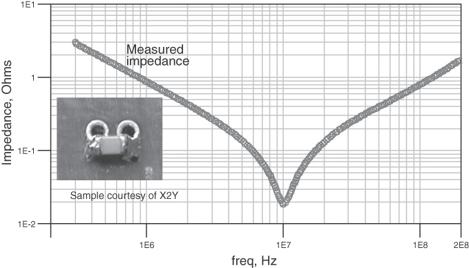
Some capacitors are capable of achieving lower ESL for the same mounting features by nature of their design. It is not that they have lower intrinsic ESL but that they enable lower mounted inductance because of design features. For example, an X2Y capacitor, a type of interdigitated capacitor, will have a lower ESL under typical mounting conditions than an 0603. Figure 13-26 compares the measured impedance profile of an 0603 capacitor and an X2Y capacitor on the same board.
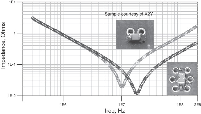
Figure 13-26 Measured impedance profiles of a conventional 0603 capacitor and an X2Y interdigitated capacitor on the same board. They have exactly the same value of capacitance, seen at low frequency, but very different ESL.
The impedance at low frequency for these two different capacitors is nearly the same, but their high-frequency impedance is very different. This is primarily due to the fact that the single X2Y capacitor with four terminals is really like four separate capacitors in parallel. The parallel combination of their loop inductances reduces the equivalent loop inductance of the whole capacitor. This can be a significant advantage in some designs.
The complete path of the power and return currents from the pads of the BGA package to the capacitor is shown in Figure 13-27. The ESL of the capacitor is, to first order, related to design features in this path.

The ESL associated with the capacitor and its path to the package can be divided into four regions:
1. The loop inductance of the surface traces and top of the plane’s cavity
2. The loop inductance of the vias from the capacitor pads to the top of the plane cavity
3. The spreading inductance from the capacitor vias to the vias of the BGA
4. The loop inductance from the cavity under the package to the leads or solder balls of the package
TIP
Different design techniques should be applied to each region in order to engineer the lowest ESL possible.
When only a few capacitors are used on a board, and the current distributions in the planes from the capacitors to the pins of the package do not substantially overlap, the ESL of each capacitor is the loop inductance of the entire path. In this case, each capacitor behaves independently, and it is possible to accurately simulate the impedance profile of the parallel combinations of the capacitors on the board by using a simple SPICE model and simulation. The capacitors are independent.
However, when the current distributions overlap, such as when the capacitors are clustered in one region of the board or when many capacitors surround a package, the spreading inductance in the cavity of the power and ground cavity will be a complicated function of the location of the capacitors, their values, and the location of the package pins.
This is why it is useful to separate the ESL of a capacitor into the mounting inductance and the spreading inductance in the cavity. When the capacitors do not interact with each other, the cavity spreading inductance can be combined with the mounting inductance into the ESL. When the capacitors’ spreading inductances interact, the only accurate way of estimating the impedance profile seen by the package is with a 3D simulator, which takes into account the current distribution of each capacitor. In this case, the location of the capacitors and the location of the power and ground pins in the package will be important.
TIP
It’s always a good practice to separate the mounting inductance and the cavity spreading inductance. They can be combined when needed into one number to estimate the ESL.
13.14 Approximating Loop Inductance
There are only a few geometries for which there are simple approximations for loop inductance:
• Any uniform transmission line
• The special case of two round rods
• A pair of long, wide conductors with a thin dielectric between them
• The special case of edge-to-edge connections to planes
• Spreading inductance from a via to a distant ring
• Spreading inductance between two via contacts in a plane
The loop inductance of any uniform transmission line, assuming that the signal and return paths are shorted at the far end, is given by:
where:
Lloop = loop inductance, in nH
Z0 = characteristic impedance, in Ohms
TD = time delay of the transmission line, in nsec
Len = length of the transmission line, in inches
v = speed of light in the material, in inches/nsec
When the impedance of the line is 50 Ohms, such as a surface microstrip trace that is 10 mils wide and dielectric spacing in FR4 to the return path of 5 mils, the loop inductance is roughly:
For a surface trace that is 0.2 inches long, the loop inductance of the surface trace can be as large as 1.7 nH.
This simple relationship suggests the two important design guidelines for engineering the lowest loop inductance possible for any structure that sort of looks like a uniform transmission line:
• Design the lowest a characteristic impedance possible.
• Keep the lengths as short as possible.
A special structure for which there is an analytical relationship between the geometry and loop inductance is two round rods, as illustrated in Figure 13-28.

The loop inductance from the end of one rod, down the rod, shorting across the end of the other rod and back again to the front is related to only the three geometry terms in Figure 13-28. If the length is increased, the loop inductance will increase. If the rods are brought closer together, their partial mutual inductance will help to cancel some of the total field lines, and the loop inductance will be reduced. If the diameter of the rods is increased, the loop inductance will be decreased.
There are a number of analytical approximations for the loop inductance of these two rods. The simplest approximation is:

where:
Lloop = loop inductance, in pH
h = length of the rods, in mils
s = center-to-center pitch of the rods, in mils
D = diameter of each rod, in mils
For example, for 2 vias, 10 mils in diameter, on 50-mil centers and 100 mils long going through an entire board, the loop inductance is roughly:

The uniform transmission-line model gives the same constant loop inductance per length for the two rods, independent of the rod length. For the case of 10-mil via diameter and 50-mil centers, the loop inductance per pair-length is roughly 23 nH/inch, or 23 pH/mil. When the center-to-center pitch is 40 mils, typical of high-density BGAs, the loop inductance per length is 21 nH/inch, or 21 pH/mil.
TIP
As a rough rule of thumb, if you want to carry around one value for the loop inductance of a pair of vias, a rough estimate is about 21 pH/mil. This is a reasonable estimate for the loop inductance contribution from vias.
When the two conductors that make up the loop are wide and closely spaced, such as with two plane segments shown in Figure 13-29, the loop inductance is approximated by:

where:
Lloop = loop inductance between the planes, in pH
Len = length of the planes, in inches
w = width of the planes, in inches
h = thickness between the two planes in mils

For example, if the planes are 2 inches long and 0.5 inches wide, with 4 mils between them, the loop inductance would be:

When the length of the trace is equal to the width, the structure looks like a square, and the ratio of Len/w is always 1. The loop inductance of this square section of plane is the first part of the equation and is called the loop inductance per square, or the sheet inductance:

Any square piece of a pair of planes has the same loop inductance. The thinner the dielectric between them, the lower the sheet loop inductance.
This approximation assumes that the currents flow in a uniform sheet down the top trace and back to the bottom, uniformly distributed along both sheets. When the contacts are spread along the edge of the strip, this is a good approximation. However, in via contacts to planes, the current does not flow uniformly. Instead, it spreads out from sources and constricts into sinks. An example of the current flow map in a plane between two via contacts is shown Figure 13-30.

Figure 13-30 Current flow pattern in the top plane from a via source point to a via sink point into the bottom plane. Simulated with HyperLynx.
The spreading inductance in planes is the most important property of planes and is discussed in detail in Chapter 6. It contributes to the additional loop inductance between point contacts in planes over their sheet inductance when contacts are at vias rather than at an edge of the plane.
The narrow contact regions of vias increase the current density and increase the local loop inductance. In general, spreading inductance is complicated to calculate and usually requires a 3D field solver, as the current flow is difficult to calculate by approximation.
There is one special case for which there is an accurate approximation for spreading inductance. This is the case of current flowing from a central-ring contact to an outer, symmetrical-ring contact, where it flows into the bottom plane and then reverses back, constricting to an inner ring contact on the bottom plane. This is diagrammed in Figure 13-31.

Figure 13-31 Inner and outer contact regions on the top plane, with similar regions on the bottom plane. Spreading inductance calculation is the loop inductance from the top contact point, radially outward to the edge, down the edge, and back in to the center contact.
In this geometry, the loop spreading inductance is:

where:
Lspread = loop spreading inductance between the planes, in pH
a = radius of the inner contact region, in inches
b = radius of the outer contact region, in inches
h = thickness between the two planes, in mils
This assumes that the current is flowing from the center via contact to the bottom plane and returns to the inside edge of the clearance hole, and the clearance hole is just slightly larger than the via contact diameter in the bottom plane. For example, if the inner radius is 5 mils, corresponding to a 10-mil-diameter via, and the outer radius is 1 inch, corresponding to the perimeter of a package, and the dielectric thickness between the planes is 10 mils, the loop spreading inductance is:

This relationship of spreading inductance has the same form as the sheet loop inductance of a path, if we use as the number of squares:

then:

For typical cases, b/a could be on the order of 100, and the number of squares is of order 1.
In the special case of the current flow between the via contacts to a buried plane pair from a capacitor and BGA pins on the surface of a board, the loop inductance is more complicated to calculate. There are no exact analytical equations that describe this loop spreading inductance. However, by making a few assumptions, a simple approximation can be developed for the loop inductance in a pair of planes with round contact points.
Figure 13-32 illustrates the example of two via contacts positioned a distance B apart in a pair of planes and the current flow between them, spreading out and constricting in the planes.

Figure 13-32 Spreading current from one via contact to another via contact in a pair of planes. There is spreading loop inductance between the two locations.
The spreading loop inductance between these two via contacts is approximated by:

where:
Lvia−via = loop spreading inductance in the planes between the two via contacts, in pH
h = dielectric thickness between the vias, in mils
B = distance between the via centers, in mils
D = diameter of the vias, in mils
For example, if the via diameters are 10 mils and they are spaced 1 inch apart, in a pair of planes with h = 10 mils, the spreading inductance in the planes between the contacts is about:

The contribution of the spreading inductance in the planes between the vias can be as much as 1 nH. The thinner the dielectric, the lower the spreading inductance.
The lower spreading inductance in ultra-thin laminates is the real reason they offer a performance advantage over conventional FR4 for the dielectric between power and ground planes. The higher capacitance plays little role as there is far more capacitance in the on-die capacitance than in the power and ground planes.
If the connections between the capacitors and the pads of the package can be routed in planes with a cavity thickness that is not 4 mils but 1 mil or 0.5 mil, the spreading inductance in this path can be reduced from 0.4 nH with 4 mils down to 0.05 nH with a 0.5-mil-thick dielectric. An example of the cross section of a board with a 0.5-mil-thick dielectric in the power and ground planes is shown in Figure 13-33.

Figure 13-33 Cross section of a board with a 0.5-mil-thick layer of DuPont Interra HK04 laminate between the power and ground planes, close to the bottom surface of the board.
The predicted values of this approximation can be compared to the results predicted by a 3D field solver. Figure 13-34 shows the estimates of these approximations to the simulated via to via spreading inductance using the HyperLynx PI tool for two planes separated by 3 mils.

Figure 13-34 The comparison of the approximation (solid lines) and the simulated loop inductance (single dots), using HyperLynx for the case of a pair of planes separated by 3 mils.
These various approximations can be used to roughly estimate the impact of physical design features and the resulting ESL of a capacitor mounted to a board. Using these approximations, we can explore design space to determine what general design guidelines to follow.
TIP
Since each design is custom, care must be taken when applying an observation for one case and blindly applying it to another without putting in the numbers.
13.15 Optimizing the Mounting of Capacitors
The three most useful approximations for loop inductance are summarized in one place in Figure 13-35.

These approximations describe the important design trade-offs. If you want to reduce the loop inductance associated with the traces from the pads of the capacitor to the vias, there are three important design knobs to adjust:
1. Keep the depth to the top of the power/ground cavity thin.
2. Use wide surface traces.
3. Keep the length of the surface traces short.
To reduce the inductance of the vias, there are three design knobs to adjust:
1. Keep the depth to the top of the power/ground cavity short.
2. Use large-diameter vias.
3. Keep the via pitch as close as possible.
To reduce the spreading-loop inductance in the planes, there are three knobs to adjust:
1. Keep the dielectric thickness of the power/ground cavity thin.
2. Use large-diameter vias or multiple vias in contact to the cavity.
3. Place the capacitor close to the package it is decoupling. (This is only a weak dependence.)
While these are important design guidelines to be aware of, some are more important than others.
TIP
The terms that affect the total loop inductance the most should always be optimized first.
These are the terms that affect the total loop inductance the most:
1. Keep the depth to the top of the power/ground cavity short.
2. Keep the dielectric thickness of the power/ground cavity thin.
3. Use wide surface traces.
4. Keep the length of the surface traces short.
The other design features are of second- and third-order importance and can sometimes be a distraction from the first-order concerns. In general, the only way to know what is important is to put in the numbers for specific cases. Integrating these approximations in a spreadsheet allows us to easily explore design space and identify what is really important and what is not.
In the example shown in Figure 13-36, three cases are explored. In each case, an 0603 capacitor is supplying current to one power and ground pin pair in a BGA package, located some distance away. The vias are 13 mil in diameter. This estimate is for the ESL of the capacitor as though it were not interacting with other capacitors. Case 1 is the starting place, with long and narrow surface traces. The total ESL is found to be about 6.1 nH.

Figure 13-36 Analysis of three typical mounting geometries for an 0603 capacitor, analyzed with an online tool at www.beTheSignal.com.
In case 2, the surface traces are shortened and widened. The resulting ESL is 3.7 nH. Finally, in case 3, the capacitor is moved closer to the package, and the cavity thickness is decreased. The resulting loop inductance is reduced to 1.8 nH.
TIP
This example clearly shows that in typical cases, the loop inductance of the vias is negligible. In most typical cases, especially with thick spacing between the planes, the spreading inductance can be as significant as the surface trace inductance. By careful design of the stack-up, it is possible to routinely achieve less than 2-nH loop inductance.
Surprisingly, the board stack-up plays a significant role in the ESL of the capacitor—in two respects. By moving the top of the cavity closer to the capacitor, the loop inductance of the capacitor and the surface traces is reduced. By making the dielectric thickness of the cavity between the power and ground planes thinner, the spreading inductance is reduced. Adjusting these two design features can bring the ESL from 6 nH to 1 nH in some cases.
Both of these design features are first order and linear in the thickness. Changing via the diameter and moving the capacitor closer to the BGA are log-dependent factors and are of only slight (second- or third-order) importance.
If the surface trace length is also reduced and widened, ESL values as low as 0.5 nH can be achieved. An example of three similar cases is shown in Figure 13-37.

Figure 13-37 Three examples of thin cavity, close to the surface with three different surface traces, resulting in an ESL as low as 0.5 nH, analyzed with an online tool at www.beTheSignal.com.
This model can also be used to assess important design questions such as Is it better to add capacitors under the BGA or on the same surface as the BGA? Figure 13-38 illustrates the two options.

Figure 13-38 Where should the capacitor go: on the same surface as the BGA or directly under the BGA?
Of course, the most common answer to all signal integrity questions is “it depends,” and the only way to get a firm answer is by putting in the numbers.
The right place to put the capacitor is where it will have the lowest loop inductance. Clearly, if the total board thickness is thin, the via loop inductance will be low. If the cavity is far from the surface and thick, the loop inductance of the capacitor on the top will be high. It is possible to find a combination where the top surface capacitor has a much higher loop inductance than the bottom surface capacitor.
However, if the board is thick and the cavity is near the top surface and the cavity is thin, the capacitor on the bottom will have the higher loop inductance. Figure 13-39 summarizes three cases. It shows that placing the capacitor on the bottom can have a loop inductance on the order of 2 nH.

Figure 13-39 Analysis of capacitors on the top and on the bottom of the board. Analyzed with an online tool at www.beTheSignal.com.
If it is possible to achieve lower loop inductance by placing capacitors on the top surface, this is preferred, but as a general rule, if there is the option of doing both, both locations should be used, especially when many capacitors are used in low-impedance applications. When many capacitors are placed around the periphery of the package, their currents can overlap, and the cavity spreading inductance can increase. Placing some of the capacitors under the BGA minimizes the increase in cavity spreading inductance.
TIP
The combination of short, wide surface traces—or via-in-pad technologies—and thin dielectric between the power and ground planes close to the surface can result in typical ESL values from 0.5 to 2 nH. By going to extreme efforts and utilizing interdigitated capacitors, it is possible to achieve loop inductances below 0.5 nH.
If the capacitor mounting inductance is known, based on the design constraints, it will be possible to predict the impedance profile of a collection of capacitors using a 3D field solver. If the mounting inductance changes, as from a stack-up change or a surface-mounting design change, the loop inductance will change, and the impedance profile of the collection of capacitors will change. This is why every PDN design is custom.
TIP
The PDN impedance profile of the combination of capacitors depends very much on the details of the board stack-up, capacitor mounting geometry, and location on the board.
13.16 Combining Capacitors in Parallel
The strategy in engineering the PDN impedance profile is to select the right number and value of capacitors to keep the peak impedance below the target value from where the VRM and bulk capacitors no longer provide low impedance, up to about 100 MHz.
When multiple identical capacitors are connected in parallel, the resulting impedance matches the behavior of an RLC circuit, but the circuit elements values are different.
The equivalent R, L, and C of n capacitors in parallel are:
where:
Cn = equivalent capacitance of n identical real capacitors in parallel
C = capacitance of each individual capacitor
n = number of identical capacitors in parallel
ESRn = equivalent series resistance of n identical real capacitors in parallel
ESR = equivalent series resistance of each individual capacitor
ESLn = equivalent series inductance of n identical real capacitors in parallel
ESL = equivalent series inductance of each individual capacitor
Figure 13-40 shows an example of the impedance profile of multiple identical capacitors in parallel, showing the same general RLC profile but with lower impedance at all frequencies. We are approximating the problem by assuming that the capacitors are independent and their currents do not overlap. The SRF stays the same; it’s the entire impedance profile that scales lower. This is one way of decreasing the impedance profile of a capacitor: Add more of them in parallel.

Figure 13-40 Impedance profile of five identical capacitors added in parallel. With each additional capacitor, the impedance decreases at all frequencies.
However, if the two capacitors have a different value of capacitance or ESL, when they are added in parallel, the behavior is not so simple. Figure 13-41 shows the impedance profiles of two different capacitors with the same ESL and the same ESR. The behavior of the two capacitors in parallel has the same low-impedance dips at the self-resonant frequencies of the individual RLC models. The larger capacitor has the lower SRF. The smaller capacitor has the higher SRF. They each occur when the impedance of the ideal capacitor matches the impedance of the ideal inductance associated with each capacitor. The SRF seen in the parallel combination of capacitors is the same as each individual capacitor’s.

Figure 13-41 The impedance profile of two RLC circuits in parallel, with the same R and L values but different C values. Superimposed is the impedance of the two ideal capacitors and the ideal L and ideal R of both capacitors.
In addition, there is a new feature between the self-resonant frequencies: a peak in the impedance, called the parallel resonant peak, that occurs at the parallel resonant frequency (PRF).
The value of the PRF is difficult to calculate accurately, as it depends on the ESL of the larger capacitor, the C of the smaller capacitor, and the ESR of both of them. If the SRF values are far apart, the PRF is roughly related to:

where:
PRF = parallel resonant frequency, in MHz
C2 = capacitance of the smaller capacitor, in nF
ESL1 = equivalent series inductance of the first capacitor, in nH
For example, if ESL1 = 2 nH and C2 = 10 nF, then the PRF is:
However, when the SRF values are within a factor of 10 of each other, the impedance profile of the parallel combination is distorted from the impedance of the ideal L.The PRF is a more complicated function of the elements, and can more easily be calculated using a SPICE simulation.
TIP
The PRF is one of the most important features of parallel combinations of capacitors because it denotes where there are peaks in the impedance. When few capacitors are used, it’s the parallel resonant impedance that always sets the limit to the PDN performance and must be engineered to lower values.
The peak impedance at the PRF is roughly related to:

where:
Zpeak = peak impedance at the PRF, in Ohms
L1 = equivalent series inductance of the larger capacitor
C2 = capacitance of the smaller capacitor
R1 = equivalent series resistance of the larger capacitor
R2 = equivalent series resistance of the smaller capacitor
This is only approximate and is less accurate as the SRFs of the capacitors are brought closer together. However, it points out the important ways of engineering a reduction in the peak impedance:
• Reduce the ESL of the larger capacitor.
• Increase the capacitance of the smaller capacitor.
• Increase the ESR of both capacitors.
TIP
Where there is the option to use higher-ESR capacitors—referred to as controlled resistance capacitors—they should be considered. A low enough ESR should be selected so that the equivalent ESR of all the capacitors in parallel is just below the target impedance.
The ESR of a capacitor is related to the structure of the parallel plates that make it up and the metallization between the layers. In general, the higher the capacitance, the more plates in parallel and the lower the ESR. Looking at the specifications of a variety of 0402 capacitors can provide a simple generalization for the series resistance of capacitors by capacitor value. Figure 13-42 shows the plotted ESR for various capacitor values, taken off the AVX data sheets.

From the specified ESR, it is possible to derive a simple empirical relationship between the ESR and the capacitance of a capacitor. One empirical approximation is given by:
where:
ESR = equivalent series resistance of the capacitor, in mOhms
C = capacitance of the capacitor, in nF
This simple model is compared with the specified values of ESR in Figure 13-42, and the agreement is seen to be very good.
This suggests that it may be possible to select for higher ESR and lower parallel resonant peak heights if smaller-value capacitors are used. This is especially true when one of the capacitors is the power and ground cavity’s capacitance.
Another important design feature to engineer to decrease the peak impedance value is decreasing the ESL of the larger capacitor or increasing the capacitance of the smaller capacitor. Figure 13-43 shows the impact on the peak impedance as the ESL of the larger capacitor is changed from 10 nH down to 0.1 nH.

Figure 13-43 Impedance profile of a 100-nF and a 10-nF capacitance with ESL of 3 nH in parallel while changing the ESL of the larger capacitor from 10 nH down to 0.1 nH. As the ESL is reduced, the peak impedance drops.
In this example, the larger capacitor is 100 nF, and the smaller one is 10 nF, with an ESL of 3 nH. As the ESL of the larger capacitor is reduced from 10 nH, the peak impedance at the PRF decreases until the SRF of the larger capacitor matches the SRF of the smaller capacitor, in which case there is no peak.
TIP
Reducing the ESL is a significant method of reducing peak impedances.
Unfortunately, due to the complex interactions of the circuit elements, it is not possible to do a simple and accurate analytical analysis of the features of the impedance profile of multiple capacitors. This is especially true as more capacitors are added. Instead, it is critical to use SPICE for such analysis. Luckily, there are many free versions of SPICE readily available on the Internet that can routinely perform this sort of analysis. For examples of these tools, visit beTheSignal.com.
In addition to reducing the ESL of the capacitors to bring the peak impedance values down, there is another way of reducing the peak impedances: Add more capacitors. These can be identical capacitors, or they can be different value capacitors. Both approaches can work.
13.17 Engineering a Reduced Parallel Resonant Peak by Adding More Capacitors
When two capacitors with different SRFs are added in parallel, they create a parallel resonant peak impedance between their self-resonant dips. The peak impedance can be reduced by adding a third capacitor with an SRF between them. What is the optimum value of the SRF of the third capacitor?
The optimum SRF of the third capacitor to give the lowest peak impedance depends on the capacitance values, the ESL values, and the ESR values of all three capacitors. It is difficult to evaluate without a SPICE simulation. There are two obvious algorithms to choose from: Select the third capacitor so that its SRF matches the PRF, or select its SRF so that it is midway between the two other capacitors’ SRFs. The choice depends on the ESL values of the capacitors, their ESR values, and how far apart are the capacitances. Consider the simple case of two capacitors, a 10-nF capacitor and a 100-nF capacitor, both with the same ESL of 3 nH. When combined in parallel, they have a PRF at 21 MHz.
Option 1 is to add a capacitor with its SRF at 21 MHz. The capacitance value is given by:

where:
C3 = capacitance of the third capacitor to be added, in nF
ESL = 3 nH, assumed to be the same for each of the three capacitors
21 = SRF required to match the PRF, in MHz
Option 2 is to select the value of the third capacitor so its SRF is midway (on a log scale) between the SRFs of the other two capacitors. Since their ESL values are the same, this translates to a capacitance of the third capacitor that is the geometric mean of the other two:
Figure 13-44 shows the resulting simulation of the original combination of two capacitors and the impedance profile of the three capacitors, with the value of the third capacitor chosen based on the two options.

Figure 13-44 Comparing the two options for selecting the third capacitor value. The approach that gives the lowest peak impedance is Option 2: Choose the geometric mean.
This example illustrates that when the ESL of the capacitors is the same, the lowest peak impedance can be engineered by choosing a third capacitor that is the geometric mean of the other two capacitors. This is why it is often recommended to select capacitor values spread over a decade scale. If the values are distributed uniformly in a log scale, they will provide the lowest peak impedance.
The only way to know the optimum capacitor values that result in the lowest peak impedances, given the ESL and ESR values, is with a SPICE simulation. When the SRF values for the two capacitors are far apart, using a third capacitor with an SRF near the PRF may be a better choice.
TIP
Whenever different-value capacitors are brought together in parallel, there will always be parallel resonant peaks that must be managed. This will occur at low frequency with the bulk capacitors and at high frequency with the capacitance of the planes and the on-die capacitance.
13.18 Selecting Capacitor Values
Many application notes recommend that all you need to do is add three capacitors per power and ground pin in the package. Half of them recommend using all three capacitors the same value, and the other half of them recommend using different capacitor values. Which is right? The only way to tell is to put in the numbers.
Figure 13-45 compares the impedance profiles for three capacitors all with the same value of 1 µF and three capacitors with values of 1 µF, 0.1 µF, and 0.01 µF. In each case, the ESL is the same 3 nH, and the ESR is chosen based on the values specified by the manufacturer.

Figure 13-45 Impedance profiles for the case of three capacitors, each with a different value, and the case of three capacitors all having the same value.
At first glance, the conclusion would be that the three capacitors all with the same value give the lowest impedance, but, at 100 MHz, the impedance limit they both set is the same, at about 0.6 Ohm. However, this analysis neglects two important effects: at the low-frequency end the interaction with the VRM and bulk capacitor and at the high-frequency end the interactions with the planes of the board, or the on-die capacitance and package lead inductance.
The argument for using three different capacitor values is often that they produce very low impedance at specific frequency regions. While this is true, it’s totally irrelevant. What’s important in the PDN is not how low the impedance profile goes but how high it goes. Peaks in the impedance profile cause failures, and the PDN should be designed to handle this.
Dips in the impedance profile from self-resonant frequencies of capacitors are irrelevant. Peaks in the impedance profile cause failures and are therefore important. The PDN should therefore be engineered to control peaks.
The resulting impedance profiles for these two sets of capacitors, a VRM with a bulk decoupling capacitor and the planes for a board 5 inches on a side and 4 mils thick, is shown in Figure 13-46.

Figure 13-46 The parallel resonances at the boundaries cause peak impedances in both combinations of capacitors.
TIP
At the low frequency, the interactions of the bulk capacitor and the small ceramic capacitors cause the impedance peak at about 1 MHz. The peak impedance is primarily due to the inductance of the bulk capacitor and the capacitance of the MLCC capacitors.
An important way to drop this peak down is to reduce the inductance of the bulk capacitors. In this example, it was assumed to be 15 nH, typical of an electrolytic capacitor. If this can’t be reduced by design, one way it can be dropped is by adding more capacitors in parallel. As long as their SRF is lower than the peak impedance at roughly 1 MHz, their ESL in parallel with the electrolytic capacitor will reduce the peak impedance.
The minimum capacitance needed can be found from a simple estimate. If we assume that we use a tantalum capacitor, with an ESL on the order of 5 nH, in order to have SRF < 1 MHz, the condition is:

By adding an additional capacitor of more than 5 µF and less than 5 nH ESL, the peak impedance at low frequency can be reduced. The precise value of the capacitance is not important; the ESL value is important.
The new impedance profile with a 10 µF tantalum capacitor added is shown in Figure 13-47. The high-frequency impedance peak is created by the interactions of the capacitance of the planes and the ceramic capacitors. The capacitance in a pair of planes is:

Figure 13-47 Impedance profile with an additional 10-µF bulk decoupling capacitor added with an ESL of 5 nH, reducing the peak impedance at low frequency to under 0.1 Ohm.
where:
Cplanes = capacitance in the planes, in nF
Dk = dielectric constant of the laminate materials, typically 4 for FR4
A = area of the planes, in square inches
h = dielectric thickness, in mils
For example, in this case with A = 5 inches × 5 inches = 25 square inches and h = 4 mil and Dk = 4, the capacitance of the planes is:
The parallel resonant frequency is expected at roughly:

The simulated PRF is 70 MHz.
The peak impedance at the PRF is related to the inductance of the capacitors and the capacitance of the planes. In this case, the inductance of the three capacitors is identical, independent of the value of their capacitance. This is why the peak impedance is exactly the same whether we use three capacitors of the same value or three capacitors with different values.
This peak impedance limits the PDN impedance at the board level to about 10 Ohms. If no worst-case current amplitudes are near 70 MHz, this impedance peak may not be a problem. But if you are designing the PDN assuming that you need a target impedance below 10 Ohms, this peak impedance needs to be brought down.
There are six ways of reducing the peak impedance for frequencies below 100 MHz:
1. Increase the capacitance in the planes a lot to push its SRF to very low frequency with a lower peak impedance.
2. Decrease the capacitance of the planes so the PRF is well above 100 MHz.
3. Reduce the inductance of the decoupling capacitors.
4. Increase the ESR of the capacitors.
5. Adjust a capacitor value so its SRF is closer to the PRF.
6. Add an additional capacitor with an SRF near the PRF.
We rarely can adjust the capacitance of the planes. It is what it happens to be. One of the reasons all PDN designs are custom is that the plane capacitance will vary depending on the board size and stack-up. This will shift the PRF over a wide range of frequencies.
TIP
Reducing the ESL of the bulk capacitors should always be at the top of the list of actions. Everything should always be done to reduce the ESL. Selecting lower-value-capacitance capacitors may provide higher ESR and more damping.
If we are limited to using just three capacitors, it may be possible to find a value of one of the capacitors so that its SRF is closer to the PRF of the planes. This would reduce the peak impedance by a closer SRF and by a higher ESR, increasing damping.
We would want to adjust the third capacitor, C3, so that its SRF is close to the PRF. The condition is:
This reduces to:
Figure 13-48 shows the impedance profile of the capacitors, VRM, and planes with the third capacitor changed from 10 nF to 2 nF.

Figure 13-48 Impedance profile with the 10-nF capacitor changed to 2 nF with a lower peak impedance.
TIP
It is counterintuitive that by decreasing the capacitance of one of the capacitors, the impedance profile actually improves. By optimizing the capacitor value, we reduce the peak impedance from 10 Ohms down to 2.5 Ohms. This reduces the PDN noise by four times in the 50-MHz to 100-MHz range.
Which is better: three capacitors all with the same value or three capacitors with different values? If you randomly select the three capacitor values or blindly use values of 1 µF, 0.1 µF, and 0.01 µF, then it probably doesn’t matter which approach you choose. They each have the same chance of success or failure. However, if you can optimize the capacitor value to minimize the peak impedance at the PRF with the plane’s capacitance, using different-value capacitors results in a lower peak impedance profile.
In this example, the lowest peak impedance that could be obtained below 100 MHz using just three capacitors, even if their values are optimized, is still limited to about 2 Ohms. This can be dramatically improved with more capacitors.
13.19 Estimating the Number of Capacitors Needed
In the absence of more detailed information, the goal of the board-level PDN design is to engineer the impedance peaks below the target value up to about 100 MHz, or roughly where the package limits the impedance that the chip will see, which could be at lower frequency.
At the low-frequency end, the number and values of the bulk capacitors can be adjusted to keep the peak impedances below the target value.
At the high-frequency end, the absolute lowest maximum impedance a collection of capacitors can theoretically have is set by their parallel combination of equivalent series inductance. The best case is if there is no parallel resonance with the plane’s capacitance, and all the inductances are in parallel. The design condition is that:
where:
Zcapacitors = impedance of the capacitors in parallel, in Ohms
Ztarget = target in impedance, in Ohms
Fmax = highest frequency where the board-level impedance can play a role
If the impedance of the capacitors at the high-frequency end is all due to the parallel combination of inductances and they all have the same value of ESL, this condition translates to:

where:
Ztarget = target in impedance, in Ohms
Fmax = highest frequency where the board-level impedance can play a role, in GHz
ESL = equivalent series inductance of each capacitor, in nH
n = number of capacitors needed in parallel to meet the target impedance
This establishes the theoretical minimum number of capacitors needed in parallel to meet this impedance target as:

For example, if the target impedance is 0.1 Ohm and Fmax is 100 MHz and each capacitor has 2 nH of ESL, then the theoretical minimum number of capacitors needed is:

TIP
In order to reduce the number of capacitors needed, regardless of their value, the ESL must be reduced. This is why ESL is such an important number.
Figure 13-49 shows how the theoretical minimum number of capacitors varies based on the ESL and the target impedance.

Figure 13-49 Minimum number of capacitors required to achieve a target impedance at 100 MHz based on an ESL value.
The minimum number of capacitors possible to achieve a target impedance is a good figure of merit to evaluate how well optimized a design might be. This would be the case when the PDN is not delivering power to a Vdd core but providing a low impedance for return currents, for example. More capacitors in parallel would act as shorting inductors to reduce the impedance of the power and ground planes with a DC block.
In the example in the preceding section, we achieved a target impedance of 2 Ohms with three capacitors, each with an ESL of 3 nH. The theoretical minimum number that could be used, as shown in the chart in Figure 13-7, is one. Using three to get there is not very efficient due to the complication of the PRF of the planes.
13.20 How Much Does a nH Cost?
The cost of a small ceramic decoupling capacitor is almost negligible. Its largest direct costs are in the assembly operation and in the indirect costs of more vias to drill, the surface real estate taken up, the potential of blocked routing channels, and the impact on the board layer count.
Using a rough estimate of $0.01 for the total direct material cost and assembly cost per capacitor, we can estimate how much an nH is worth. For every fraction of a nH reduction in the ESL, fewer capacitors need to be used, and there is a direct cost savings.
The cost per nH is derived from the expression above for the theoretical minimum number of capacitors needed:
This is displayed in Figure 13-50 for different ESL and target impedance values for a maximum frequency where the board plays a role of 100 MHz.

The cost per nH can be estimated based on:

where:
TotalCost/ESL = cost per nH, in $/nH
Fmax = highest frequency at which the board-level impedance can play a role, in GHz, assuming ~ 0.1 GHz
Ztarget = target impedance, in Ohms
This is a simple result. It suggests that the lower the target impedance, the more expensive every nH becomes and the more valuable a reduction in the ESL becomes.
For example, with a target impedance of 0.01 Ohm, the cost per nH is $0.6/nH. If the mounted inductance is 2 nH, the total cost of the capacitors is about $1.20 for the board. If the ESL can be reduced from 2 nH to 1 nH just by changing the surface traces or bringing the power and ground plane cavity closer to the board surface, the cost savings from the reduction in the number of capacitors used would be $0.60, with no sacrifice in performance. If this were a high-volume board, with 1 million units per month, the cost savings would be $600k per month, or $7.2 million per year.
The contribution of spreading inductance for the planes is roughly:

where:
Lvia−via = loop-spreading inductance in the planes between the two via contacts, in pH
h = dielectric thickness between the vias, in mils
B = distance between the via centers, in mils
D = diameter of the vias, in mils
For a typical case of B = 1 inch and D = 10 mils, the spreading inductance in the planes is roughly about:

When a conventional thickness of 4 mils is used, the spreading inductance contribution is on the order of 0.4 nH per capacitor. If an ultra-thin laminate, such as the DuPont Interra HK04 material, with a thickness of 0.5 mils, were used, the spreading inductance would be on the order of 0.05 nH. This is a reduction of about 0.35 nH and translates into a potential cost reduction of:

When the cost reduction is greater than the cost premium for the thinner dielectric, using the more expensive ultra-thin laminate becomes a reduction in the total cost of ownership. The premium is rated as an extra price per square foot of board area, or:

If the premium were about $3/square foot extra cost, then the condition for total cost reduction with a thin laminate would be:
where:
CostReduction = cost reduction in the number of capacitors not needed, in $
Ztarget = target impedance, in Ohms
Premium = added cost per square foot of thin laminate over conventional laminate, in $/square foot
area = area of the board surface in the specific application, in square feet
If the area is described in square inches, this relationship becomes:
This suggests that if the board area is 10 square inches, a thinner laminate is a cost reduction if the target impedance is lower than 0.01 Ohm.
13.21 Quantity or Specific Values?
To first order, the impedance at high frequency of a collection of capacitors is related to the parallel combination of their inductance. However, if a parallel resonance with the capacitance of the board planes exists near the maximum frequency where the board impedance plays a role, it will artificially increase the impedance profile of the capacitors. In this regime, the impedance of the collection of capacitors can be brought down by carefully selecting the values of capacitor to “sculpt” the impedance profile and compensate for the parallel resonance.
The impact from the parallel resonance on the impedance profile for a collection of capacitors is illustrated in Figure 13-51 for the specific case of:
Ztarget = 0.1 Ohm
Fmax = 0.1 GHz
ESL = 2 nH
n = 13 capacitors
A = 65 square inches and 6.5 square inches

Figure 13-51 Impedance profile of 13 capacitors interacting at high frequency with the 65 and 6.5 square inches of board capacitance, compared to the impedance of the ideal inductance of 13 capacitors. Top: PRF = 100 MHz; bottom: PRF = 3 × 100 MHz.
In this example, the theoretical minimum number of capacitors needed to achieve the 0.1 Ohm at 0.1 GHz is:

When the PRF is close to the Fmax, it artificially increases the impedance profile of the capacitors and the planes’ capacitance. This increase can be more than a factor of two or three.
However, if the PRF can be engineered to be a higher frequency—by decreasing the area of the planes, for example—the parallel resonance does not interact with the impedance of the capacitors near the Fmax, and the impedance can be close to the theoretical impedance of the n inductors in parallel. In this case, achieving the target impedance at the Fmax with the minimum number of capacitors does not depend on the specific value of capacitors; it just depends on their number and their ESL.
The PRF of the capacitors’ inductance interacting with the planes’ capacitance is given by:
where:
PRF = parallel resonant frequency, in MHz
n = number of capacitors in parallel
ESL = equivalent series inductance of each capacitor, in nH
Cplanes = capacitance of the planes, in nF
h = dielectric thickness between the planes, in mils, assuming Dk = 4
A = area of the planes, in square inches
The goal is to engineer conditions so that the PRF is pushed to frequencies above the maximum frequency. To first order, this would suggest:
• Large n
• Thicker h
• Small ESL
• Small A
However, the dielectric thickness also affects the ESL. Increasing h will increase ESL. Given the importance of lower ESL, thinner h is usually better. To push the PRF to a high enough frequency where it is not interacting with the impedance of the capacitors, it needs to be at least three times higher than the max frequency.
The condition for the specific values of the capacitors to not be significant is roughly approximated, as illustrated above, to be:
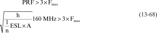
In addition, if the number of capacitors is adjusted to meet the target impedance at the maximum frequency, a further condition is:
These two relationships can be combined to result in the condition where the impedance at Fmax is independent of the specific values of the capacitors selected as:

where:
n = number of capacitors in parallel
Ztarget = target impedance, in Ohms
A = area of the planes, in square inches
Fmax = highest frequency where the board-level impedance is important, in GHz
ESL = equivalent series inductance of each capacitor, in nH
h = dielectric thickness between the planes, in mils, assuming Dk = 4
For the best conventional case of h = 4 mils and the typical Fmax of 0.1 GHz, this condition reduces to:
where:
Ztarget = target impedance, in Ohms
A = area of the planes, in square inches
TIP
This suggests that to engineer a condition where the values of the capacitors are not important and where it is still possible to use the theoretical minimum number of capacitors, the area of the power planes should be kept to a minimum and the target impedance low.
In general, the area of the planes is always less than the area of the board. When split planes are used, the actual board area can be more than a factor of three larger than the power planes. If well engineered, the area of the power plane can be kept to a minimum to support all the capacitors and connections to the VRM. When power planes are mixed on signal layers as copper fill areas, the small power planes are sometimes referred to as a copper puddle.
TIP
Whenever split planes are used, it is always important to keep signal layers from crossing underneath them. Signal layers crossing under split planes has the potential of generating noise in the power plane and excessive coupling between adjacent signal lines.
In many applications with dedicated power planes, the plane area and board area may be close. This design space is mapped in Figure 13-52.

Figure 13-52 Design space of when the capacitor values selected are important and when they are not important for the special case of dielectric thickness of 4 mils.
For this specific case of a dielectric thickness of 4 mils, if the target impedance is 0.1 Ohm, then as long as the area of the planes is less than roughly 7 square inches, the selection of capacitor values is not important. They can all be the same value.
If, however, the plane area is larger than 7 square inches, the capacitance of the board will push the PRF close to 0.1 GHz and increase the impedance of the combination of capacitors. In this case, to use the minimum number of capacitors, their value is important and should be selected to “sculpt” the impedance profile.
This design space of target impedance higher than 0.1 Ohm and plane area larger than 7 square inches encompasses many boards. In this regime, to use the smallest number of capacitors and achieve the lowest cost, the precise values of capacitors should be carefully selected. Their values and number are chosen to bring the peak impedances below the target value up to the maximum frequency.
This is why for many common board applications, using a distribution of capacitor values will enable the lowest impedance with the fewest capacitors rather than all the same value of capacitance. Of course, the minimum number of capacitors is based on using the right distribution of values.
If the plane area can be kept to less than 2 square inches, then all designs with a target impedance less than 0.3 Ohm can use the same value capacitors and the minimum number of capacitors. This is a rather small plane area and not very common. However, the package is about this size.
TIP
The package can act as a small board. If enough capacitors are added to the package, the impedance may be reduced to the level where the impedance of the board is not important.
While there is rarely enough on-package decoupling capacitance to supplement all the board-level needs, it is possible to add all the necessary capacitors using a small size interposer rather than in the package. Such an alternative approach is available from Teraspeed Consulting Group.
An example of a small island of low-impedance power and ground provided in the PowerPoser is shown in Figure 13-53. This small board fits underneath the package and has multiple layers of thin laminate with all the very low inductance decoupling capacitors to bring the impedance below the target value from low frequency to very high frequency.

Figure 13-53 The role of the PowerPoser in a board stack-up and a close-up view of an FPGA chip mounted on a PowerPoser.
By using an interposer, very thin dielectric layers near the surface can be used without paying a large-area price penalty, and low inductance capacitors can be placed in proximity to the package. The area of the planes can be kept small so the parallel resonant frequency is well above the package limit, and all capacitor values can be the same.
13.22 Sculpting the Impedance Profiles: The Frequency-Domain Target Impedance Method (FDTIM)
Parallel resonances in the PDN cause impedance peaks, which ultimately are the source of failures in the PDN. These parallel resonances are caused by a parallel combination of a capacitor and an inductor—somewhere.
In the case of the Vdd supply, as viewed by the pads of the die, the capacitor is the on-die capacitance, and the inductor is the package lead inductance. It’s this parallel resonance that can cause excess Vdd noise. At the board level, the best we can achieve is a flat impedance response, which will damp this parallel resonance.
The impedance of the power and ground plane cavity, as seen on the board, is important for signal-return-path noise and noise coupling from the planes to other components. This noise is also related to peaks in the cavity PDN. This is primarily from the parallel resonance between the cavity capacitance and the equivalent-series inductance of all the MLCC capacitors in parallel.
The solution for this PDN is to reduce the total parallel inductance and reduce any peaks. Both of these problems can be minimized by engineering a PDN profile that is flat, without significant peaks.
By optimizing the values of the capacitors, a flat impedance profile can be engineered with the smallest number of capacitors. In this design regime, it is possible to minimize the number of capacitors used to achieve the target impedance by careful selection of their values. This process is called sculpting the impedance profile.
TIP
No matter what, it is always important to use the lowest possible ESL for all decoupling capacitors. This will always result in the smallest number of capacitors and the lowest-cost system.
The precise number and optimized values of capacitors needed will depend on:
• The bulk decoupling capacitors associated with the VRM
• The capacitance in the board
• The target impedance
• The maximum frequency
• The ESL of each capacitor
The combination of these terms varies dramatically from product to product, so it is not possible to give one capacitor distribution that will always work. However, the methodology can be applied to many designs.
This methodology was pioneered by Larry Smith while he was at Sun Microsystems and has been termed the Frequency-Domain Target Impedance Method (FDTIM). The process leverages the simulated impedance profile of a collection of capacitors, including their ESL and ESR, with the capacitance in the planes at high frequency and the bulk capacitors associated with the VRM at the low-frequency end.
Capacitor values are selected from the values available from vendors. Not all values are available; rather, the common values are in decade steps of multiples of 1.0, 1.5, 2.2, 3.3, 4.7, and 6.8. When the ESL of each capacitor in a collection is the same, the minimum parallel resonant impedance peak is obtained when each capacitor value is the geometric mean of the capacitor on either side of it.
The optimum distribution would be using values of decade multiples of 1, 2.2, and 4.7, for example. The largest capacitance value of an 0402 capacitor easily available is about 1 µF. When higher values are needed, a 1206 capacitor can provide as much as 100 µF.
The lowest-value capacitor needed is about ⅓ × the capacitance in the planes. The board capacitance is on the order of 10 nF for a board with 40 square inches, for example. The smallest-value capacitor needed would be about 2.2 nF.
The selection of possible values might range from 1 µF to 2.2 nF and may include nine different values from which to select:
1000 nF
470 nF
220 nF
100 nF
47 nF
22 nF
10 nF
4.7 nF
2.2 nF
A typical set of parameters might be:
• 50 square inches of board area with ~20 nF of capacitance
• Target impedance of 0.1 Ohm
• ESL of 2 nH for each capacitor
• Maximum frequency of 0.1 GHz
In this example, the board area of 50 square inches and target impedance of 0.1 Ohm puts the design in the upper part of the design space, where the value of the capacitors matters. Of course, if the target impedance were low enough or the board capacitance were small enough, it would not matter what value capacitors were used; they could all be 1 µF. In that case, parallel resonances would not play a role.
The theoretical minimum number of capacitors required to meet the target value for the above condition is:

where:
n = minimum number of capacitors needed
Fmax = highest frequency for board-level impedance, in GHz
ESL = equivalent series inductance of the capacitor, including the mounting inductance and some of the cavity spreading inductance, in nH
Ztarget = target impedance, in Ohms
Starting at the low-frequency end, the largest capacitor value is selected and simulated. Enough capacitors of each value are added to bring the peak impedance below the target value. Capacitors are added, along with enough quantity of this value, until the target impedance is reached. Specific capacitor values are skipped, especially at the low-frequency end, where the low target impedance can be reached without them. The ESR for each capacitor value is used in the simulation.
Figure 13-54 shows an impedance profile based on the following capacitor selection with a total of 14 capacitors:
C |
n |
470 |
1 |
100 |
1 |
47 |
1 |
22 |
1 |
10 |
3 |
4.7 |
3 |
2.2 |
4 |
Total |
14 |

Figure 13-54 Impedance profiles for two distributions of 14 capacitors. One distribution uses all 1-µF capacitors. The other distribution was chosen to sculpt the profile. At 100 MHz, the sculpted profile meets the target impedance, but the other distribution does not.
In Figure 13-54, the impedance profile meets the target impedance up to 100 MHz, using 14 capacitors. This is close to the theoretical minimum of 13. However, using 14 capacitors all with the same value of capacitance is not able to achieve the same low impedance. If all the same value capacitors were used, more than 14 would be required. It would not be as low a cost as using the FDTIM.
TIP
Of course, if any of the initial conditions of this specific problem were changed—for example, if the ESL were not 2 nH but really 3 nH—this combination would no longer work.
Figure 13-55 shows the impedance profile for these capacitors with an ESL of 3 nH, exceeding the target impedance at a number of frequencies. This is another example of the importance of reducing the ESL for capacitors and how custom the selection of capacitors becomes when so many system parameters affect the impedance profile.

Figure 13-55 Impedance profile for the same distribution of capacitor values as in Figure 13-54 but each with an ESL of 3 nH rather than 2 nH.
TIP
Of course, there are many right distributions. The most cost-effective solutions use a total number of capacitors that is close to the theoretical minimum.
Another example of a sculpted-impedance profile for a target impedance of 0.05 Ohm is shown in Figure 13-56. In this case, the theoretical minimum with an ESL of 2 nH is 26. This distribution used 33, slightly above the theoretical minimum. The capacitor values used were:
C |
n |
1000 nF |
1 |
470 nF |
1 |
220 nF |
1 |
100 nF |
1 |
47 nF |
2 |
22 nF |
3 |
10 nF |
5 |
4.7 nF |
6 |
2.2 nF |
13 |
Total |
33 |

13.23 When Every pH Counts
The four most important design “habits” to follow are:
1. Use the shortest and widest possible surface trace that is consistent with the assembly design rules. In other words, use as few squares of surface interconnect between the capacitors and the vias as possible.
2. Place the capacitors in proximity to the package—some below it on the bottom side of the board and some on the same layer—to avoid saturating the spreading inductance with all peripheral capacitors.
3. When power and ground planes are on adjacent layers, use the thinnest possible dielectric that does not cost extra. This is usually 2.7 to 4 mils, depending on the vendor.
4. When possible, place the power and ground cavity as close to the surface of the board as possible.
There is rarely a reason not to do these habits, and they will always result in lower ESL.
The cost impact for an ESL reduction is:

When the target impedance is 0.1 Ohm or higher, this is less than $0.06 per nH per voltage rail on a board. There usually isn’t enough cost savings potential to justify paying extra for low-inductance features. However, when the target impedance is 0.001 Ohm, the cost savings is $6/nH for each voltage rail on the board. Every pH reduction is a half-cent cost reduction.
TIP
The lower the mounting loop inductance of each capacitor, the fewer capacitors are required to achieve the low target impedance at the high frequency. Every free option should be used to reduce the ESL of all decoupling capacitors.
As pointed out earlier in this chapter, sometimes paying extra for thinner dielectric between the power and ground planes is worth the extra cost of the lower spreading inductance.
In addition, alternative capacitor technologies can offer a lower mounted ESL than conventional capacitors. Most capacitors are designed with their terminals along their long axis. The capacitor body is a minimum of two squares. Even with via-in-pad, there are still two squares of surface trace.
An alternative design uses reverse aspect ratio capacitors, with terminal pads along the long side of the capacitor. Mounted onto a board, these capacitors could be implemented with as low as 0.5 square. An example of these capacitors is shown in Figure 13-57.

Figure 13-57 Capacitor technologies. Left: Conventional-aspect-ratio capacitors with minimum number of surface trace squares of n = 2. Right: Reverse-aspect-ratio capacitors available from AVX, with a minimum n = 0.5.
If the depth in the board stack-up to the power and ground cavity is 5 mils below the top surface, the sheet inductance of surface traces would be about 32 pH/mil × 5 mil = 160 pH/sq. The trace loop inductance of a via-in-pad, best-case standard capacitor is about 320 pH, while for a reverse-aspect-ratio capacitor, the best case could be as low as 160 × 0.5 = 80 pH. This is a reduction of 240 pH.
Interdigitated capacitor technologies can offer even lower capacitance. These are constructed as multilayer ceramic capacitors with multiple interleaved terminals on each end. Examples are illustrated in Figure 13-58.

An IDC is effectively multiple capacitors in parallel, with the ESL of each current path in parallel. The equivalent ESL of the four capacitors in one IDC would be one-quarter the ESL of any one of them. In addition, since the current flow is in opposite directions in adjacent capacitor segments and they are in close proximity, the effective ESL of each one is further reduced. An IDC can have less than 20% the ESL of a conventional capacitor.
Another type of IDC is provided by X2Y Attenuators. These are multilayer ceramic capacitors with alternating plates coming out to each of four different electrode terminals. An example of these four-terminal capacitors and their internal structure is shown in Figure 13-59.

Figure 13-59 Examples of X2Y capacitors and their internal structure, as described by X2Y Attenuators.
The A and B plates are both connected in parallel to the power plane, while the central two G1 and G2 plates are connected in parallel to ground. In this configuration, the capacitor behaves like four capacitors in parallel, with current flows illustrated in Figure 13-60.

Figure 13-60 X2Y capacitor mounted to a circuit board with the top and bottom terminals tied to power and the two central terminals tied to ground. It behaves like four capacitors in parallel.
While there are similar performance advantages using either IDC technology, an advantage of the X2Y capacitors is the ease of integration with conventional through-hole circuit board technology.
An 0805 IDC with four terminals on a side will have a pad footprint with 20-mil centers between pads. This is difficult to connect to circuit boards using conventional through-hole technology and requires via in pad. An 0805 X2Y capacitor can use via holes on 40-mil centers, as shown earlier in this chapter, and can use conventional through-hole technology, leaving a routing channel through the holes available for multiple 5-mil-wide tracks.
The combination of IDC, minimum surface trace size, and cavity close to the surface can enable a total ESL from the capacitor to the package pin of less than 250 pH.
However, if the surface traces are long and the cavity is not near the surface, the same X2Y capacitor can show an ESL that is more than 1 nH—three times larger than it needs to be—just from very slight design variations. Figure 13-61 shows an example of the measured impedance profile of two X2Y capacitors with the comparison of an RLC model.

Figure 13-61 Measured impedance profile for two X2Y capacitors mounted to a test board with slightly different conditions. The measured data is compared to the simulated impedance of an ideal RLC circuit. The insets show the capacitor for each measurement.
For each capacitor RLC model, the same value of C = 180 nF was used in the model, the same value of R = 0.013 Ohm was used, but two different inductance values were used. For the best case, L = 260 pH gave an excellent fit, while for the other case, L = 900 pH was the best fit. The peaks near 200 and 300 MHz are the parallel resonances with the circuit board to which the capacitors were mounted.
When every pH counts, the right capacitors and the optimum mounting inductance can make all the difference.
13.24 Location, Location, Location
At low frequency, below the parallel resonant frequency of the capacitors’ ESL and the planes’ capacitance, the planes will interact with the capacitors as a lumped element. However, when the length of an edge of the planes is comparable to a fraction of the wavelength, the resonant behavior of the board will show up in the impedance profile.
When the probe point is located at the edge of the board, the first resonant frequency will be when:
Len = length of an edge of the board, in inches
λ = wavelength of light where the first resonance shows up, in inches
Dk = dielectric constant of the laminate between the planes
c = speed of light in air, 12 inches/nsec
fres = resonant frequency, in GHz
v = speed of light in the material, assumed v = 6 inches/nsec, for FR4
For example, if the board is 10 inches on a side, the first resonance will be about 300 MHz. If the probe point is in the middle of the board, the first resonance will be at twice this frequency, or 600 MHz.
Figure 13-62 is an example of the simulated impedance profile of a 10 inch × 10 inch bare board, probed in the center, showing the capacitive behavior at low frequency, its self-resonant frequency, and the onset of board resonances at 600 MHz.

Figure 13-62 Impedance profile of a bare board, showing the onset of board resonances at 600 MHz. Simulated with HyperLynx 8.0.
While the board will appear as a lumped capacitor below the resonant frequency, and a simple SPICE simulation will accurately reflect the impedance profile of the capacitor on the board, the spreading inductance the capacitor sees between its location on the board and the device it is decoupling will depend on location.
The farther away the capacitor is from the package it is decoupling, the higher its total ESL due to the spreading inductance. When the spreading inductance is small compared to the mounted inductance of the capacitor, the location is not important. Changing the capacitor position will change the spreading inductance, but this will have minimal impact on the total ESL of the capacitor.
TIP
However, when the spreading inductance is a significant fraction of the total capacitor’s ESL, the location will have a significant impact on the ESL of the capacitor, and moving the capacitors closer to the device is important.
The condition for when location is important is based on the amount of spreading inductance compared with the mounted inductance of the capacitor. The condition is:
When spreading inductance ~ mounting inductance, location matters.
When spreading inductance << mounting inductance, location does not matter.
For a via about 10 mil in diameter and a capacitor 1 inch away, the spreading inductance is roughly:

When h is thin, spreading inductance is small, and location is important only for very low values of mounting-inductance capacitors.
When h is thick, spreading inductance is larger. When the mounting inductance of capacitors is low, location can be important. Due to the very rough approximate nature of the spreading-inductance estimate, when the spreading inductance is on the same order as the mounting inductance, it is appropriate to use a 3D field solver tool to estimate the impact on the impedance profile of the mounted capacitors from location.
Figure 13-63 shows an example of the impedance profile of two board configurations. In each case, the same four capacitors are mounted to the board, close together. The mounting inductance of each is 5 nH, so the four of them have an equivalent inductance of 1.25 nH.

Figure 13-63 Simulated impedance of four capacitors mounted to a 30-mil-thick cavity and a 4-mil-thick cavity located close to the package pin and far from the package pin. Simulated with HyperLynx 8.0.
In the first example, the cavity thickness is 30 mils. The spreading inductance is on the order of 3 nH, large compared to the mounting inductance of the four capacitors. The impedance profile of these four capacitors is simulated when they are located far from the package pin and when they are close. The large difference in impedance in these two positions shows the impact from location on the total ESL.
In the second example, the cavity thickness is 4 mils, and the spreading inductance is on the order of 0.4 nH. This is small compared to the 1.25-nH inductance of the capacitors. When the position of the capacitors is changed from near to far, there is little change in the simulated impedance. The spreading inductance is not an important contributor to the capacitor’s inductance, and location is not important.
In low-impedance designs, where the ESL has been optimized to less than 0.25 nH for each capacitor, the spreading inductance can be a significant contributor and should be taken into account with a 3D field solver. The spreading inductance will increase the contribution to the inductances of the individual capacitors in a complicated way that depends on the position of the capacitors and the location of the package pins. It can only be analyzed with a 3D field solver.
13.25 When Spreading Inductance Is the Limitation
For a given target impedance and maximum frequency, the total, maximum allowable series inductance that could be in the path, including the capacitors and plane spreading inductance, must be:
Lmax = maximum allowable series inductance, in nH
Fmax = maximum frequency where board-level impedance is important, in GHz
For example, if the target impedance is 0.01 Ohm and the maximum frequency is 100 MHz, the maximum allowable series inductance before it dominates the impedance of all the capacitors is:
If the total series inductance to the capacitors exceeds 16 pH, the PDN impedance will be higher than the target impedance at the highest frequency the board is effective. If the vias in the board from the package to the planes and the spreading inductance in the planes from the package pins to the capacitors is a large fraction of this inductance, the spreading inductance will limit the impedance of the board.
If the capacitors are uniformly distributed around the package with the power and ground pins also distributed around the perimeter of the package, as shown in Figure 13-64, the spreading inductance in the planes can be estimated.

Figure 13-64 Estimating the best-case spreading inductance in the planes as current flows from the distribution of capacitors to the pins in the package.
The spreading inductance in the planes is approximately:

where:
Lspread = spreading inductance in the planes, in pH
h = dielectric thickness between the planes, in mils
b = distance to the capacitors, in inches
a = radius of the power/ground pins in the package, in inches
For example, if h = 4 mils, b = 1 inch, a = 0.25 inches, then the spreading inductance is:

It is possible that the equivalent inductance of the vias in the board from the package pins may also add to this limiting inductance. If the power and ground cavity is 10 mils below the top surface, there will be about 210 pH per power and ground via. For 10 power and ground pin pairs, this is an equivalent via inductance of 21 pH, comparable to the spreading inductance. The combination may almost double the limiting inductance when the package pins look into the board to the capacitors.
TIP
The vias in the board to the cavity and the spreading inductance in the cavity to the capacitors can easily dominate the impedance of the collection of capacitors when the target impedance is below 0.05 Ohm.
Based on the root cause of the spreading inductance, there are only a few board-level design features that can be engineered to reduce it:
• Use thinner dielectric layers between the planes.
• Use multiple planes in parallel.
• Move the power and ground cavity closer to the top of the board.
• Spread the capacitors farther out around the perimeter of the package. This has a limit once the capacitors are uniformly distributed around the perimeter.
• Mount some of the capacitors under the package on the bottom of the board.
Some design features can be implemented in the package design if planned ahead of time including the following:
• Mount some of the capacitors within the ring of the power and ground pins of the package.
• Spread the power and ground pins of the package to the outer perimeter of the package.
• Add decoupling capacitors on the package.
• Use more power and ground pin pairs in parallel.
Figure 13-65 shows an example of adjusting the chip attach footprint of the package to allow decoupling capacitors inside the power/ground ring of pads.

Figure 13-65 Package attach footprint of an Altera Stratix II GX FPGA, showing the capacitor attach pads around the periphery and inside the BGA footprint.
When spreading inductance limits the series inductance, the worst thing to do would be to cluster the capacitors or cluster the power and ground pins into the core region of the package.
Because of the 3D nature of the current flows in the planes, the only way to accurately estimate the series inductance contribution from the planes, given the capacitor locations and power pin locations, is with a 3D field solver.
13.26 The Chip View
Through most of this chapter, we have considered the impedance profile seen by the board. Once the board-level impedance is designed, what impact does this have on the chip-package combination?
In the following example, the conditions are:
• Target impedance of 0.01 Ohm
• Fmax of 100 MHz
• Board area of 25 square inches
• h of 4 mils
• ESL per capacitor of 1 nH
• On-die capacitance of 250 nF
This combination puts us in the regime where the precise capacitor values don’t matter, and they can all be the same value. However, where possible, the lowest value of capacitors should be used so that the capacitors have the highest possible ESR and contribute to damping of parallel resonances. The theoretical minimum number of capacitors needed is:

The maximum allowable spreading inductance to the package would be:
As we saw above, it would be impossible to achieve this with a conventional BGA package and 4-mil-thick layers with the capacitors on the top surface. The capacitors would have to be attached under the BGA, and the laminate thickness would have to be reduced or multiple planes would need to be added to the board. Only a 3D field solver would be able to confirm that these modifications provided low enough spreading inductance.
Given these modifications, the board-level decoupling can be achieved with 63 0402 1 µF capacitors, each with an ESL below 1 nH.
What will the chip see? Figure 13-66 shows the impedance profile from the board level and the chip level for this condition.

The low-frequency impedance is optimized by designing the VRM and bulk decoupling capacitors. The board impedance is set by adding 63 MLCC capacitors to achieve the 0.01-Ohm impedance up to 100 MHz. This meets the condition for an optimized board-level PDN design.
However, as viewed by the chip pads, looking through the package into the board, the on-die capacitance and the series package pin inductance and capacitor equivalent inductance create a parallel resonance that results in a large impedance peak near 80 MHz in this case. As with any other parallel peak impedance, it is composed from a capacitance sloping down and an inductance sloping up. An important term that affects the peak impedance is the equivalent series resistance of the parallel resonant circuit.
One important driving force for using a flat impedance profile on the board to which the package and on-die capacitor are attached is that it acts as a damping resistance to reduce the peak height. Using the FDTIM, the capacitor values can be selected to engineer a flat-impedance profile. If this flat region extends under the chip-package parallel resonance, it will damp the peak as seen by the Vdd pads on die. This is not the only way to provide damping resistance, but it can be an effective method.
If the FDTIM is not used, but all the capacitor values are the same value, there will still be some damping series resistance from the parallel combination of the ESR of the capacitors and the series resistance in the package leads and on the die itself.
When the equivalent series resistance is low, the peak impedance can be high. For capacitors near 1 µF, their ESR is on the order of 10 mOhms. With 63 in parallel, the equivalent resistance is reduced to about 0.0002 Ohm, well below the target impedance level. If 10 nF capacitors were used, their ESR would be about 70 mOhms each, with a total series resistance about 0.001 Ohm. This is better than using all higher values of capacitors, but it is still not enough to damp out the parallel resonances. The series resistance of the package traces will be below 0.001 Ohm. This results in a series resistance that might be dominated by the on-die metallization.
TIP
The resistance from on-die interconnects is an important term that can be used to engineer a lower peak impedance.
Figure 13-67 shows the impact that different on-die resistance can have. The resistance is changed from 1 milliOhm, to 3 milliOhms, and 10 milliOhms. It has to be lower than 10 mOhms to meet the target impedance spec, but some on-die resistance is a good thing.

Figure 13-67 The impact on the impedance profile as seen by the chip, from different on-die series resistance in the PDN.
Even if the on-die resistance is optimized, the peak impedance at the parallel resonance will still be above the target. This is where on-package decoupling capacitors can play a role in suppressing the peak impedance.
Figure 13-68 shows the impact on the impedance profile the chip sees looking into the PDN as the number of on-package decoupling capacitors is increased from none to 10. Each has an ESL of 0.1 nH, which is typically implemented using IDC.

Figure 13-68 The impedance profile seen by the chip as 3, 6, 8, and 10 on-package decoupling capacitors are added.
In this example, when 10 IDC, each with an ESL of 0.1 nH, are added to the package, the impedance profile seen by the chip is as shown in Figure 13-69, meeting the 0.01-Ohm target impedance from DC to very high bandwidth.

13.27 Bringing It All Together
The most important feature of the PDN is how low it keeps the voltage noise on the pads of the chip. This is fundamentally related to the current draw of the chip and the impedance profile from the chips’ pads to the VRM. Unfortunately, this depends very strongly on factors that are often beyond the control of the board-level designer, such as:
• Current spectrum drawn by the chip operations
• On-die capacitance
• On-die resistance
• Chip attach inductance
• Package attach inductance
• On-package decoupling capacitors
In the highest-performance systems, where the target impedance is in the milliOhm range—such as for high-end processors, servers, and graphics chips—system co-design, simultaneously optimizing the chip features, package features, and board features, is critically important for a robust, cost-effective design.
TIP
Companies that implement system-level PDN design will end up being the most successful.
But for most designs, there is nothing the board-level designer can do about the chip or the package. It is limited by the semiconductor provider. While it is always important to continue to push the envelope and ask for the chip and package models to incorporate in the board-level PDN design, it is rarely possible to get all the important information required.
The board-level designer is faced with having to follow the guideline that “sometimes an okay answer now is better than a good answer later” and base the board-level PDN design on reasonable assumptions.
If enough on-package decoupling capacitance is provided, the requirements for on-board decoupling can be dramatically reduced. For example, in the earlier example, the 10 on-package decoupling capacitors provide an equivalent inductance of 1/10 × 100 pH = 10 pH. This interacts with the on-die capacitance to keep the peak impedance below the target impedance in the 100-MHz region and above.
This inductance is on the chip side of the interconnects, between the package and the board. The equivalent package-attach inductance to the board could be large and may not affect the high-frequency impedance the chip sees. In fact, it could be as large as 0.1 nH. This is illustrated in Figure 13-70.

Figure 13-70 Impedance profile the chip sees with on-package capacitors providing the low impedance at high frequency and changing the package-attached inductance from 0.05 nH, to 0.1 nH, and 0.15 nH.
If the package inductance is 0.1 nH, the highest frequency at which the board can affect the impedance the chip sees is:

Ztarget = target impedance, in Ohms
Lpkg = inductance of the package attach to the circuit board, in nH
Fmax = highest frequency at which the board-level impedance can affect the chip-pad impedance, in GHz
The use of package-level decoupling capacitors and higher package attach inductance can mean that the requirements for the board-level decoupling are reduced. If the maximum target impedance is no longer 100 MHz but 16 MHz, fewer capacitors are required to meet the same impedance level. Of course, the same considerations about parallel resonance peak impedances at the interfaces must be taken into account. Figure 13-71 shows that using the lower-ESL capacitors on package can reduce the number of board-level capacitors required from 63 to 15 and still meet the target impedance.

Figure 13-71 Impedance that the profile chip sees with on-package capacitors and reducing the board-level capacitors from 63 to 15 while still maintaining the impedance target.
TIP
When there are on-package capacitors, the board-level requirements can be reduced. Even then, selecting the capacitors is not about the capacitor value but about the ESR and ESL they provide.
When semiconductor vendors incorporate on-package decoupling capacitors, they often specify the recommended board-level decoupling requirements in terms of how many capacitors and what value should be added to the board. This is rarely useful information, as the number of capacitors to add to the board is not about their capacitance but about their ESL.
13.28 The Bottom Line
1. PDN design is confusing, contradictory, complicated, and complex. This is fundamentally due to the complex interactions of many features that are beyond the control of the board designer and that are often poorly documented.
2. The goal of the PDN is to provide a low impedance from the chip pads to the VRM.
3. The VRM and bulk-decoupling capacitors provide low impedance at low frequency.
4. Do everything possible to integrate the bulk capacitors with low loop inductance.
5. The chip and package design have the most influence on the impedance in the 100 MHz and above region. The most important design guidelines are to add more on-die decoupling capacitance, to keep the chip-attach inductance low, and to add low-inductance decoupling capacitors to the package.
6. The most important starting place in PDN design is establishing a target impedance. This can be approximated based on the worst-case power consumption of the device.
7. The package lead inductance and circuit board via to the power/ground cavity will fundamentally limit the high-frequency design for the board-level impedance.
8. At the board level, everything possible should be done to reduce the loop inductance from the capacitors to the packages.
9. The most important design guidelines are to use power and ground planes on adjacent layers, with thin dielectric, placed close to the surface of the board; to use short and wide surface traces between the capacitors and their vias to the cavity; and to place the capacitors in proximity to the package on the top surface and, when spreading inductance is saturated, to place some directly beneath the packages on the bottom of the board.
10. The most important terms that influence the number of capacitors to use is their ESL and the maximum frequency for the board-level decoupling.
11. When the board planes’ capacitance creates a parallel resonance with the decoupling capacitors at a low frequency, you can use the smallest number of capacitors by carefully selecting their values using SPICE to simulate the impedance profile.
12. For very low-impedance designs, the values of the capacitors are not as important as their ESL and the number used. All the same value capacitors can work well.
13. When parallel resonant peaks are involved, the lowest-capacitance capacitors will have the highest ESR and provide some damping to reduce the peak impedance.
14. For very low impedance, on-package capacitors are essential. Their use may decrease the on-board capacitor requirements.
15. For the very lowest-impedance PDN designs, co-design of the chip, package, and board-level PDN will provide the best cost–performance solutions.
End-of-Chapter Review Questions
13.1 What are five elements that are part of the PDN?
13.2 What are two examples of interconnect structures that are not part of the PDN?
13.3 What are three potential problems that could arise with a poorly designed PDN?
13.4 What is the most important design principle for the PDN?
13.5 What performance factors influence the target impedance selection?
13.6 What are the three most important design guidelines for the PDN?
13.7 A 2-V power rail has a ripple spec of 5% and draws a maximum transient current of 10 A. What is the estimated target impedance?
13.8 What is one downside to implementing a PDN impedance that is well below the target impedance?
13.9 Why is the PDN easier to engineer by looking in the frequency domain?
13.10 What are the five frequency regions of the impedance of the PDN in the frequency domain, and what are the physical features that affect it?
13.11 What feature in the PDN provides the lowest impedance at the highest frequency?
13.12 What is the only design feature you need to adjust to reduce the impedance at the highest frequency, and why is this difficult to achieve?
13.13 What are the three most important metrics that describe a VRM?
13.14 What is the key SPICE element that enables simulation of an impedance analyzer?
13.15 Why is reducing the package lead inductance so important?
13.16 A 2-layer BGA has leads that run from one side to the other side. If adjacent power and ground leads are 0.5 inches long, and there are 20 pairs, what is the equivalent package lead inductance of the PDN?
13.17 What package style would have the lowest loop inductance? What three package features would you design to reduce the package lead inductance?
13.18 Why is it sometimes noticed that if you take off all the decoupling capacitors on a board, the product will sometimes still work? Why is this not a good test?
13.19 What are the three most important features of an MLCC capacitor, and what physical features affect each term?
13.20 Why is reducing inductance in the PDN elements on a board so important?
13.21 What are the three most important design guidelines for reducing the mounting inductance of an MLCC capacitor?
13.22 What three design features will reduce the spreading inductance in a power and ground cavity, and which is the most important?
13.23 In what combination of design features will the position of a decoupling capacitor not be important? In what case is location important?
13.24 A capacitor really does not behave like an ideal capacitor on a board at the higher frequencies. What is a more effective way of thinking of a capacitor?
13.25 A surface trace on a board from a capacitor to the vias to the cavity is 10 mils wide and 30 mils long. The top of the cavity is 10 mils below the surface. What is the mounting inductance of the 0603 capacitor? What would be the loop inductance of the vias if they were 10 mils in diameter?
13.26 What happens to the self-resonant frequency when 10 identical capacitors are added to a board? What are the features that change?
13.27 What new impedance feature is created when two different-value capacitors are added in parallel? Why is this a very important feature for PDN design?
13.28 What are three design guidelines for reducing the parallel peak impedance between two capacitors?
13.29 What happens to the ESR of a capacitor as the value of the capacitance increases?
13.30 To reduce the number of capacitors needed to achieve a target impedance, what is the most important design feature to adjust?
13.31 What is one advantage of engineering a flat PDN impedance profile?
13.32 What is the FDTIM process and why is it a powerful technique?