
Appendix D. Review Questions and Answers
This appendix contains review questions and answers to help you solidify your understanding of the material covered throughout the book. Try to answer all questions before looking at the answers that follow.
Chapter 1
1.1 Name one problem that is just a signal-integrity problem.
Reflections on a transmission line are just a signal-integrity problem. This is sometimes called “self-aggression” noise from the signal in the transmission line.
1.2 Name one problem that is just a power-integrity problem.
The rail noise on the core’s Vdd supply on the die is just a power-integrity problem. This is also an example of “self-aggression” noise on the Vdd rail, as it comes from the noise on the Vdd rail from the currents in the Vdd rail.
1.3 Name one problem that is just an electromagnetic compliance problem.
The source of ALL radiated emissions is from changing currents in extended conductors which are part of the system. Of course, the source of the currents is only from either signal and return currents or from power or ground currents, so there is always interaction between these three effects. However, many features of signals that do not affect the signals can have a dramatic impact on EMI. One good example is a slight mode conversion in a differential pair, such as a CAT 5 twisted pair. A small amount of common signal on the twisted pair will have no impact on the differential signal, but can cause a complete EMC failure.
1.4 Name one problem that is considered both an SI and PI problem.
The most commonly occurring problem that involves both signals and power integrity is ground bounce. This is the effect in which there is a skewed-up return path—i.e., not a wide uniform plane, and there are signals that share this common return path. When the return path is a narrow path like a lead in a package, it will have more inductance than a wide plane.
Since signal return paths are typically shared by power return paths, the skewed-up return paths could be part of the signal interconnects, or part of the power distribution network. When current flows through this shared, common return path, a voltage is generated. This is “ground bounce.” It is a form of cross talk between signals, or cross talk between power and signals.
1.5 What causes an impedance discontinuity?
An impedance discontinuity occurs when the instantaneous impedance the signal would see changes. This happens whenever the cross-sectional geometry changes. This could be when the signal conductor changes shape, when the return path geometry changes, or both. Discontinuities usually happen at interfaces of structures—from on-die, to packages, to traces on one layer, thru vias, and through connectors.
1.6 What happens to a propagating signal when the interconnect has frequency-dependent losses?
Generally, losses from conductors and dielectrics increase as you go up in frequency. When a signal with a fast edge passes through an interconnect with losses increasing with frequency, the higher frequency components will be attenuated more than the lower frequency components. This effectively decreases the bandwidth of the signal.
A high bandwidth signal will have a short rise time. As its bandwidth decreases, the rise time will increase. This rise time increase is the chief problem with lossy interconnects. When the rise time is comparable to the unit interval of the data pattern, the losses will affect signal quality.
1.7 What are the two mechanisms that cause cross talk?
The fundamental mechanism for cross talk is fringe electric and fringe magnetic field coupling. If all the electric and magnetic fields between the signal and return paths were confined to the vicinity of the signal paths, there would be no cross talk.
We can approximate the electric and magnetic field coupling as circuit elements with coupling capacitance and coupling inductance, which are called mutual capacitance and mutual inductance.
1.8 For lowest cross talk, what should the return path for adjacent signal paths look like?
A wide, solid plane always confines the stray electric and magnetic fields more than any other structure. For the lowest cross talk, always use a wide return plane. Any other structure increases the relative cross talk.
1.9 A low-impedance PDN reduces power-integrity problems. List three design features for a low-impedance PDN.
The power distribution network (PDN) are all the interconnects from the pads of the VRM to the pads of the power rail on the die. One way of reducing the impedance is by reducing the loop inductance in the path. This would be by 1) bringing the power path as close as possible to the ground path, 2) keeping interconnects short, and 3) using wide conductors like planes.
To reduce the interconnect lengths between the planes and the devices, 4) the power and ground planes should be on adjacent layers 5) with a thin dielectric, and 6) positioned as close as possible to the top component layer in the stack up.
1.10 List two design features that contribute to reduced EMI
One of the biggest sources of EMI is common currents on external, twisted pairs, like CAT 5 cables. This is reduced by using a shielded cable like CAT 6, with its shield connected to the chassis. It’s not that the “shield” in anyway shields the fields inside from radiating. It’s that the shield acts as a return path for the common currents on the twisted pair and reduces the external fields from the common currents.
A second problem arises from the connection of the shield. If it is not a 360-degree connection and does not look like an ideal coaxial connection, there will be some total inductance in the return path. When return current flows through this total inductance, it generates a ground bounce voltage and drives new common currents on the outside shield of the cable.
1.11 When is it a good idea to use a rule of thumb? When is it not a good idea to use a rule of thumb?
The starting place for tackling any problem should be applying a rule of thumb to estimate what to expect. This initial value will help drive your engineering judgment. When you are ready to sign off on a design, when the accuracy of the value to 10% or better is important, do not use a rule of thumb—use a numerical simulation with a verified process.
1.12 What is the most important feature of a signal that influences whether it might have a signal-integrity problem?
All signal-integrity problems increase with shorter rise time. Generally, when the rise time of a signal is 10 nsec or longer, the interconnects are pretty transparent and signal-integrity problems will be small. But, as the rise time decreases, signal-integrity problems will get worse. Generally, if the rise time is 1 nsec or less, interconnects are not transparent; and if you don’t worry about signal integrity, your product probably will not work the first time.
1.13 What is the most important piece of information you need to know to fix a problem?
The root cause. If you don’t know the correct root cause, your chance of fixing a problem is based on pure luck. Not only must you know the root cause, but you must have confidence you have the correct one. This is usually by thinking of as many consistency tests as you can, and trying them.
1.14 Best design practices are good habits to follow. Give three examples of a best design practice for circuit board interconnects.
1. Route all signals as uniform transmission lines.
2. Avoid using branches when routing signal lines.
3. Always use a continuous return path under each signal line.
4. Consider using a termination if the line is long enough or rise time short enough.
5. Always use as short a surface trace as possible for capacitors so their mounting looks as close to via in pad as practical.
6. Avoid messing up return paths or overlapping return currents of different signal paths
1.15 What is the difference between a model and a simulation?
A model is the electrical description of a physical structure, component, or device. It is the input information to the simulator, written in the language the simulator understands. For example, for a SPICE-like circuit simulator, the language of models is circuit elements such as capacitors, resistors, inductors, and transmission lines.
A simulator is an engine that computes electric or magnetic fields, S-parameters, voltages or currents in the time or frequency domain. Sometimes an S-parameter description of an interconnect can be used as a behavioral model of the interconnect and inserted in a simulation tool.
1.16 What are the three important types of analysis tools.
The simplest type of analysis tool is a rule of thumb. This is easy to use, but not intended to be very accurate. It’s designed to be the starting place of any analysis and helps establish solid engineering judgment.
The next, more accurate tool is an analytical approximation. While they can sometimes look complicated, this is not measure of their accuracy. They can be integrated into a spreadsheet and what-if scenarios evaluated. Their accuracy is not well established.
The potentially most accurate analysis tool is a numerical simulation. Although the value of this type of analysis can be very high, it also comes at a higher cost in expertise, learning curve, and actual dollar cost of the tool.
1.17 What is Bogatin’s rule #9?
Before you do a measurement or simulation, always anticipate what you expect to see. If you are wrong and you see something that is different than you expected, there is a reason for it. Do not use the result until you can understand why the result is not what you expect. Maybe you did something wrong, or the tool is wrong.
If you are correct, and you see what you expect, you get a nice warm feeling that maybe you do understand what you are doing. It is an important confidence builder.
The corollary to Rule #9 is that there are so many ways of screwing up a measurement or simulation, you cannot do enough consistency tests to help test the quality of your result.
1.18 What are three important reasons to integrate measurements somewhere in your design flow?
The input information to many simulators are material properties. These can often only be obtained from measurements.
The accuracy of models of components can only be validated by measurements.
Many simulation tools are intrinsically accurate. However, the process used to set up the problem and integrate it into the simulation tool may not be done correctly. The best way to validate a simulator tool and process to use it is by comparing the results to measurements on a well-characterized test vehicle.
1.19 A clock signal is 2 GHz. What is the period? What is a reasonable estimate for its rise time?
The period of a 2 GHz clock signal is 1/F = 0.5 nsec. If the rise time is about 10% of the period, the rise time would be 0.05 nsec, or 50 psec. This is just a rough estimate of what fraction of the period the rise time might be. It could be as long as 50% the period.
1.20 What is the difference between a SPICE and an IBIS model?
A SPICE model describes an active device as a combination of voltage and current sources and capacitors, inductors, and resistors. These are circuit element models which can often be related to specific physical features that make up the microscopic model of the device.
An IBIS model of a driver is often described as a behavioral model of the device. It consists of the behavior of the voltage-current curves of the driver under different load conditions. There is no connection between the behavior of the I-V curves and any physical design features.
1.21 What do Maxwell’s Equations describe?
They relate how electric and magnetic fields interact with currents, charges, and each other. Most importantly, Maxwell introduced two important new features in his equations. The first is the idea that a changing electric field acts just like a current, but is not the motion of physical charges. He termed it displacement current. This is a critically important concept in signal integrity.
The second important innovation he introduced in his equations was the coupling between a changing electric field generating a changing magnetic field, which then generates a changing electric field. It’s this mutual interaction that is the origin of propagating electromagnetic fields.
When you combine the linear differential equations between E fields and B fields, you get a linear, second order differential equation in just the E field and just the B field. The solution to these equations are propagating electric and magnetic fields—light.
1.22 If the underlying clock frequency is 2 GHz, and the data is clocked at a double data rate, what is the bit rate of the signal?
With two bits in every clock period, the bit rate would be 4 Gbps. The underlying clock frequency of a data rate, when there are two bits per cycle, is called the Nyquist frequency.
Chapter 2
2.1 What is the difference between the time domain and the frequency domain?
The time domain is the real world. The frequency domain is a mathematically constructed world.
In the real world, events happen sequentially with a time stamp and interval between events. An important property of the time domain in the real world is causality. This means, a response cannot happen before a stimulus.
In the time domain, we describe a signal as a voltage at discrete instants in time. A waveform is a voltage vs time display.
The frequency domain is a mathematical construct. In this precisely defined domain, the only type of waveforms that can exist are sine waves. The collection of all the various sine waves in a signal is a spectrum. A signal is then a voltage amplitude and phase at discrete frequency values.
2.2 What is the special feature of the frequency domain and why it is so important for signal analysis on interconnects?
In the frequency domain, the only type of waveform that can exist is a sine wave. Some physical effects have a natural response that matches the shape of sine waves.
This is the case when the physical effects are described by second order, linear differential equations. The solutions for these equations are sine waves. This means sine waves are naturally occurring in such systems.
Electrical circuits with resistors, capacitors, inductors, and transmission lines are described by linear, second order differential equations. This means that sine waves are naturally occurring in electrical circuits.
Many of the voltage vs time responses of electrical circuits will look like combinations of sine waves. Often, these waveforms can be described in a simpler way by just a handful of sine waves in the frequency domain than by voltage vs time in the time domain. When this is the case, you can often have a simpler solution in the frequency domain than in the time domain. This often translates to a shorter time to the answer by passing through the frequency domain than staying in the time domain.
2.3 What is the only reason you would ever leave the real world of the time domain to go into the frequency domain?
Since the real world is in the time domain, your first choice is always to stay in the time domain to solve problems. The only reason you would ever leave the real world to detour through the frequency domain, this mathematically constructed world, is to get to the answer faster.
Not all problems can be solved more quickly in the frequency domain. But when it works, the frequency domain can be an important shortcut. This is why you should become bilingual and learn to think and act in both the time domain and the frequency domain.
2.4 What feature is required in a signal for the even harmonics to be nearly zero?
In a time-domain waveform that is repetitive, each harmonic in the frequency domain will be a multiple of the repeat frequency. If the waveform is symmetric—that is, whatever happens in the first half of the period is exactly the same, with a negative sign in front of it—all even harmonics will have a zero amplitude. There will be no even harmonics in the frequency domain.
However, if there is any asymmetry between the first and second half of the period of the waveform, some even harmonics will appear. For example, if the signal is a square wave with a duty cycle of 50%, there will be no even harmonics. If the duty cycle is NOT 50%, there will be even harmonics.
If the waveform has some features that happen in the first half of the period of the waveform that doesn’t exist in the second half—like a rise time different than a fall time—there will be even harmonics.
2.5 What is bandwidth? Why is it only an approximate term?
The bandwidth of a signal is the highest sine-wave-frequency component that is significant in the spectrum of the signal. This means that you can eliminate all the frequency components of the signal above its bandwidth, and when you re-create the waveform, not have any important impact on the signal.
It is as though you send original signal through a low-pass filter with a steep high-frequency stop at the bandwidth. When you compare the original and filtered signal, they should be the same for all important features you care about.
But the terms “significant” and “care about” are vague terms. If you define the similarity of the original and low-pass filtered waveform as no difference to 10% in voltage vs time or no difference to 1% or no difference to 1%, you will get a different value for the bandwidth.
This makes the term bandwidth an approximate term. If you care about the 1% differences, you should not use the term bandwidth but include the whole signal waveform or the whole spectrum.
2.6 In order to perform a DFT, what is the most important property the signal has to have?
In order for a discrete Fourier transform to be most useful in describing a signal in the frequency domain, you should make sure the signal is repetitive and there are a whole number of cycles within the time window you use to calculate the DFT.
If this is the case, you will see harmonics as multiples of the repeat frequency of the signal and the spectrum will be independent of the number of cycles in the time interval.
If you choose a time interval that does not contain a whole number of cycles, the spectrum that results will depend specifically on the time interval you choose and will not be intrinsic to the signal.
2.7 Why is designing interconnects for high-speed digital applications more difficult than designing interconnects for rf applications?
Signals in high-speed digital applications have a wide bandwidth. This means interconnects must be well-behaved over a wide frequency range. Signals in the rf world have a narrow bandwidth, centered over the carrier frequency. This means interconnects must be well behaved at one frequency, the carrier frequency.
I think it is easier to design an interconnect for specific impedance properties at one frequency than over a wide range of frequencies.
Of course, “easier” is a subjective term. My friends working in the rf world would probably say their designs are harder to engineer than high-speed digital designs because they require much tighter control of impedance and can’t tolerate cross-talk levels that are as high as in digital designs.
2.8 What feature in a signal changes if its bandwidth is decreased?
The bandwidth is like the value of the frequency cliff in the low-pass filter. When selected as the bandwidth of the signal, it will be the lowest frequency at which the original signal and the filtered signal should look the same.
If you send a signal through a low-pass filter, the chief feature in the output signal that changes when you decrease the cliff frequency is the rise time of the signal. The lower the bandwidth, the longer the rise time.
2.9 If there is −10 dB attenuation in an interconnect, but it is flat with frequency, what will happen to the rise time of the signal as it propagates through the interconnect?
It the frequency response of the −10 dB attenuation is flat, this means every frequency component in the spectrum of the signal would see the same attention. The shape of the spectrum would stay the same; it would just be scaled down, everywhere, by −10 dB, which is a drop to about 30% of the original amplitude.
Since the rise time is related to the relative drop from the frequency components in the spectrum and the shape stays the same, the rise time would be the same. The signal amplitude would just be scaled.
Attenuation by itself does not cause rise-time degradation. It’s the frequency dependence of the attenuation that does.
2.10 When describing the bandwidth as the highest significant frequency component, what does the word significant mean?
The term “significant” is a vague term. It refers to the highest sine-wave-frequency component that needs to be included in any analysis. If you set all the frequency components above the bandwidth to zero and convert the signal back into the time domain, all the important properties of the signal you care about, like the rise time, will be preserved and close enough to the original signals.
Describing the bandwidth of a signal is the same as saying if you send the signal through a low-pass filter with a very steep, cliff wall drop-off, what is the lowest wall frequency you could use and still preserve the important features of the signal?
Different applications might have a different meaning of “significant.” If you want to re-create the rise time of a signal, and get the same 10−90 rise time of the signal after it passes through the cliff wall filter, you would need a cliff wall at about 0.35/rise time.
2.11 Some published rules of thumb suggest the bandwidth of a signal is actually 0.5/RT. Is it 0.35/RT or 0.5/RT?
If you are worrying about the difference between 0.35 or 0.5 in the relationship, don’t use the term bandwidth. You should consider the entire spectrum in your analysis. The term bandwidth, when referring to preserving a rise time, is too vague to distinguish 0.35 or 0.5.
If the rise time of the signal is 10% the period, T, of a square wave, for example, the harmonics will be at multiples of 1/T. This means the resolution of looking at the features of the spectrum will be at 1/T.
The bandwidth, defined by 0.35/RT, is the same as saying a frequency of 0.35/(0.1 × T) = 3.5/T. Saying the bandwidth is 0.5/RT is the same as a frequency of 5/T. The resolution of the spectrum is only 1/T and you are trying to distinguish a value of 3.5/T or 5/T. These two values are within 1.5/T of each other, close to the resolution limit of the spectrum.
2.12 What is meant by the bandwidth of a measurement?
The bandwidth of a measurement is the highest sine-wave-frequency component that you can measure in the system of the probes or fixtures and the device. To quantify this value, you usually define the frequency at which the amplitude of the detected signal is reduced by −3 dB of what is actually there.
In many digital storage scope (DSO) applications, the shape of the frequency response curve has a very sharp drop off at the high-frequency end, due to extensive signal processing. It is customary practice to define the bandwidth of the scope instrument alone as the −2 dB frequency point.
A 1 GHz scope has a −2 dB frequency point at 1 GHz. This would be based on sending sine waves into the scope and looking at the highest frequency that gets in with a signal amplitude down by only −2 dB.
A frequency-domain instrument, like a spectrum analyzer or a network analyzer, typically has a flat response, after calibration, up to the highest measurement frequency. Beyond this, the measured response, is, of course, zero. The bandwidth of the instrument is just the highest measured frequency component.
2.13 What is meant by the bandwidth of a model?
The bandwidth of a model is the highest sine-wave frequency at which the model’s predictions matches any measurement of the real components response to an “acceptable” level of accuracy.
Again, this term of “acceptable” is vague. Depending on the application, it generally means an agreement to within 10% between the measured response and the simulated response of the real component.
Generally, the agreement between the measured and simulated response drops off in accuracy much faster above the model’s bandwidth than below the bandwidth.
2.14 What is meant by the bandwidth of an interconnect?
The bandwidth of an interconnect is the highest frequency that can be transmitted through the interconnect and still meet the required signal performance specification.
Obviously, depending on the application, the requirement will change. If you want to preserve the rise time of the signal and not affect it by transmission through the interconnect, this generally means the frequency at which a signal would have an attenuation of −3 dB.
This assumes the attenuation is linearly frequency dependent. If the attenuation were flat at −3 dB, the rise time would not be degraded at all. If the frequency response were a cliff wall low-pass filter, the frequency at which the output 10−90 rise time were the same as the input rise time might be closer to the −2 dB point.
However, if the application required having just −20 dB of the carrier frequency amplitude at the output, compared to the signal at the input, you could tolerate a much poorer interconnect.
This is why you often add a qualifier to the term bandwidth of the interconnect and refer to the −3 dB bandwidth, or the −10 dB bandwidth, or the −20 dB bandwidth. This is based on what an acceptable attenuation might be for the application.
2.15 When measuring the bandwidth of an interconnect, why should the source impedance and the receiver impedance be matched to the characteristic impedance of the interconnect?
If you define the interconnect bandwidth as the highest frequency at which you have −3 dB of the input signal at the output, there are two reasons why the source and receiver impedance matter, compared to the characteristic impedance of the interconnect.
The amount of signal launched into the transmission line depends on the impedance of the source compared to the impedance of the interconnect. Increase the source impedance and less signal is launched into the transmission line. Likewise, change the receiver impedance and the output voltage at the receiver will vary. Increase the receiver impedance, and more voltage will be measured at the receiver.
If the source and receiver impedances are not matched to the characteristic impedance of the interconnect, then the reflections between the ends of the interconnect will cause ripples in the frequency response of the interconnect. These ripples are not intrinsic to the response of the interconnect. You can change their modulation depth by changing the external conditions of the source and receiver impedances.
You will minimize the effects of the terminations at the ends if you match the terminations to the characteristic impedance of the interconnect. This reveals the intrinsic performance of the interconnect.
Of course, if the interconnect is not a controlled impedance interconnect, and its instantaneous impedance varies down its length, there will be reflections inside the interconnect, which are part of the intrinsic properties of the interconnect. The best you can do is match the source and receiver impedances to the average, or low-frequency characteristic impedance of the interconnect.
This is where you sometimes must define the bandwidth of the interconnect at a specific terminated impedance. Luckily, if you know the interconnect response at one termination value, you can mathematically calculate the response at any other terminations. There is no need to measure every combination.
2.16 If a higher bandwidth scope will distort the signal less than a lower bandwidth scope, why shouldn’t you just buy a scope with a bandwidth 20 times the signal bandwidth?
There are two reasons why higher bandwidth isn’t necessarily better. First is cost. The higher the bandwidth of the scope, the more expensive it is. When purchasing an instrument, you always should consider the useful future use, or “headroom” of the instrument, and your budget.
Like hard drive memory space, you should always buy the highest bandwidth you can afford.
There is a fundamental problem with higher bandwidth measurements. Every receiver has some noise associated with it, even if it is just the digitizing noise of the ADC. Generally, the noise density is flat with frequency. This means that a higher bandwidth measurement lets in more amplifier noise than a lower bandwidth measurement. If there is no signal information at the higher bandwidth, all you are doing is increasing the noise.
The signal-to-noise ratio is literally the ratio of the signal energy to the noise energy. If a higher bandwidth measurement does not increase the signal energy, but only increases the noise energy, you get a lower SNR with a higher bandwidth scope.
This is why most scopes have a feature to allow the user to select the measurement bandwidth at the front of the amplifier. If you have plenty of SNR, it may not matter. But if you are pushing the limits to SNR, you want to use just enough measurement bandwidth to let in all the signal, but not so much as to let in more noise in a frequency range where there is no signal.
If you want to be a master of measurements, always pay attenuation to the bandwidth of your signal and match your measurement bandwidth to be at least twice the signal bandwidth so you don’t lose any signal—but not too much above this, so you don’t add too much noise.
2.17 In high-speed serial links, the −10 dB interconnect bandwidth is the frequency where the first harmonic has −10 dB attenuation. How much attenuation will the third harmonic have? How small an amplitude is this?
In an interconnect that is dominated by dielectric loss, the attenuation of the interconnect, in dB, drops off linearly with frequency. If there is −10 dB at a first-harmonic frequency of 1 GHz, for example, the attenuation at the third harmonic, 3 GHz, will be 3× this or −30 dB.
The amplitude of the first harmonic of the signal at the receiver will be down to 30% of the input signal with −10 dB of attenuation. At −30 dB attenuation, the amplitude will be down to:
This is not much signal left at the third harmonic.
2.18 What is the potential danger of using a model with a bandwidth lower than the signal bandwidth?
The whole purpose of a model is to represent the electrical behavior of the actual component. Its value is in how faithfully or accurately it predicts the actual performance of the real component.
The bandwidth of the model is the highest frequency at which the model’s prediction matches the real component behavior. If the signal has frequency components above the model’s bandwidth, the predictions of the model will no longer be accurate. Although you will get an answer, it will be wrong.
If the signal bandwidth exceeds the model’s bandwidth, the answer will be wrong, but it will be very difficult to quantify how wrong is the answer. This can often be misleading either as worse than reality, in which case you end up over-designing the product, or better than reality, in which case you end up with a product that may not work.
2.19 To measure an interconnect’s model bandwidth using a VNA, what should the bandwidth of the VNA instrument be?
At a minimum, the model’s bandwidth should be at least as high as the signal bandwidth, and the instrument’s bandwidth at least as high as the required model’s bandwidth.
If you can afford it, using a model and measurement bandwidth that are 2× the signal bandwidth adds a factor of two margin, which accounts for the vagueness of the term bandwidth. It’s a question of if you can afford it.
In a VNA, the bandwidth of the instrument is very well defined. It is the highest frequency the VNA goes up to. Generally, the cost of a VNA measurement goes up with higher measurement bandwidth. It’s the price of the VNA, and the cables, the connectors, the calibration system, the fixture design, and the care with which the measurements must be performed.
The bandwidth of the VNA to use should be at least as high as the required bandwidth of the model and extend up to the highest frequency you can afford. But going above 2× the model bandwidth does not add any additional value, unless the application requires knowing the limits. If there is no additional value above 2× the model bandwidth, higher frequency measurements than 2× the model’s required bandwidth should be used only if it is free.
2.20 The clock frequency is 2.5 GHz. What is the period? What would you estimate the 10−90 rise time to be?
The period is 1/clock frequency. If the clock frequency is 2.5 GHz, the period is 1/(2.5 GHz) = 0.4 nsec.
Of course, just because you know the period doesn’t mean you have any knowledge of the rise time. You have to make some assumptions. Generally, the rise time is about 10% the period in many clocked digital systems. Using this rule of thumb, if the period is 4 nsec, the rise time would be about 0.1 × 0.4 nsec = 0.04 nsec = 40 psec.
However, this assumption fails at extremes. In high-speed serial links, the rise time is often 1/2 the unit interval. The signal goes up and it goes down in one unit interval. If the unit interval is half the underlying clock frequency, called the Nyquist, the rise time is 0.25 × the clock period.
In simple microcontroller circuits, like the Arduino, the clock frequency is 16 MHz. The period is 60 nsec. You would expect the rise time to be about 6 nsec using the 1/10th rule of thumb. When measured, you find the rise time of signals coming off the I/O to be 3 nsec, half the expected rise time.
But sometimes, an ok answer now! is better than a good answer late. If all you know is the period and you need a rough estimate, not knowing anything else about the system or the signal, using the 1/10th rule of thumb is a good starting place.
2.21 A repetitive signal has a period of 500 MHz. What are the frequencies of the first three harmonics?
The first harmonic is the repeat frequency, 500 MHz. The second harmonic is 2× this, or 1 GHz, and the third harmonic is 3× this, or 1.5 GHz. Of course, you don’t have enough information to say anything about the magnitude of the first three harmonics, but these are the frequency values.
2.22 An ideal 50% duty cycle square wave has a peak-to-peak value of 1 V. What is the peak-to-peak value of the first harmonic? What stands out as startling about this result?
The amplitude of the first harmonic is 2/pi = 0.637 V. But, this is the amplitude of the sine wave represented by the first harmonic. The peak-to peak-value of this sine wave is 2× this, or 1.25 V.
What is startling is that the peak-to-peak value of the square wave is 1 V. Yet, the peak to peak of the first harmonic, contained in this signal, is 1.25 V. Its 25% larger than the original signal’s waveform.
It’s in combination with the other harmonics that this peak-to peak-value is brought down to the value closer to 1, as more harmonics are added.
2.23 In the spectrum of an ideal square wave, the amplitude of the first harmonic is 0.63 times the peak-to-peak value of the square wave. What harmonic has an amplitude 3 dB lower than the first harmonic?
The amplitude of each frequency component in the ideal square wave’s spectrum decreases as 1/n. This means the second harmonic amplitude is down to 50% of the first harmonic, and the third harmonic amplitude is down to 1/3 or 33% of the first harmonic amplitude.
An amplitude that is reduced by −3 dB is an amplitude that is down to 71% of the original amplitude. This is somewhere between the first harmonic and the second harmonic. The second harmonic is already down much lower than −3 dB. In fact, it is down by −6 dB from the first harmonic amplitude.
This is important because saying the bandwidth is when the harmonic amplitude is down by −3 dB of the first harmonic amplitude is just blatantly wrong.
2.24 What is the rise time of an ideal square wave? What is the amplitude of the 1001st harmonic compared to the first harmonic? If it is so small, do you really need to include it?
The definition of an ideal square wave is that the rise time is 0 psec. The bandwidth of an ideal square wave is infinite. When you calculate the amplitude of any harmonic of an ideal square wave analytically, you derive the equation:
When the square wave is symmetrical and it has a 50% duty cycle, the even harmonic amplitudes are zero, so this relationship applies to odd values of n only.
You can use this to calculate the amplitude of any harmonic, even the n = 1001 value, as
This is a tiny value compared to the first harmonic. In fact, it is less than 0.1% of the first harmonic amplitude. Surely it is small enough you can ignore it. If you drop off the higher harmonics at n = 1001 and above, even though these are tiny amplitudes, you will end up with a square wave that does not have a 0 psec rise time. It would have a longer rise time.
If you care about a 0 psec rise time, every harmonic, however small, must be included in the spectrum. They are all significant.
2.25 The 10−90 rise time of a signal is 1 nsec. What is its bandwidth? If the 20−80 rise time was 1 nsec, would this increase, decrease, or have no effect on the signal’s bandwidth?
The bandwidth of a 1 nsec rise-time signal is 0.35/1 nsec = 350 MHz. If instead of the 10−90 rise time, you use its 20−80 rise time, the bandwidth of the signal would not change. It is intrinsic to the signal.
However, if the 20−80 rise time were 1 nsec, the 10−90 rise time would be longer than 1 nsec. A longer rise time means a lower bandwidth. You should be careful which rise time you use when you estimate the bandwidth of the signal.
2.26 A signal has a clock frequency of 3 GHz. Without knowing the rise time of the signal, what would be your estimate of its bandwidth? What is the underlying assumption in your estimate?
Of course, it’s the rise time of the signal that determines its bandwidth, not its clock frequency. However, if you don’t know anything else about the signal other than its clock frequency, the bandwidth is about 5 × the clock frequency.
For a clock frequency of 3 GHz, the bandwidth is roughly 5 × 3 GHz = 15 GHz.
In making this connection, you are assuming that the rise time of the signal is about 7% the period. This means if the rise time were actually longer than 7% the period, the bandwidth would be less than 15 GHz. This is a conservative estimate of the bandwidth and generally gives a little higher bandwidth than if the rise time were 10% the period, for example.
2.27 A signal rise time is 100 psec. What is the minimum bandwidth scope you should use to measure it?
The bandwidth of the scope should be at least twice the bandwidth of the signal. If the rise time is 0.1 nsec, the bandwidth is 0.35/0.1 nsec = 3.5 GHz. The scope bandwidth, including its probes, should be at least 2× this, or 7 GHz.
If the scope bandwidth is less than 7 GHz, the rise time measured by the scope will be longer than the actual rise time of the signal.
2.28 An interconnect’s bandwidth is 5 GHz. What is the shortest rise time you would ever expect to see coming out of this interconnect?
An interconnect bandwidth of 5 GHz means that if you send in a signal with a rise time of 1 psec, the rise time coming out will have a bandwidth of 5 GHz. This means a rise time of 0.35/5 GHz = 70 psec.
The shortest rise time signal you could see coming out of the interconnect would be about 70 psec.
2.29 A clock signal is 2.5 GHz. What is the lowest bandwidth scope you need to use to measure it? What is the lowest bandwidth interconnect you could use to transmit it and what is the lowest bandwidth model you should use for the interconnects to simulate it?
If you don’t know the rise time of the signal, you cannot get an accurate measure of the bandwidth of the signal, or the bandwidth of the other features needed. All you can do is roughly estimate. When it costs extra for more performance than you need, or you want to avoid the risk of not providing adequate bandwidth, getting the information you need is really important.
If all you know is that the clock frequency is 2.5 GHz, then you can estimate the bandwidth as 5 × 2.5 GHz = 12.5 GHz. Using this as the starting place, you want to have a scope with a bandwidth of at least 2 × 12.5 GHz, or 25 GHz. This is a bandwidth of the instrument which is 10× the clock frequency.
Generally, at clock frequencies of 2.5 GHz, the rise time is longer than 7% the period, but in this case, you are paying extra for insurance and your lack of more accurate knowledge.
To not degrade the signal rise time to any noticeable extent, you should also use an interconnect with a transmission bandwidth of 2× the signal bandwidth of 25 GHz. Likewise, the model bandwidth should be 25 GHz.
While these are the goals, without knowing the rise time, you may be spending more than you should by using a conservative value of the signal bandwidth. This is why it may be worth it to invest some time and effort into determining the actual signal bandwidth before committing to 25 GHz scopes, interconnects, and models.
Chapter 3
3.1 What is the most important electrical property of an interconnect?
While there are many electrical properties that characterize an interconnect, the most important one is its impedance. This can come in a number of forms. One in particular is the input impedance as a function of frequency.
3.2 How would you describe the origin of reflection noise in terms of impedance?
When a signal is propagating down an interconnect and encounters a change in the instantaneous impedance, a reflection is generated, and the transmitted signal is distorted. It is the impedance environment the signal sees down the interconnect that determines the signal distortion from reflection noise.
3.3 How would you describe the origin of cross talk in terms of impedance?
Cross talk from an aggressor line to a victim line is ultimately due to fringe electric and fringe magnetic fields. You can approximate these fields in terms of small, lumped circuit elements using capacitor and mutual-inductor elements.
The cross talk between two adjacent signal and return paths is due to coupling capacitance or mutual capacitance, and coupling inductance, or mutual inductance. The amount of coupled signal depends on the source voltage and the impedance of these coupled elements.
3.4 What is the difference between modeling and simulation?
Modeling is the process by which you convert a physical interconnect composed of conductors and dielectrics into an equivalent electrical circuit model. You first must construct the circuit topology that describes the structure. Each circuit element in the circuit topology has a few parameters that define the element.
The second step is to calculate a value of the parameters in each circuit element. This can be done by using a rule of thumb, an analytical approximation, or a numerical simulation tool.
Simulation is using the model to predict actual signal waveforms either in the time or frequency domain as currents or voltages.
A simulator takes the circuit model and solves the differential equations each element is a shorthand for, and predict the output waveforms based on an input signal.
3.5 What is impedance?
Impedance is fundamentally the ratio of the voltage across a component to the current through it. This ratio defines the connection between how the current and voltage interact with the component. Impedance usually is frequency dependent, so it is more easily described in the frequency domain, though it is also defined in the time domain.
There are at least five different types of impedance, each with a different qualifier to distinguish them. There is instantaneous impedance, characteristic impedance, input impedance in the time domain, input impedance in the frequency domain, and the impedance matrix for components with more than two terminals.
3.6 What is the difference between a real capacitor and an ideal capacitor?
A real capacitor is the actual physical device you call a capacitor. These physical components are mounted to a circuit board and used in filter applications to block DC voltage, or to provide local charge storage, for example.
An ideal capacitor is the electrical model of the real capacitor. It is an idealized description written in the language the intended simulation understands. Being ideal does not mean it does not describe some of the more complicated behavior of the real capacitor.
The model can have multiple levels of sophistication to take into account both the low frequency and the high frequency properties of the real capacitors.
An important metric of an ideal capacitor is the bandwidth of the model—that is, how high a frequency the predictions of the model, such as its impedance, match the measured properties of the real capacitor.
3.7 What is meant by the bandwidth of an ideal circuit model used to describe a real component?
The bandwidth of an ideal circuit model is the highest frequency at which you would expect good agreement between the predictions of the model’s behavior to still match the measured properties of the real capacitor’s.
This is a measure of how high a frequency you can use this ideal model to approximate the real capacitors. For example, at low frequency, the ideal capacitor can be model as a single ideal C element. As you go up in frequency, a better model is a series RLC circuit. This model can be further refined to account for the frequency dependence of the real part of the impedance.
3.8 What are the four ideal passive circuit elements used to build interconnect models?
The four most commonly used circuit elements to describe interconnects are the resistors, R; the capacitor, C; the inductor, L; and the uniform transmission lines, with a Z0 and a TD.
3.9 What are two differences between the behavior you might expect between an ideal inductance described by a simple L element and a real inductor?
At low frequency, the real inductance should behave pretty much like an ideal inductance. You would be surprised if there was much difference in the measured and modeled properties, if you pick the right value of L.
However, the real inductor would show a real part to the impedance, due to the frequency-dependent series resistance. In addition, at very high frequencies, above about 100 MHz, the impedance of a real inductance begins to flatten out and may even decrease with higher frequency, due to the presence of stray capacitance between the terminal of the inductor.
If you know the actual performance of the real inductance, it’s possible to construct a circuit model for the ideal capacitor out of building block elements, which can closely match the actual behavior of the real inductor.
3.10 Give two examples of an interconnect structure that could be modeled as an ideal inductor.
An engineering change wire added to a board that splices a new route between two pins can often be modeled as a simple inductor. A wire bond inside of an IC package connecting the die pads to the package leads can often be modeled as an ideal inductor.
3.11 What is displacement current, and where do you find it?
Displacement current is the invention of Maxwell. When he looked at the properties of magnetic fields and conduction current, he found that if he treated a dE/dt as a current, he was able to preserve continuity of current through an insulation dielectric.
This was one of the important unifying principles he introduced when he collected his four equations together. He realized there are really two types of current: conduction current and displacement current. The displacement current flows along changing electric field lines and is proportional to how fast the E field lines are changing.
This is how current gets through the insulating dielectric of a capacitor. It flows as the changing E field inside the capacitor when the voltage across the plates changes.
Displacement current will flow between two conductors whenever the voltage across them changes, which means the electric field between them changes. This is how return current flows between the signal and return path as a signal travels down a transmission line.
3.12 What happens to the capacitance of an ideal capacitor as frequency increases?
In the model of an ideal capacitor, the capacitance is absolutely constant with frequency. The capacitance in the C element is constant with frequency. Of course, the impedance of an ideal capacitor ill change, but the value of the capacitance will be constant.
This is slightly modified in many high-end circuit stimulators. Since the real capacitor is typically filled with a dielectric constant that changes with frequency, the capacitance will slightly change with frequency. Some more complex ideal capacitor models include this slight frequency dependence effect.
3.13 If you attach an open to the output of an impedance analyzer in SPICE, what impedance will you simulate?
Many SPICE simulators require that there be a DC path to ground to calculate initial conditions. If there is an open to ground, SPICE will output an error message.
After all, this is the case of an immoveable object encountering an irresistible force. The constant current source will output whatever voltage it needs to in order to keep the current from the source constant. If the impedance is open, this would require an infinite voltage to generate the constant current across the open. Hence, an error message.
This is why it is a good plan to add a shunt resistance across the ends of the constant current source in SPICE. This will always provide a finite, but high resistance to ground, and the constant current can be achieved with a very high, but finite voltage.
3.14 What is the simplest starting model for an interconnect?
The simplest starting model for an interconnect used to be an RLC circuit. All simulators understand R, L, and C elements. But as simulators have become more sophisticated, all simulators now incorporate transmission line elements. This is a far better starting model for an interconnect.
The transmission line model of an interconnect can match the properties of the real interconnect at low frequency, and at much higher frequency. It’s the simplest model that can achieve reasonably good bandwidth.
3.15 What is the simplest circuit topology to model a real capacitor? How could this model be improved at higher frequency?
The simplest circuit topology of a real capacitor is an ideal C element. By choosing the correct parameter for the C value, this model can match the measured impedance of a real capacitor up to the 1 MHz bandwidth and above in some cases.
If you want to get a higher bandwidth model, a second order model would be an RLC circuit topology. The C would be the same as the first order model value, while the L value is about the mounting of the capacitor to the circuit board.
3.16 What is the simplest circuit topology to model a real resistor? How could this model be improved at higher frequency?
The simplest model of a real resistor is just a single R element. This model is usually a good match to a real R into the 10 MHz range. The impedance of a real resistance is very flat with frequency.
For a higher bandwidth model, a series ideal R and L element can be used. This model takes into account the mounting inductance of the resistor. This ideal model can often match the measured impedance of a real resistor into the GHz regime.
3.17 Up to what bandwidth might a real axial lead resistor match the behavior of a simple ideal resistor element?
The presence of the leads in an axial lead resistor generally adds as much as 10 nH of series inductance. You can calculate the difference between the ideal model of a single R element and the increase in impedance from the series L. The higher frequency you go, the bigger the impedance of the series inductance and the larger the impedance of the real resistor.
As a rough metric of good enough, you can take when the impedance of the inductor is more than 10% the impedance of the series resistance. This is the frequency where neglecting the series inductance in the ideal model gives a result that is as much as 10% off from the real resistor.
This condition is when
Or
This is the case for a 50 Ohm resistor and 10 nH of mounting inductance. Below 80 MHz, the simple ideal R element will have an impedance that matches the real resistor within 10%, providing you select the correct resistance value.
3.18 In which domain is it easiest to evaluate the bandwidth of a model?
The term bandwidth is inherently a frequency-domain term; this means it is more easily evaluated in the frequency domain. When evaluating the bandwidth of a model, for example, it is easy to compare the predicted impedance over frequency and the measured impedance over frequency. The frequency above which they do not agree very well is the bandwidth of the model.
3.19 What is the impedance of an ideal resistor with a resistance of 253 Ohms at 1 kHz and at 1 MHz?
This is easy. The impedance of an ideal resistor is constant with frequency. It is exactly equal to its resistance. The resistance of an ideal 253 Ohm resistor is the same 253 Ohms at 1 kHz and at 1 MHz.
3.20 What is the impedance of an ideal 100 nF capacitor at 1 MHz and at 1 GHz? Why is it unlikely a real capacitor will have such a low impedance at 1 GHz?
The magnitude of the impedance of an ideal capacitor is
For the case of a 100 nF capacitor, at 1 MHz and 1 GHz, the impedance is
Wow! It looks like using even just a 100 nF capacitor results in an impedance as low as 1 mOhm at 1 GHz. This looks really low!
Unfortunately, in a real capacitor, there is lead inductance that plays a role. The impedance of the series inductance starts to dominate the real capacitor’s impedance above about 10 MHz. Above 10 MHz, the impedance of the real capacitor will go up, hiding the low impedance of the ideal capacitance of the real capacitor.
3.21 The voltage on a power rail on-die may drop by 50 mV very quickly. What will be the dI/dt driven through a 1 nH package lead?
The relationship between the voltage drop across an inductor and the transient current is
For the case of a 50 mV drop and 1 nH package lead, the transient current that will be driven through the package is
3.22 To get the largest dI/dt through the package lead, do you want a large lead inductance or a small lead inductance?
It’s clear from the previous example that the highest transient current which comes into the on-die capacitance to re-supply the lost charge, occurs when the lead inductance is smallest. This is why you want low inductance in the package lead inductance. It encourages fast current transients into the on-die capacitance, which means less voltage droop on die.
3.23 In a series RLC circuit with R = 0.12 Ohms, C = 10 nF, and L = 2 nH, what is the minimum impedance?
The minimum impedance will always be equal to the R in the circuit. This occurs when the reactance goes to zero. In this example, the minimum impedance is 0.12 Ohms.
3.24 In the circuit in Question 3.23, what is the impedance at 1 Hz? At 1 GHz?
You can calculate the impedance of this series RLC circuit in a few ways. First, you can bring it into a SPICE-like simulator and simulate the impedance at any frequency. Second, you can write an analytical equation for the magnitude of the impedance at any frequency. Using a calculator, you can easily calculate the impedance at any frequency.
Finally, you can roughly estimate the impedance based on which part of the circuit is dominating the impedance. For example, at low frequency, easily in the 1 Hz range, the circuit impedance will be dominated by the capacitor. The impedance will be
At 1 GHz, the impedance will be dominated by the inductor. Its impedance will be
3.25 If an ideal transmission line matches the behavior of a real interconnect really well, what is the impedance of an ideal transmission line at low frequency? High or low?
If the far end of the transmission line is open at the receiver, and you are looking at the front of the transmission line, it will look like a very high impedance at low frequency. As you go to higher frequency, the impedance will drop, until it looks like a short. Even though the transmission line is open at the end, when you look at the front of the line, the transmission line will look like a short.
As you further increase frequency, the transmission line will look like an inductor, increasing its impedance until it looks like an open; then it will drop again and continue this oscillating behavior between an open and a short. A transmission line open at the far end is not a very well-behaved interconnect for high-frequency signals.
3.26 What is the SPICE circuit for an impedance analyzer?
Creating an impedance analyzer in SPICE is easy. All you need is a constant current AC source. This will generate a sine wave of constant current amplitude using whatever voltage amplitude it needs to generate a constant current amplitude.
As long as you make the constant current amplitude a fixed value of 1 A, the simulated voltage on the impedance analyzer is numerically the same as the impedance of whatever is attached to the analyzer. It’s important to note that this is a complex relationship. The phase of the voltage is also the phase of the impedance.
Chapter 4
4.1 What three terms influence the resistance of an interconnect?
The three most important terms influencing the resistance of an interconnect are the bulk resistivity of the conductor material, the length of the interconnect, and the cross-sectional area through which the current will flow.
4.2 While almost every resistance problem can be calculated using a 3D field solver, what is the downside of using a 3D field solver as the first step to approaching all problems?
To use a 3D field solver requires that you have the solver and know how to use it. Most of these tools will output a number. But, there are multiple ways the number can be a meaningless result. Without knowing what to expect, you have no idea if the result out of the field solver is “reasonable.”
If you rely on all of your results from a 3D field solve, you miss the valuable opportunity to get a feel for the number using approximations or rules of thumb. It is much faster to estimate the resistance using a rule of thumb that you can do 50 different estimates in the time it takes to load one problem in the field solver and get a result.
That’s where a simple approximation or a rule of thumb is so valuable. A rule of thumb should always be the first step in estimating the resistance of an interconnect.
4.3 What is Bogatin’s rule #9, and why should this always be followed?
Rule #9 is to never do a measurement or simulation without first anticipating the result. This means you should have an idea of what the answer should be before you start the problem. This is where a rule of thumb that allows a quick, approximate estimate of the answer is so valuable. It calibrates your engineering judgement and gives you a feel for the numbers.
There are so many ways of screwing up a problem, you cannot do too many consistency tests. The first consistency test is checking if your result is consistent with your engineering judgement, which often is based on rules of thumb.
4.4 What are the units for bulk resistivity, and why do they have such strange units?
The units for bulk resistivity are Ohms-cm. What the heck does this mean? It’s not a resistance per volume, it’s not a resistance per area, and it’s not even a resistance per length.
When you calculate the resistance of a uniform length structure, the resistance is in the form of
The resistance will scale linearly with the length of the interconnect and inversely with the cross-sectional area. The proportionality constant is the bulk resistivity of the material. It is a measure of the resistance property of the material.
The units of bulk resistivity are to make the units of resistance come out as Ohms. The Length/Area has units of 1/length. The bulk resistivity has to have units of length in its numerator.
If you had a cube of material, with the length of each side as Len, the Length/Area would be 1/Len. This says the larger the length of a side of the cube, the lower the resistance. While the distance between end faces increases as the side of the edge increases, which would increase the resistance, the cross-sectional area increases with the square of the side of an edge which would drop the resistance faster than the length increases it.
The resistance would be R = rho / Len. The units of rho has to be Ohms-length in order for the resistance to end up in Ohms.
4.5 What is the difference between resistivity and conductivity?
These are both terms that describe the electrical resistance of a piece of the material. The resistivity is a measure of how resistive the material is. The conductivity is a measure of how conductive the material is. They both measure the same material property. One is the inverse of the other:
Since the units of resistivity are Ohms-m, the units for conductivity are 1//(Ohms-m). You call the units of 1/Ohms Siemens. The units of conductivity are Siemens/m. Again, these units don’t make much sense except to get the units to come out to Ohms when calculating the resistance of an extended object.
4.6 What is the difference between bulk resistivity and sheet resistivity?
The bulk resistivity is the intrinsic material property that relates to how much resistance there would be in the material. It doesn’t matter the size or shape of the material or how much you have. All pieces of the same material have the same bulk resistivity.
Sheet resistance refers to the resistance property of a section of the material shaped in a wide, thin, uniform thickness sheet, like a foil of copper.
The sheet resistivity, or the sheet resistance, used interchangeably, refers to the resistance from edge to edge of a square piece of the material cut out from the sheet. If you were to double the length of a side of the square, the distance between the faces you measure resistance increases so the resistance would increase, but the width through which the current travels would also increase, decreasing the resistance. These two features cancel out and the resistance from edge-to-edge stays the same.
This says no matter what the length of the edge of the square, the resistance from edge to edge is the same. You call this resistance of one square, the sheet resistance or the sheet resistivity, or the resistance per square. Every square cut from the same sheet has the same resistance.
4.7 If the length of an interconnect increases, what happens to the bulk resistivity of the conductor? What happens to the sheet resistance of the conductor?
This is a trick question. The bulk resistivity of a material is an intrinsic property of the material, not the geometry. If the length of the interconnect increases, the bulk resistivity of the material stays the same. It is about the material.
Likewise, if the interconnect is composed of a sheet of conductor like a trace on a layer of a circuit board, the sheet resistance is intrinsic to the material that makes up the foil and the foil thickness. If the length of the interconnect changes, the sheet resistance of the foil does not change.
4.8 What metal has the lowest resistivity?
Of all the homogenous materials, other than a superconductor, silver has the lowest bulk resistivity, with a value of about 1.59 × 10⁻⁸ Ohm-m. Copper comes in a close second with a resistivity of 1.68 × 10⁻⁸ Ohm-m. Note that copper is only 6% more resistive than silver. This is only a small difference. Many times, this slight benefit is not worth the extra cost of using silver with its higher bulk cost and higher manufacturing cost.
It’s often thought that gold is the lowest resistivity material. This is far from the case. In fact, the resistivity of gold is 2.44 × 10⁻⁸ Ohm-m. This is 45% higher than copper, which is quite a difference. Why is gold used so often as an interconnect material?
It’s not often the bulk material, it is often just a coating. This is because gold does not corrode or oxidize. It is a good material to have on the surface to enable good soldering and low contact resistance.
4.9 How does the bulk resistivity of a conductor vary with frequency?
Generally, the bulk resistivity of a material is very constant with frequency. This is the case until well above 100 GHz. The resistance of an interconnect will be frequency dependent, but this is not due to the resistivity changing—it is due to the cross-sectional area through which current is traveling changing.
For all applications, assume the bulk resistivity of copper and all other conductors is constant with frequency.
4.10 Generally, will the resistance of an interconnect trace increase or decrease with frequency? What causes this?
The resistance of an interconnect trace will always increase with frequency. This is due to the effect called skin depth. As the frequency of the current increases, the path through the conductor changes in order for the current path taken to reduce the loop inductance of going down through the conductor and back on the return conductor.
Within each conductor, a lower inductance is achieved when the current flows toward the outer surface of the conductor. The higher the frequency, the more the current concentrates to the outer surface. When the cross-sectional area through which the current travels gets thinner, the resistance increases, usually proportional to the square root of frequency.
4.11 If gold has a higher resistivity than copper, why is it used in so many interconnect applications?
Gold’s chief property is that it does not oxidize or corrode. This means that if it is on the outer surface of a conductor, there will be low contact resistance when another gold surface comes in contact. And, since it does not oxidize when solder wets gold, it is a good surface to solder on even after a long time exposed to the air.
Usually the gold on an interconnect is very thin. The typical spec for a connector lead is 30 micro-inches, which is a little less than 1 micron of gold. It’s only enough to protect the underlying metal from oxidation and corrosion.
4.12 What is the sheet resistance of ½-ounce copper?
This is one of those numbers useful to remember. The sheet resistance of ½ ounce copper foil is 1 milli-Ohm per square. You can see where this comes from based on the calculation of sheet resistance. It is given by
1 mOhm/sq is an easy number to remember.
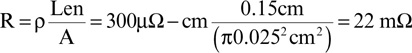
4.13 A 5-mil wide trace in ½-ounce copper is 10 inches long. What is its total DC resistance?
The sheet resistance of ½-oz. copper foil is 1 mOhm per square. To calculate the resistance of the trace, you need to know how many squares are along its length, as each square is 1 mOhm of resistance.
The number of squares is 10 inches/0.005 inches = 2,000 squares. The series resistance is 2,000 squares × 1 mOhm/square or 2 Ohm. This narrow trace, spanning 10 inches, has a resistance of 2 Ohms. This many not be much in a digital circuit, but if it is in a power path, it can be a lot.
4.14 Why does every square cut out of the same sheet of conductor have the same edge to edge resistance?
If you have a piece of sheet cut in the same of a square and measure the edge to opposite edge resistance, you would see that if the distance between the edges doubled, the resistance would double. But if you doubled the width, the resistance would be cut in half.
If you do both, double the length and double the width, you still have a square and the resistance stays the same.
You can see this when looking at the resistance based on the geometry
If in your interconnect, you keep the ratio of the length of the interconnect and the width of the interconnect the same, the resistance does not change. And if the ratio is 1, so you have a square shape, the resistance from edge to edge of the square is a constant that just depends on the bulk resistivity and the foil thickness, which you call the sheet resistance.
4.15 When you calculate the edge-to-edge resistance of a square of metal, what is the fundamental assumption you are making about the current distribution in the square?
When you calculate the edge to edge resistance, you are assuming that the current flows uniformly down the length of the square. You launch the current into the edge and take it out of the other end so that there is the same current density everywhere in the square of conductor. If you make contact with a point on the edge, the resistance you measure would be higher.
4.16 What is the resistance per length of a signal line 5 mils wide in ½-ounce copper?
In half-ounce copper, the sheet resistance is 1 mOhm/sq. A line that is 5 mils wide would have a resistance per length of 1 mOhm/sq/(0.005 inch) = 0.2 Ohms per inch.
4.17 Surface traces are often plated up to 2-ounce copper thickness. What is the resistance per length of a 5-mil wide trace on the surface compared to on a stripline layer where it is ½-ounce thick?
When the thickness of the conductor increases, there is more cross-sectional area for the current to travel and the sheet resistance and the resistance per length of the conductor decreases.
In going from ½ oz. copper in a stripline layer to 2 oz. copper on the surface, the thickness has increased by 4×. This means the resistance has decreased by ¼. The resistance per length of a 5-mil wide trace in ½ oz. copper is 0.2 Ohms/inch. This same trace fabricated on the surface has a resistance of ¼ this, or 0.05 Ohms/inch.
4.18 To measure the sheet resistance of ½-ounce copper using a 4-point probe to 1%, you are resolving a resistance of 1 µOhm. If you use a current of 100 mA, what is the voltage you have to resolve to see such a small resistance?
In order to measure a resistance of 1 µOhm, with a forcing current 0.1 A, the voltage that you would have to measure is V = I × R = 0.1 A × 1 µOhm = 0.1 µV = 100 nV. This is a very tiny voltage.
This means that for routine sheet resistance measurements, an instrument would need to be able to routinely measure 100 nV signal. It is no wonder that these measurements are rather difficult.
4.19 Which has higher resistance: a copper wire 10 mil in diameter and 100 inches long, or a copper wire 20 mils in diameter but only 50 inches long? What if the second wire were made of tungsten?
You could answer this question by calculating the resistance of each wire and looking to see which is larger. Alternatively, you can use scaling to estimate the different resistance.
The first copper wire is 10 mil in diameter and 100 inches long. The second wire is 20 mils in diameter and 50 inches long. This one is obvious. The smaller cross-section wire will have a higher resistance per length. And, it’s longer. Clearly the first wire will have higher resistance.
Suppose you made the second wire out of tungsten. Which wire would be higher resistance?
Now you can apply scaling. The resistance of the wire is basically
The length of the second wire is ½ that of the first wire. The cross-sectional area is 4× that of the first wire. These two factors alone would make the resistance of the second wire ½ /4 = 1/8th that of the first wire. The resistivity of copper is 1.68 × 10⁻⁸ Ohm-m. The resistivity of tungsten is 5.6 × 10⁻⁸ Ohm-m. This is a factor of 3.3 × higher for the second wire.
This makes the second tungsten wire, a factor of 3.3/8 = 0.42, as large as the first wire. Even with the higher resistivity, the shorter length and larger diameter overcompensates for the higher resistivity.
4.20 What is a good rule of thumb for the resistance per length of a wirebond?
A wire bond, usually made from 1-mil diameter aluminum or gold wire, has a resistance of about 1 Ohm/inch. If the wire bond is 0.1 inches long, its resistance will be 0.1 Ohms.
4.21 Estimate the resistance of a solder ball used in a chip attach application in the shape of a cylinder, 0.15 mm in diameter and 0.15 mm long with a bulk resistivity of 15 µOhm-cm. How does this compare to a wire bond?
The resistance of a uniform cross-section interconnect is
The resistance per length, for this case of a 0.15-mm diameter cylinder, is then just

The resistance per length of a wire bond is about 20 × the resistance per length of a solder ball. This is mostly due to the larger diameter of the solder ball. If the ball is 0.15 mm long, the resistance of the solder ball will be 0.021 Ohm/cm × 0.015 cm = 0.0003 Ohms. This resistance is pretty insignificant compared to other sources of resistance in the path.
4.22 The bulk resistivity of copper is 1.6 µOhms-cm. What is the resistance between opposite faces of a cube of copper 1 cm on a side? What if it is 10 cm on a side?
The resistance from one face of a cube, 1 cm on a side, to the other, is
If the side of a cube is 10 cm, larger by 10×, the resistance will be lower by 10×, to 0.16 µOhm.
4.23 Generally, a resistance less than 1 Ohms is not significant in the signal path. If the line width of ½-ounce copper is 5 mils, how long could a trace be before its DC resistance is > 1 Ohms?
When the line width for ½ oz. copper is 5 mils, the resistance per length is 1 mOhm/sq /0.005 inches = 0.2 Ohms/inch. This means a length of Len × 0.2 Ohms/inch > 1 Ohms, means a length of > 5 inches has a DC resistance > 1 Ohms. This does not mean the interconnect will not work if it is longer than 5 inches. It just means you should pay attention to see if the 1 Ohm DC series resistance is significant.
4.24 The drilled diameter of a via is typically 10 mils. After plating it is coated with a layer of copper equivalent to about ½-ounce copper. If the via is 64 mils long, what is the resistance of the copper cylinder inside the via?
You can approach this problem in two ways. You can just take the cross-sectional area and length and calculate the end-to-end series resistance. Alternatively, you can do a simpler analysis.
If you slit the via from top to bottom and unwrap the via to flatten it out, the width of the trace would be the circumference, or 3.14 × 10 mils = 32 mils. The length of the via is 64 mils. This means it is about 2 squares long. If the sheet resistance is 1 mOhm/sq and it is 2 squares long, the series resistance of the via will be about 2 mOhms.
4.25 Sometimes, it is recommended to fill the via with silver filled epoxy, with a bulk resistivity of 300 µOhm-cm. What is the resistance of the fillet of silver filled epoxy inside a through via? How does this compare with the copper resistance? What might be an advantage of a filled via?
You can estimate the resistance of the fillet of silver filled epoxy. The resistance will be
You see that the resistance of the silver filled epoxy is more than 10× larger than the copper in the wall of the via. Filling the via with silver filled epoxy will not reduce the series resistance of the via very much.
The value of using silver filled epoxy is so that the top surface is flat and solderable.
4.26 Engineering change wires on the surface of a board sometimes use 24 AWG wire. If the wire is 4 inches long, what is the resistance of the wire?
The resistance of 24 AWG wire is about 0.08 Ohms/m or 2 mOhms/inch. With a wire that is 4 inches long, the resistance of the engineering change wire would be 2 mOhms/inch × 4 inches = 8 mOhms. This is generally a small value and not a significant contribution to the electrical properties of the engineering change wire.
Chapter 5
5.1 What is capacitance?
Capacitance is usually defined as the ratio of the charge separated between two conductors to the voltage between them. While this is correct, it doesn’t say much about what really is capacitance.
The principle behind capacitance is that when you separate charges on two adjacent conductors, there is a voltage difference between them. The capacitance between the plates is really a measure of how efficient the conductors are at storing charge, at the price of voltage.
The more charge you can store for a small amount of voltage difference, the more capacitance the conductors have. If you have conductors that are not very efficient, they can’t store much charge before the voltage goes way up.
The capacitance of two conductors is not related to how much charge is on the conductor, nor what the voltage is. It is about the efficiency of storing the charge at the cost of voltage.
5.2 Give one example where capacitance is an important performance metric.
The input gate capacitance of a receiver is concentrated in a very small region at the pad on the die and directly below it. When a signal is received, it is coming from some impedance—either the drivers output impedance, or the transmission line’s characteristic impedance.
When the signal reaches the gate capacitance, the voltage is increased as current flows in. The time it takes for the input gate capacitor to charge up is a measure of the received signal rise time.
The larger the input gate’s capacitance, the longer it takes to charge and the longer the rise time at the receiver. When this rise time becomes a significant fraction of the unit interval, timing problems result.
5.3 What are two different interpretations of what the capacitance between two conductors measures.
Interpretation 1: Capacitance is the ratio of the charge stored to the voltage across the two conductors. It is a DC effect.
Interpretation 2: Capacitance is a measure of how much current will flow through two conductors separated by an insulating dielectric driven by a dV/dt. The larger the dV/dt, the larger the current through the capacitor. For a fixed dV/dt, the larger the capacitance, the more the current through the conductors.
Interpretation 3: Capacitance is the efficiency by which two conductors store a charge difference, at the cost of the voltage between them. The more efficient they are at storing charge without increasing the voltage much, the more their capacitance.
5.4 A small piece of metal might have a capacitance of 1 pF to the nearest metal, inches away. There is no DC connection between these pieces of metal. At 1 GHz, what is the impedance between these conductors?
The impedance of a capacitor at some frequency, f, is
It is rather remarkable that a piece of metal just sitting in air, with no connection to another piece, can have as low as 160 Ohm impedance between it and an adjacent conductor, at 1 GHz. This is a very low impedance between two conductors that are not touching.
5.5 How does conduction current flow through the insulating dielectric of a capacitor?
Conduction current does NOT flow through the insulating dielectric of a capacitor. It’s an insulating dielectric. There is a very small amount of leakage current that flows through a capacitor due to ion motion, or leakage current, but this tiny amount plays no role in signal quality—just in very low-level currents less than 1 nA.
5.6 What is the origin of displacement current, and where will it flow?
Displacement current is the term Maxwell introduced to account for continuity of current through an insulating dielectric. He said displacement current flowed along electric field lines whenever the E field changed. The amount of displacement current was precisely the dE/dt.
Between any two conductors with a voltage difference, there will be an electric field. If the voltage changes, the electric field changes and the displacement current flows along the field lines between the conductors.
In his world view, Maxwell thought even empty space was filled with the ether. Between the two plates of a capacitors, filled with vacuum, was really ether. And to Maxwell, the ether was polarizable.
When the electric field between the plates changes, the E field polarized the ether particles and pulled the + and − charges of the ether particles farther apart, displacing them. This displacement of charges in ether particles, when the E field changed, he coined as displacement current.
It referred to the motion of bound charges, as distinct from free charges that could move in a conductor, as conduction currents.
To this day, we still call the current that flows when E fields change displacement current, but attribute it to a property of space-time, rather than to the polarization of ether particles.
5.7 If you wanted to engineer a higher capacitance between the power and ground planes in a board, what three design features would you change?
To increase the capacitance between two conductors, you bring the conductors closer together and increase the overlap width and overlap length of the two planes.
5.8 What primary property about the chemistry of a dielectric most strongly influences its dielectric constant?
The dielectric constant of a material is a measure of how much it increases the capacitance of two conductors when inserted between them. The way it does this is to shield a little of the electric field between the two conductors by polarizing the bound charges inside the material.
A high dielectric constant material usually is a very polarizable material. This means it has a lot of bound charges that can be separated. The most common process is to have large dipoles in the material that can rotate in the electric field.
High Dk materials usually have large dipoles that are mobile and can rotate and align in an electric field. Water is a perfect material with a large dipole that can rotate in an electric field. This is why water has a Dk of 80.
Polymer materials with a high Dk have dipole groups, either tied off the backbone chin, or integrated in the backbone chain that can rotate and align in an external electric field.
The epoxy polymers incorporate a C-O-C group in the polymer backbone. This group has a large dipole and can rotate in an external E field.
Materials with a low Dk value do not have many dipoles that can rotate. Teflon, or PTFE, polytetrafluoroethylene, is just a carbon backbone with fluorine atoms along the chain. There is not dipole that can rotate and very little structure that can be polarized.
5.9 What happens to the capacitance between two conductors when the voltage between them increases?
Trick question. Nothing. Capacitance is the ratio of the charge stored to the voltage difference between two conductors. This ratio is independent of the amount of charge stored, or the voltage between the conductors.
When the voltage increases, the capacitance, which is just about the geometry, stays the same. It’s the charge separation between the conductors that changes.
5.10 In a coax geometry, what happens to the capacitance if the outer radius is increased?
If two conductors are moved farther apart, their capacitance decreases. In a coax, if the outer conductor radius is increased and the outer conductor moves farther away from the inner conductor, the capacitance of the coax decreases.
5.11 What happens to the capacitance per length in a microstrip if the signal path is moved away from the return path?
When the signal and return paths of any conductor topology are pulled farther apart, the capacitance decreases.
5.12 Is there any geometry in which capacitance increases when the conductors are moved farther apart?
No.
5.13 Why does the effective dielectric constant increase as the thickness of the dielectric coating increases in microstrip?
As the thickness of the dielectric over a microstrip trace increases, the capacitance of the microstrip will increase. Where some fringe fields were in air before the dielectric coating, after the coating, these fringe fields see a higher Dk. This means the overall capacitance increases.
The geometry hasn’t changed, just the distribution of dielectric material. You describe the increase in capacitance as an increase in effective dielectric constant.
5.14 What is the lowest dielectric constant of a solid, homogenous material? What material is that?
The lowest dielectric constant of a solid homogenous material is 2. One example of such a material is Teflon. It has no net dipoles that can move. It is only the electrons within the molecules that can displace and polarize in an electric field.
When a material has no dipoles and it’s only the electrons in the molecules that can polarize in an external electric field, its dielectric constant will be the lowest possible, with a value of about 2.0.
5.15 What could you do to a material to dramatically reduce its dielectric constant?
One trick that is often used in interconnects to reduce the Dk of a dielectric is to foam it. By foaming the material, you add air to it and decrease its density. You can take Teflon or Polyethylene, foam it and reduce its dielectric constant to nearly 1, close to air. This is as low as it is possible to get. Foamed Teflon is often used in high-performance cables.
5.16 What happens to the capacitance per length of a microstrip if solder mask is added to the top surface?
When solder mask is added to the top of a microstrip, some fringe field lines that were in air now see a higher DK material. This increases the capacitance between the signal and return path of the microstrip.
5.17 What happens to the capacitance per length of a microstrip if the conductor thickness increases?
If the conductor thickness increases, there will be a few more fringe field lines from the edge of the thicker signal trace to the return plane. This increases the capacitance between the signal and return path a little bit.
5.18 What happens to the capacitance per length of a stripline if the line width increases?
If the line width increases, the area of overlap between the signal and return paths increases, and the capacitance per length increases.
5.19 What happens to the capacitance per length of a stripline if the trace thickness increases?
If the trace thickness increases, and the separation between the two planes of the stripline stays the same, then the distance between the top surface of the signal line to either plane will decrease. The spacing between the signal line and return will be closer, and this will increase the capacitance between the two conductors.
5.20 For the same line width and dielectric thickness per layer, which will have more capacitance per length: a microstrip or a stripline?
A microstrip signal line will have a capacitance to just one plane, while a stripline trace will have a similar value capacitance to each of two planes in parallel. The stripline trace would have a higher capacitance per length than the microstrip trace, if the line widths were the same and the dielectric thickness per layer were the same.
5.21 What is theoretically the lowest dielectric constant any material could have?
No material can have a dielectric constant lower than 1, which is the dielectric constant of air. Some materials made of a foam and used in cable applications can approach this value. If the material is solid and homogenous, the lowest Dk it can have is about 2. This is limited by the polarizability of electrons in the molecules that make up the material. As dipoles that can rotate are added to the material, the Dk will increase.
5.22 Why is the capacitance per length constant in a uniform cross-section interconnect?
The capacitance between two conductors depends on the spacing between the two conductors and their area of overlap. In a uniform transmission line, the spacing between the signal and return paths are constant down the length, and the width of the conductor is constant. This means the capacitance for a fixed length will be constant.
5.23 On die, the dielectric thickness between the power and ground rails can be as thin as 0.1 micron. If the SIO2 dielectric constant is also 4, how does the on-die capacitance per square inch compare to the on-board capacitance per square inch if the power and ground plane separation is 10 mils?
The capacitance of two plates with the same area and Dk value will scale inversely with the dielectric thickness. A 10-mil thick separation is really 250 microns. This is 2500 times larger than the dielectric thickness on die. This means the on-die capacitance per area between the power and ground rails will be 2500 times higher than in a typical circuit board.
5.24 What is the capacitance between the faces of a penny if they are separated with air?
A penny has faces that are about 0.5 square inches in area and are separated by about 0.1 inch. The capacitance of two conductors can be calculated from
The capacitance between the two faces of a penny if they were isolated planes, would be about 1 pF. Of course, in a penny, the two faces are not separated by a dielectric of air—they are connected together with the rest of the copper, so they have no capacitance. But if two plates are in the shape of a penny, separated by the same distance, they would have a capacitance of about 1 pF.
Thinking about the size and shape of a penny is a good calibration for how much capacitance there is in 1 pF.
5.25 What is the minimum capacitance between a sphere 2 cm in diameter suspended a meter above the floor? How does this capacitance change as the sphere is raised higher above the floor?
The capacitance of a sphere when other conductors are 100 diameters away is just
If you hold the 2-cm diameter sphere 1 m over the surface of the floor, its capacitance will be slightly higher than this. But as you move it farther and farther away, it will roughly approach this value. You see that the capacitance, in pF, is about equivalent to the diameter of the sphere. This is a rough calibration of the capacitance in a piece of metal just suspended away from the floor. You can never get away from stray capacitances between any piece of metal and some grounded surface somewhere. Everything couples.
5.26 What is the capacitance between the power and ground planes in a circuit board if the planes are 10 inches on a side, 10 mils separation, and filled with FR4?
To calculate the capacitance between two planes, you can always start with the parallel plate approximation. It takes less than 1 minute to set it up, put in the values, and calculate the capacitance.
In addition, you can get to an estimate for the special case of two planes with an FR4 dielectric between them using the simple approximation that

With a dielectric thickness of 10 mils, the capacitance per unit area is just 0.1 nF/in2. If the area of the plates is 10 in × 10 in = 100 in2, the capacitance between the planes is 0.1 nF/in2 × 100 in2 = 10 nF.
5.27 Derive the capacitance per length of the rod over a plane from the capacitance per length of the twin rod geometry, in air.
The capacitance between two parallel rods, with radius r and center to center separation of s, in air, is
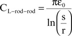
You should never use a relationship without first applying rule #9. Is it reasonable? Does it match your expectations? As you pull the rods farther apart, the capacitance should decrease. When s increases, the denominator increases, and the capacitance per length will decrease. This matches what you expect. It doesn’t mean this is a good approximation, just that it is consistent with one simple test.
If you place a conducting plane in the middle between the two rods, the electric field distribution will not change. The capacitance between the two rods will not change. But, you can describe it as the series combination of the capacitance between one rod and the plane in series with the capacitance of the second rod and the plane.
These two capacitances in series add up to the capacitance of the two rods. This means the capacitance between the rod and plane in this configuration is 2 × the capacitance between the two rods:
CL–rod–plane = 2 × CL–rod–rod
If you replace the separation, s with 2 × h, the capacitance of the plane to rod can be calculated as
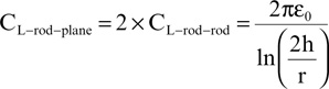
This is the capacitance between a rod and plane.
Chapter 6
6.1 What is inductance?
Inductance is the efficiency with which a conductor can create rings of magnetic field lines at the cost of the current through it. If a conductor can generate a lot of rings of magnetic field lines with a little current, it has a high inductance. If it generates only a few rings of magnetic field lines per amp of current through it, it has a low inductance.
6.2 What are the units used to count magnetic field lines?
You count rings of magnetic field lines in units of Webers. A Weber of rings of field lines is some number of rings.
6.3 List three properties of magnetic field lines around currents.
The magnetic field lines around a current in a wire are in the shape of complete circles or closed rings.
These rings have a direction of circulation. The direction is based on the right-hand rule. Point the thumb of your right hand in the direction of the positive current and your fingers curl in the direction of circulation of the rings of magnetic field lines.
If you count the number of rings of field lines around a wire, you find this number, measured in Webers of field lines, is directly proportional to the current in the wire. Double the current, and the number of Webers of field line rings will also double.
The density of rings of field lines will drop off as you move away from the wire. The rings get farther apart and you see fewer and fewer rings, the farther you move from the conductor.
6.4 How many field line rings are around a conductor when there is no current through it?
This is a trick question. With no current in the conductor, there will be no rings of magnetic field lines around the conductor.
6.5 If the current in a wire increases, what happens to the number of rings of magnetic field lines?
If the current in a wire doubles, the number of rings of magnetic field lines will exactly double as well. The number of Webers of rings of field lines around a conductor is directly proportional to the current in the wire.
6.6 If the current in a wire increases, what happens to the inductance of the wire?
Trick question. If the current in a wire doubles, the number of Webers of rings of magnetic field lines will double, but the ratio of the Webers of field lines to the current stays the same. Inductance is independent of the current in the wire. A conductor has an inductance even with no current in the wire. It is a measure of the efficiency of generating rings of magnetic field lines, not of the number of field lines present.
6.7 What is the difference between self-inductance and mutual inductance?
Self-inductance is a measure of the rings of magnetic field lines around a conductor per amp of current through that conductor. It is a measure of the efficiency of a conductor at creating rings of magnetic field lines around itself.
Mutual inductance is a measure of the number of rings of magnetic field lines around another conductor, per amp of current in the first conductor. It is a measure of the efficiency of creating rings of field lines around another conductor at the cost of current through the first conductor.
6.8 What happens to the mutual inductance between two conductors when the spacing between then increases? Why?
When you pull two conductors apart, you decrease the mutual inductance between them. If one conductor has current in it, there will be rings of magnetic field lines around it. The density of the rings will drop off the farther away you go from the conductor.
When there is an adjacent conductor present, some of the rings of field lines from the first conductor will also be around the second conductor. These are the mutual field lines. The farther away the second conductor, the fewer rings of field lines will be present to go around this second conductor.
The farther apart the two conductors, the lower the mutual inductance.
6.9 What two geometrical features influence the self-inductance of a conductor?
The two most important design terms that influence the self-inductance of a conductor are its length and the current distribution inside the conductor.
The longer the length, the more distance you have to count rings of field lines for the same current in the conductor and the higher the self-inductance.
The tighter you constrict the current distribution in the conductor—by using a narrower conductor, for example—the more rings of magnetic field lines you can count around the conductor, and the higher the self-inductance.
6.10 Why does self-inductance increase when the length of the conductor increases?
The self-inductance is a measure of how many Webers of field lines you count around the conductor per amp of current through the conductor. The longer the conductor, the more length you have to count field lines around.
6.11 What influences the induced voltage on a conductor?
The inducted voltage between two points on a conductor depends on how fast the total number of rings of field lines change around the conductor. If the number of Webers of field lines around the conductor between the two points is the same, there will be no voltage induced.
But, if the number of Webers of field lines changes, for whatever reason, there will be an induced voltage.
6.12 What is the difference between partial and loop inductance?
Inductance, in general, is about the efficiency of creating rings of field lines around a conductor at the cost of the current through it. When you set up a real conductor and send current through it, you can only do this with current flowing in a complete loop.
The question you have to address is what part of the loop are you counting the rings of field lines around, and are you counting the total number of rings of field lines around each section of the loop as you walk down the length of the loop?
After all, if you are at one piece of the loop, counting rings of field lines, you will see some of the rings as coming from the current in that section of the loop, but some of the field lines will also be coming from the section of the loop that has the return current flowing in the exact opposite direction. Its rings of field lines around your section of the loop will be circulating in the opposite direction. These two different sets of rings of field lines around the section of the loop you are sitting on will subtract.
When you walk along the loop from one end to the other, counting the entire number of rings of field lines, taking into account the direction of circulation of each one, the inductance you get is the loop inductance of the loop. This is unambiguous. There is only one value for the loop inductance of the loop.
But, when you only want to consider a part of the loop, and count only those specific field lines coming from the currents in that part of the loop, ignoring the other rings of field lines around your part of the loop from other currents, you call this inductance the partial inductance, and specifically, the partial self-inductance.
6.13 Why does the mutual inductance subtract from the self-inductance to give the total inductance when the other conductor is the return path?
A ring of magnetic field lines has a direction of circulation. The total number of rings of field lines around a section of a conductor depends on how many circulate one way and the other. They subtract from each other, and a ring in one direction cancels a ring circulating in the other direction.
When counting the total number of rings around a conductor, all the rings from its own current, the self-field lines, will be in the same direction and add together. But, the mutual field lines from the return current, since the return current is flowing in the opposite direction, will circulate in the opposite direction around the conductor.
The mutual-field lines, being in the opposite direction around the current than the self-field lines, will subtract. This means the presence of the adjacent return current will result in fewer net rings of magnetic field lines around the first conductor, per amp of current in the conductor.
6.14 In what cases should the mutual inductance add to the self-inductance to give the total inductance?
Whenever the two currents flow in the same direction, the mutual field lines between them will add to their self-field lines to create a larger total number of field lines.
Not all adjacent currents are return currents. If there is another adjacent conductor with current from a different source flowing in the same direction as the first current, its self-field line rings will circulate in the same direction as the first current.
Those mutual field lines from this adjacent current, in the same direction as the first current, around the first current, will also circulate in the same direction as the self-field lines of the first current.
The total number of rings of field lines around the first current will be the sum of its self-field lines and the mutual-field lines from the adjacent current.
6.15 What three design features will decrease the loop inductance of a current loop?
The total number of rings of magnetic field around a loop depends on the length of the loop, the width of the conductor through which current is flowing, and the proximity of the return half of the loop to the first half of the loop.
The longer the loop, the larger the loop inductance. The smaller diameter the wire, the larger the loop inductance. The farther away the return half of the loop is from the first half of the loop, the larger the loop inductance.
6.16 When estimating the magnitude of ground bounce, what type of inductance should be calculated?
It’s the total inductance of the return path that contributes to ground bounce. After all, ground bounce is the voltage from one end to the other in the return path, due to the rate of change of the total number of rings of field lines around the return conductor.
6.17 If you want to reduce the ground bounce in a leaded package, which leads should be selected as the return leads?
There are only three knobs that affect the total inductance of the return path: the length of the return path, the width of the return path, and the proximity of the return path to the signal paths.
The length is the term that has the largest impact on the total inductance. The return pins in a package should be selected as the shortest leads. This is usually the case for the central leads in square package.
6.18 If you want to reduce the loop inductance in the power and ground paths in a connector, what are two important design features when selecting the power and ground pins?
Use pins that are short, and select the power pins adjacent to the ground pins.
6.19 There are 24 Webers of field line rings around a conductor with 2 A of current. What happens to the number of field lines when the current increases to 6 A?
The number of Webers of field lines around a conductor is directly proportional to the current through the conductor. If the current increases by 6 A/2 A = 3×, the number of Webers of field lines will increase by the same amount. It will change from 24 Webers to 24 × 3 = 72 Webers.
6.20 A conductor has 0.1 A of current and generates 1 microWeber of field lines. What is the inductance of the conductor?
The definition of inductance is that it is the ratio of the number of rings of field lines per amp of current. If there are 10–6 Webers of field lines for 0.1 A, the inductance is 10–6/0.1 = 10–7 H, or 100 nH of inductance.
6.21 A current in a conductor generates 100 microWebers of rings of field lines. The current turns off in 1 nsec. What is the voltage induced across the ends of the conductor?
The induced voltage across a wire is dN/dt. If the number of Webers changes linearly from 100 µW to zero in 1 nsec, the induced voltage during this period of time is V = 100 µW/1nsec = 100 µW/0.001 µsec = 105 V, a huge number! This is an indication that you can sometimes generate large voltages when currents turn off quickly.
This happens in relays. When the relay has current flowing through it and it opens, the current turns off very quickly and you can generate large voltages that can arc across the gap in the open relay. This is the dominant source of degradation in relays. To avoid this problem, either engineer the relay to open when there is little current flowing through it, or add a capacitor or diode across the gap to provide an alternative current path to reduce the dI/dt.
6.22 The return lead in a package has 5 nH of total inductance. When the 20 mA of current through the lead turns off in 1 nsec, what is the voltage noise induced across the lead?
The voltage across an inductor is V = LdI/dt. In this case, the L is 5 nH, the dI = 20 mA, and the dt = 1 nsec. The voltage is easily calculated as V = 5 nH × 20 mA/1nsec = 100 mV.
The most important thing to watch out for are the units. In this case, the nano in nH cancels out with the nano in the nsec to turn off time. This means the units that are left are mV.
6.23 What if four signals use the lead in Question 6.22 as their return path? What is the total ground bounce noise generated?
If the four signals all have the same 20 mA of signal current and are turning off in the same 1 nsec, and their returns all flow through the same total inductance, the dI will be 4× the case of just one signal switching.
This means the ground bounce noise will be 4× the previous case, or 400 mV of ground bounce noise.
6.24 What is the skin depth of copper at 1 GHz?
As a good rule of thumb to remember, the skin depth of copper at 1 GHz is about 2 microns.
6.25 If current flows in both the top and bottom surfaces of a signal trace on a circuit board, how much does the resistance increase at 1 GHz compared to DC?
At DC, if the conductor is composed of 1 oz. copper, such as typically found on surface traces, the sheet resistance is 0.5 mOhms/square. This is when current flows through the 34 microns of conductor thickness uniformly.
If a trace, patterned from this layer, is part of a microstrip, the current distribution will have about equal currents flowing in the top surface as in the bottom surface, each to a thickness of the skin depth. At 1 GHz, this is a thickness of 2 microns in the top and bottom. The total cross section through which current flows in the microstrip at 1 GHz is 4 microns. This is compared to the cross section for current to flow at DC of about 34 microns.
The resistance per length of the conductor at 1 GHz compared to DC will scale with the ratio of the cross-section thicknesses, as all other terms are the same. The smaller the thickness, the higher the resistance.
The 1 GHz resistance will be 34/4 = 8.5 × higher than the DC resistance in 1 oz. copper.
If the copper trace thickness were ½ oz. copper, the geometrical thickness would be 17 microns and the 1 GHz resistance would be 17/4 = 4.2 × higher than the DC resistance.
6.26 Based on the simulation results in Figure 6-26, what is the percentage of decrease in inductance from DC to 1 GHz?
The loop inductance per inch in a microstrip at DC is about 10 nH/inch. At 1 GHz, it is about 8 nH/inch for this specific characteristic impedance. This is a drop in the DC inductance of 2 nH/10 nH = 20%.
Above about 100 MHz, all the current has redistributed as much as it can, and the loop inductance is the same at 100 MHz as at 1 GHz or higher.
6.27 When the spacing between two loops doubles, does the loop mutual inductance increase or decrease?
Since you are pulling the two loops farther apart, the loop mutual inductance between them has to decrease. There will be fewer mutual field lines from one loop around the other when you pull them farther apart.
6.28 What is the loop inductance of a loop composed of 10-mil diameter wire, in a circular loop 2 inches in diameter?
The loop inductance of a circular loop is approximately

The radius of the loop is 1 inch.
6.29 What is the loop inductance per length of two rods 100 mils in diameter, and spaced by 1 inch? What is the total inductance per inch of each leg?
The loop inductance per inch of the pair of rods is roughly

In this case, the radius is 50 mils or 0.05 inches. You have to be careful of the units. The s and r terms should have the same units.
This is the loop inductance of the pair of rods, assuming current goes down one and back up the other.
You can separate this into a total inductance of each leg. The sum of the total inductances of each leg in series makes up the loop inductance, so the total inductance of each leg would be about 15 nH/inch.
6.30 A typical dielectric thickness between the power and ground planes in a 4 layer board is 40 mils. What is the sheet inductance of the power and ground planes? How does 1 square of sheet inductance compare to the typically 2 nH of mounting inductance of a decoupling capacitor?
The sheet inductance in two planes is about 32 pH/mil × h[mils]. When the spacing between the planes is 40 mils, the sheet inductance is 32 × 40 = 1.3 nH. This is the inductance per square in the planes.
This is smaller than, but of the same order, as the mounting inductance of a capacitor, if it were 2 nH. This means that the spreading inductance in the cavity from the capacitor to the package would be significant. Doing what you can to reduce the spacing between the capacitor and the package would reduce the equivalent inductance of the capacitor. In this environment, the cavity is not transparent, and positon would matter.
If you reduce the dielectric thickness between the planes to 3 mils, the sheet inductance would be 0.1 nH, which is small compared to the mounting inductance of the capacitor, and the cavity would be transparent. Location of the decoupling capacitor would not matter.
Chapter 7
7.1 What is a real transmission line?
A real transmission line is composed of any two conductors with some extended length. One conductor you label as the signal path and the other conductor as the return path.
7.2 How is an ideal transmission line model different from an ideal R, L, or C model?
At low frequency, the ideal transmission line input impedance matches the impedance of a simple L or C element depending on if the far end is open or shorted. But, at frequencies beyond some frequency, the behaviors of the L or C model drastically departs from the ideal transmission line.
This means the L or C elements are good approximations to an ideal transmission line model at low frequency. They are terrible approximations to an ideal transmission line at higher frequency. An ideal transmission line model is a brand-new circuit element with properties that are completely different from a single L or C element, which becomes apparent at very high frequency.
7.3 What is ground? Why is it a confusing word for signal-integrity applications?
The term ground should only be used to refer to the single reference point in a circuit from which all other voltages are referenced. The ground point should not carry any current.
On a plane with current flowing, not all points on the plane labeled as ground are the same voltage. This makes it difficult to use a ground plane as a reference enplane.
The term ground is often misused in the industry and confused with return path. The return path is the conductor that carries the return current. It can be at any DC voltage, and often has a different voltage across it form one region to another.
7.4 What is the difference between chassis and earth ground?
Earth ground, often referred to as safety ground, is literally a connection to the ground. There is a low-resistance path between all points labeled as earth ground to a copper pipe sticking into the ground somewhere nearby. This pipe defines a common reference point tied to the Earth from which other points can be references. As long as all points connect to the same earth ground, they will be at the same voltage and there is less chance of someone getting a shock.
Chassis ground is the connection to the external metal housing of an instrument or device. In the case of a plastic enclosure, there is no chassis ground. For safety reasons, the UL requires that chassis ground be connected to earth ground. This reduces the risk of a user getting a shock due to widely different chassis ground voltages.
7.5 What is the difference between the voltage on a line and the signal on a line?
The voltage on a transmission line is what would be measured by a scope if the probes were touching between the signal and an adjacent point on the return path. This is a scalar voltage in the sense there is no measure of the propagating nature of this voltage. It is just the total voltage between the signal and return path.
The signal is the voltage that is propagating down the line. It has a direction associated with it. When the voltage of a signal is measured, the magnitude can be the same as the magnitude of the signal, but there is no information measured about the direction of propagation of the signal.
The real difference arises when there are multiple signals propagating on the transmission line. Two signals may be propagating in opposite directions on the transmission line. When measured at one point, the voltage measured is the sum of the two voltages. It could be less than, greater than, or the same as the two signal voltages, depending on their specific properties.
7.6 What is a uniform transmission line and why is this the preferred interconnect design?
A uniform transmission line means the cross section of the transmission line is the same up and down the length of the line. This means the instantaneous impedance of the line is the same. Engineering the instantaneous impedance the signal sees as the same up and down the line means the signal will propagate with no reflections and no distortions, improving the signal quality.
If the transmission line is not uniform, there will be impedance changes that will cause reflections and signal distortions.
7.7 How fast do electrons travel in a wire?
Surprisingly, even with as much as 1 A of current in a narrow wire, the speed of the electrons is really small, on the order of 1 cm/sec. This means that it is not the motion of the electrons which is the signal, but the propagating of the changing electric and magnetic fields.
It is like the case of a tube filled with marbles. If you push one marble in one end, another will push out the far end in the time it takes for the pressure wave to flow down between the marbles. The speed of the marble moving down the tube is slow, but the speed of the impact of the motion of the marble is very fast.
7.8 What is the difference between conduction current, polarization current, and displacement current?
Conduction current is the flow of free charges in a conductor. There can be DC current flow with a DC voltage applied.
Polarization current is the current that flows in an insulator when the polarization of bound charges changes. This is literally a motion of charges, but they are restricted to staying attached to the molecules of the dielectric. They will only flow when the polarization of the material changes, which is when the extern E field changes. These currents are transient and are proportional to dE/dt.
Displacement current is the current that flows in the air when the electric field changes. Maxwell called the displacement current the current that flows due to the changing polarization of the charges in the ether. Today, you do not have to invoke the ether, but describe displacement current, as a current that flows when the electric field changes, as a feature of electric fields built into the fabric of space time.
7.9 What is a good rule of thumb for the speed of a signal on an interconnect?
In air, the speed of a signal, or the speed of light, is 12 inches/nsec. When propagating through a dielectric with dielectric constant Dk, the speed of the changing electric field, which is light, slows down with the square root of the Dk.
The typical Dk for most interconnect materials is about 4. This means the speed of a signal on a typical laminate interconnect substrate is about 12/sqrt(4) = 6 inches/nsec.
This is a good rule of thumb for the speed of a signal on an interconnect, about 6 inches/nsec.
7.10 What is a good rule of thumb for the aspect ratio of a 50-Ohm microstrip?
With an FR4 substrate, the ratio of the line width to dielectric thickness of a 50-Ohm transmission line is 2/1.
7.11 What is a good rule of thumb for the aspect ratio of a 50-Ohm stripline?
In a stripline geometry, and FR4 substrate, the aspect ratio of the line width and dielectric spacing between the planes is ½. Since there are two planes, the dielectric thickness must be larger in stripline than in microstrip.
7.12 What is the effect called when the dielectric constant and the speed of a signal are frequency dependent?
When the dielectric constant varies with frequency, or the speed of the signal varies with frequency, you call this effect dispersion. It is a frequency-dependent speed of the signal.
7.13 What are two possible reasons the characteristic impedance of a transmission line would be frequency dependent?
The characteristic impedance of a transmission line depends on the inductance per length and capacitance per length of the line. Both of these are slightly frequency dependence.
For example, the inductance per length of the line will be higher at low frequency and drop about 10% to 20% at higher frequency. This makes the characteristic impedance higher at low frequency and lower at high frequency, by the square root of 10−20%.
The capacitance per length of a transmission line will also be slightly frequency dependent due to the frequency dependence of the dielectric constant.
At low frequency, the DK is typically a little larger than at high frequency. This makes the characteristic impedance slightly lower at low frequency, increasing at high frequency.
While these two effects move the characteristic impedance in opposite directions, their different frequency dependence, and different magnitudes, means they do not cancel out. There is still some net frequency dependence of the characteristic impedance, typically on the order of less than 10% from low to high frequency.
7.14 What is the difference between the instantaneous impedance and the characteristic impedance and the input impedance of a transmission line?
Although all three of these terms are impedances, they refer to different features. The instantaneous impedance is the impedance the signal sees each step along its path as it propagates down the transmission line. This is the impedance the propagating signal responds to at each step.
The characteristic impedance only applies to a uniform transmission line and is the one value of instantaneous impedance the propagating signal will see. If the instantaneous impedance changes, there is no one value of instantaneous impedance that characterizes the transmission line.
The input impedance of the transmission line is usually a frequency-domain term, and is the impedance you see looking into the front of the transmission line at specific frequencies. The input impedance will vary a lot with frequency.
7.15 What happens to the time delay of a transmission line if the length of the line increases by 3×?
The time delay of a transmission line is directly proportional to the length of the line. If you triple the length of the line, the time delay of the line will triple as well.
7.16 What is the wiring delay of a transmission line in FR4?
We sometimes refer to the inverse of the speed of a signal as the wiring delay. It is the delay per length of the line. If the speed of the signal is 6 inches per nsec, the wiring delay is 1/(6 inch/nsec) = 170 psec/inch.
This means the delay is 170 psec per inch of travel down the transmission line.
7.17 If the line width of a transmission line increases, what happens to the instantaneous impedance?
If the line width of a transmission line increases, the capacitance per length of the line increases and the instantaneous impedance decreases. The wider the line, the lower the instantaneous impedance. If the line is uniform, the characteristic impedance would also decrease for wider lines.
7.18 If the length of a transmission line increases, what happens to the instantaneous impedance in the middle of the line?
This is a trick question. If the length of the line increases, the instantaneous impedance stays exactly the same. The time delay of the line increases, but the instantaneous impedance stays the same.
7.19 Why is the characteristic impedance of a transmission line inversely proportional to the capacitance per length?
If the capacitance per length increases, it takes more current to charge up each small step in the transmission line. If more current is required to charge up the line to the same voltage, the impedance decreases. This means the capacitance per length is inversely related to the instantaneous impedance.
7.20 What is the capacitance per length of a 50-Ohm transmission line in FR4? What happens to this capacitance per length if the impedance doubles?
All 50 Ohm lines in FR4 have the same capacitance per length of about 3.3 pF/inch. If the line width increases, but the dielectric thickness increases to keep the characteristic impedance the same, the wider line transmission line will have the same capacitance per length.
If the characteristic impedance of the line increases, the capacitance goes down. They are inversely related. If the line impedance doubles, the capacitance per length is cut in half.
7.21 What is the inductance per length of a 50-Ohm transmission line in FR4? What if the impedance doubles?
All 50 Ohm transmission lines in FR4 have an inductance per length of about 8.3 nH/inch. Of course, if one dimension changes, the other dimensions need to change to keep the 50 Ohms.
And the line impedance is directly proportional to the inductance per length. If you double the impedance of the line, you will double the inductance per length of the line.
7.22 What can you say about the capacitance per length of an RG59 cable compared to an RG58 cable?
These two coax cables use the same dielectric. They have the same central conductor radius. But, they have different characteristic impedance. An RG58 cable has a characteristic impedance of about 50 Ohms, while an RG59 cable has a characteristic impedance of 75 Ohms.
The higher impedance cable will have a lower capacitance per length. This is also seen in that the outer dimeter of an RG59 cable is larger than an RG58 cable. The outer conductor, being father away, makes the capacitance per length lower in the RG59 cable.
7.23 What do we mean when we refer to “the impedance” of a transmission line?
Just referring to “the impedance” of a line is ambiguous. It could refer to the instantaneous impedance, the characteristic impedance, the input impedance in the frequency domain, or the input impedance in the time domain. Without some specific context, you don’t know which one is of interest.
Unfortunately, you get lazy and often drop the qualifier. More often than not, when you refer to just the impedance of the line, you mean the characteristic impedance of the transmission line. Even though you may refer to the characteristic impedance, this does not mean that it is the same as the impedance the driver might see unless the rise time is very short and the line very long, and you only look for a very short period of time.
7.24 A TDR can measure the input impedance of a transmission line in a fraction of a nanosecond. What would it measure for a 50-Ohm transmission line, open at the end, that is 2 nsec long? What would it measure after 5 seconds?
The TDR sends a short rise-time step edge down the transmission line and measures the reflected signal. It is usually launched from a 50 Ohm source. If the transmission line it is connected to is 50 Ohms, there will be no reflection, so there will be no reflected signal when the signal enters the transmission line.
The step edge will travel down the transmission line, reach the end, and reflect from the open. The reflected edge will take about 4 nsec after being launched into the line to make it back to the front of the instrument.
Once it is into the instrument, nothing more reflects and no additional signal enters the transmission line.
The TDR will measure a 50 Ohm line initially, then 4 nsec later, an open. It will measure an open forever afterward. After 5 seconds, the TDR will measure an open.
7.25 A driver has a 10-Ohm output resistance. If its open circuit output voltage is 1 V, what voltage is launched into a 65-Ohm transmission line?
The driver and transmission line create a voltage divider. The transmission line looks like a 65 Ohm resistor with the 10 Ohm driver impedance in series. The voltage drop across the 65 Ohm resistor is 1 V × 65 Ohms/(10 Ohms + 65 Ohms) = 0.87 V.
7.26 What three design features could be engineered to reduce the impedance of the return path when a signal changes return path planes?
When a signal transitions its return path between two planes, the return current sees the impedance between the planes in series with the impedance of the line. To minimize the discontinuity and the noise coupled into the cavity, you want to decrease the impedance of the cavity.
The most important way is to add shorting vias. This means you have to use the same voltage for the two planes.
The second feature, which applies no matter what the voltage of the two planes may be, is to use a thin dielectric between the two planes. This dramatically reduces the impedance between the planes if they are different voltages, and makes the shorting vias more effective if they are not.
Finally, if the two planes are different voltages so shorting vias can’t be used, a DC blocking cap can be placed between the shorting vias. It will never have as low an impedance as shorting vias, but it is a compromise.
7.27 Which is a better starting model to use to describe an interconnect up to 100 MHz: an ideal transmission line, or a 2-section LC network?
An ideal transmission line is always a better model to use to describe a real interconnect than an n-section LC model. The ideal transmission line model will look like the L and C elements at low frequency, but match the properties of the real transmission line to much higher frequency than any LC model.
And the transmission line model is a much simpler model to use. All SPICE simulators understand the ideal transmission line model, and many of them have lossy transmission line models and coupled transmission line models.
7.28 An interconnect on a board is 18 inches long. What is an estimate of the time delay of this transmission line?
The speed of a signal in FR4 is about 6 inches per nsec. The delay of any transmission line is about Len[inches]/v[inch/nsec] = 18 inches/6 inches/ nsec = 3 nsec.
7.29 In a 50-Ohm microstrip, the line width is 5 mils. What is the approximate dielectric thickness?
In a 50-Ohm transmission line in FR4, the ratio of the line width to dielectric thickness is about 2 to 1. If the line width is 5 mils, the dielectric thickness should be about 2.5 mils. A common thickness laminate available is about 2.8 mils.
7.30 In a 50-Ohm stripline, the line width is 5 mils. What is the length of the transmission line?
This is a trick question. Just knowing the characteristic impedance and the line width tells you nothing about the length of the line. It could be 1 inch, or it could be 30 inches. You would need to know about the time delay of the line, or the total inductance or total capacitance. Just the line width and impedance is not enough information.
Chapter 8
8.1 What is the only thing that causes a reflection?
Reflections are only caused by the signal encountering a change in the instantaneous impedance. If there is a reflection, this means the instantaneous impedance has changed. It could be caused by a line width change, a dielectric thickness change, or some other geometry feature change.
8.2 What two features influence the magnitude of the reflection coefficient?
The reflection coefficient between two impedances is only about the ratio of the difference in impedance divided by the sum of the two impedances. These are the only two parameters that affect the reflection coefficient, the two instantaneous impedances at the interface.
8.3 What influences the sign of the reflection coefficient?
The reflection coefficient is the second impedance minus the first impedance over their sum. If the second impedance is larger than the first impedance, the sign is positive. If the second impedance is smaller than the first impedance, the sign is negative. This is the ONLY thing that influences the sign of the refection coefficient.
8.4 What two boundary conditions must be met on either side of any interface?
When you look at the interface, you need to see continuity in the voltage between the signal and return paths. There can’t be a step change in the voltage between the signal line on the left side and the right side. Otherwise, there could be an infinitely large electric field across the interface and the universe could explode.
In addition, you must see the same current circulating on the left side of the interface as on the right side of the interface. This means there is no net current circulating at the interface. If there was a net current into the interface, the interface would charge up, and if you waited long enough, the universe would explode.
You call these two conditions, boundary conditions, continuity of voltage and conservation of charge.
8.5 When viewed at the transmitter, how long does a reflection from a discontinuity last?
When a signal encounters a short discontinuity in an otherwise uniform transmission line, there will be a reflection from the front of the discontinuity and a reflection from the back of the discontinuity.
From the time of the reflection from the front interface, it will take a round-trip time down through the discontinuity, hitting the end of it, and then passing through it again for the reflection to make its way out of the discontinuity to head to the transmitter.
This means the reflected signal to the transmitter will last for a round-trip time through the discontinuity.
If the discontinuity is 1-inch long, its time delay is about 170 psec. The reflected signal will be a pulse with a width of about 170 psec × 2 = 340 psec.
8.6 What is the difference in reflection coefficient when a signal reflection from a 50-Ohm line hits a 75-Ohm transmission line or a 75-Ohm resistor?
Trick question. There is absolutely no difference in the refection coefficient when a signal passes from a 50-Ohm characteristic impedance transmission line into either a 75-Ohm line or a 75-Ohm resistor. The instantaneous impedance in both cases is exactly the same.
8.7 A signal travels to the end of a 50 Ohm line and sees a 30-Ohm resistor in series with the high impedance of the receiver. What is the impact of having the 30-Ohm series resistor at the receiver?
Trick question. Since the input impedance of the receiver is very high, adding a series resistor of 30 Ohms has no effect at all. When the signal encounters the 30-Ohm resistor, it immediately sees the open, so really the response is to the open.
8.8 How would you terminate a bi-directional bus using source series resistance? Where would you put the source resistor?
The simplest way of terminating a bidirectional bus is using a source series resistance at both ends of the bus. When one driver transmits, it sees a source series resistor at its output. The receiver signal upon hitting the receiver essentially sees an open, and reflects back to the transmitter to be terminated by the series resistor. Exactly the same thing happens when the other end of the line drives.
If there are no other extenuating issues, a source series resistor at both ends of the line is usually the best approach.
8.9 What is the raw measurement actually displayed on the screen of a TDR?
The TDR actually measures the voltage at a point right after the source-series 50-Ohm resistor, just where the signal enters a precision 50-Ohm transmission line. This voltage is composed of the incident signal, which is fixed and does not change, and the opposite traveling reflected signal.
Typically, the incident signal is 250 mV in voltage level. This is what is displayed initially. If there were no reflections for any device connected to the TDR—in other words, if you had a perfectly matched device connected—you would forever see 250 mV on the TDR screen.
Any additional measured voltage on top of the 250 mV has to have come from a reflection. The difference between what is measured and 250 mV is the reflected voltage. From the reflected voltage and incident voltage, the reflection coefficient can be measured at any location.
8.10 How do you convert this raw measurement into the instantaneous impedance the signal must have encountered?
If you know the incident voltage is 250 mV, the reflected voltage is the difference between what you see on the screen and the 250 mV incident signal.
From the reflected voltage and the incident voltage, you calculate the reflection coefficient.
Knowing the impedance of the signal from the source is 50 Ohms, and the reflection coefficient, you calculate the impedance of the second interface. After the first reflection, it’s more difficult to directly measure from the front screen the impedance of each successive interface.
8.11 The unloaded voltage from a driver is 1 V. What is the output impedance if the output voltage is 0.8 V when a 50-Ohm resistor shorts the output pin?
This is a case where the output voltage drops when you load the line down. This is a DC effect. The voltage drop across the output source resistance is 0.2 V, so 0.8 V appears across the 50-Ohm resistor.
In the voltage divider circuit, the voltage across the 50-Ohm resistor is related to
This is straightforward to solve. The source resistance is
The source resistance is 12.5 Ohms.
8.12 What is the shape of the TDR response from a capacitive discontinuity? Why is it this shape?
When the step edge of the TDR signal encounters a capacitor, the very large dV/dt sees a low impedance, so the reflection is negative. As the capacitor charges from the 50 ohm source load, the voltage difference across the capacitor decreases and the impedance increases, so the reflection is less. The resulting reflected signal is a sharp negative dip with a longer decay to no reflection.
8.13 What is the shape of the TDR response from an inductive discontinuity? Why is it this shape?
When the large dI/dt of the TDR edge encounters an inductor, it sees a large impedance and a positive voltage reflects. As the current through the inductor reaches a steady state, the impedance change is less and the reflected voltage drops off.
The reflected signal will be a sharp positive pulse with a long decay to zero.
8.14 If the output impedance of a driver is 35 Ohms, what value of source series resistor should be used in the driver when connected to a 50-Ohm line? To a 65-Ohm line?
When you source series terminate a transmission line, you engineer the series resistor so that when the reflected signal is traveling back to the source, it sees the same impedance in the transmission line as the combination of the series resistor and the source resistor. For a 50-Ohm line and 35-Ohm output resistance, the source series resistor you need to add should be 50 Ohms − 35 Ohms = 15 Ohms.
When driving a 65-Ohm line, the source series resistor should be 65 Ohms − 35 Ohms = 30 Ohms.
8.15 How can you tell the difference between a short, low-impedance transmission line and a small capacitor in the middle of a uniform transmission line using a TDR?
Sometimes this is hard to do. A short, low-impedance transmission line will look very much like a capacitive discontinuity. All you can hope for is if the length of the line is long enough, the bottom of the TDR response will start to look flat. Otherwise, it may not be possible.
8.16 By looking at the TDR response, how would you tell the difference between a really long 75-Ohm line and a short 75-Ohm line connected to a 75-Ohm resistor?
There is no way to tell the difference between a long 75-Ohm cable or a 75-Ohm cable connected to a 75-Ohm resistor. The instantaneous impedance the TDR edge sees will look the same. The only possibility to tell the difference is to run the TDR for a long enough time to possibly see the reflection from the end of the transmission line.
8.17 What are the reflection and transmission coefficients when a signal is coming from a 40-Ohm environment and encounters an 80-Ohm environment?
The reflection coefficient is the second impedance minus the first, divided by their sum. In this case, it is (80 − 40) /(80 + 40) = 1/3.
The transmission coefficient is twice the second impedance divided by their sum, or 2 × 80/(40 + 80) = 1.33.
8.18 What are the reflection and transmission coefficients when a signal is coming from an 80-Ohm environment and encounters a 40-Ohm environment?
The reflection coefficient is the same as in the previous example, just the negative. The reflection coefficient is (40 − 80)/(80 + 40) = −1/3.
The transmission coefficient is 2 × 40/(40 + 80) = 2/3.
8.19 Consider a driver with a 1-V unloaded output voltage and 10-Ohm output resistance. The transmission line it is connected to is 50 Ohms, and the line is terminated at the far end. What value resistor should be used to terminate the line? What are the high and low voltages at the receiver if the far-end resistor is tied to Vss?
The far-end terminating resistor should be 50 Ohms to prevent the reflection at the far end. In this case, if the driver output resistance is 10 Ohms, when the output signal is 0 V, the signal at the far end across the resistors will be 0 V.
When the driver is sending a 1 V signal, because of the voltage divider, the voltage across the 50-Ohm terminating resistor will be 50/(10 + 50) = 5/6 V = 0.83 V.
8.20 Redo Question 19 with the far-end resistor tied to Vcc.
The same 50-Ohm termination resistor would be used independent of the voltage the resistor is attached to. When the driver outputs a 1V signal, the voltage on the 50-Ohm resistor, relative to the Vss, is 1 V.
But, when the driver is outputting a 0 V signal, the voltage on the 50-Ohm resistor is 1 V × (10 Ohms/(10 + 50)) = 0.17 V.
When the resistors is tied to Vcc, the low signal is 0.17 V.
8.21 Redo Question 19 with the far-end resistor tied to 1/2 × Vcc, sometimes call the termination voltage, or VTT.
When the far-end resistor is terminated to 0.5 V, the low voltage is 0.5 V × (10/(10 + 50)) = 0.08 V and the high-level signal is 0.5 V + 0.5 (50/(10 + 50) = 0.92 V.
These three examples illustrate the value in terminating to a Vtt voltage. It balances the high and low voltage levels to be symmetrical about the center voltage. This keeps the same noise margin on both the high and low sides.
8.22 If the rise time of a signal is 3 nsec, how long a line would you expect to be able to get away without having to terminate?
If the rise time is 3 nsec, it would have a spatial extent of about 3 nsec × 6 inches/nsec = 18 inches. If the transmission line length were shorter than about 1/3 the spatial extend of the rise time, the reflections will still happen, but they will be smeared out during the rising edge. A line shorter than 6 inches may not need terminations.
8.23 What happens to the size of the reflected voltage from a short transmission line discontinuity when its length gets shorter and shorter? At what length is it “transparent”?
When the round-trip time of the structure becomes shorter than the rise time of the signal, the reflections from the front and back ends of the structure begin to overlap and the magnitude of the reflection decreases.
This means that if you can keep the length of the structure low enough, smaller than ½ the rise time, the discontinuity begins to look more transparent. The shorter it is, the more transparent it will look.
8.24 Due to the capacitive loading of the nonfunctional capture pads on each layer of a via, will the via look electrically longer or shorter?
The delay of a transmission line is the square root of the product of the total inductance and total capacitance of the line. If you keep the total inductance of the path the same, but add additional stray capacitance along the via by including the nonfunctional pads, the total C will increase and the total time delay will increase. The via will look electrically longer.
8.25 Suppose a 1-V signal from a 1-Ohm output impedance source, with a 0.1-nsec rise time and 50% duty cycle is launched on a 12-inch long 50-Ohm transmission line. What is the average power consumption with a single 50-Ohm terminating resistor to the return path?
The signal is a square wave with 50% on-time. The source impedance of the driver is very low, so virtually all of the 1 V signal is launched into the transmission line. The end of the line is terminated with a 50-Ohm resistor to the Vss path.
You can estimate the average power consumed per clock cycle.
When the signal is a high, at 1 V across the resistor, the power dissipation is
The power dissipation when the signal is a low, or 0 V, is 0 mW. The average power dissipation over a cycle when the duty cycle is 50% is the average, or 10 mWatt average power.
8.26 Suppose the far-end resistor were terminated not to ground, but to a voltage 1/2 the Vcc voltage. What would be the average power consumption?
In the same way, the voltage across the 50-Ohm resistor will be ½ Vcc, for both the low and the high signal. The polarity of the voltage flips, which is how the receiver sees a different signal.
For both the high and low voltage levels, the power dissipation is

This is the power dissipation in each half cycle. This is also the average power dissipation, since it occurs in both cycles.
When Vss or Vcc is used as the termination, you get twice the power dissipation as if a ½ Vcc voltage were used as the termination.
8.27 In Question 8.26, suppose a 49-Ohm source series resistor were used to terminate the line. Would the power consumption in the source resistor be larger, smaller or the same as with a far-end termination?
By adding the large source series resistor, the current in the entire system will be reduced, and the total power consumption will be reduced.
With the 49-Ohm source resistor and 50-Ohm terminating resistor, this is about 100 Ohms. The power dissipation with the same voltage, but twice the resistance as in the case before, is half as much.
Of this half the average power, it will be split between the source resistor and terminating resistor. The average power dissipation will be ¼ the 10 mWatt = 2.5 mWatt, and this will be dissipated in both the source and terminating resistors.
Chapter 9
9.1 What happens to a signal propagating down a transmission line with an attenuation constant with frequency of −20 dB?
If the attenuation is a constant −20 dB at all frequencies, then the amplitude of the entire signal is reduced to −20 dB, which is 10% of it is incident value. Every frequency component is reduced to this level, but the shape is preserved.
This means the rise time will be the same coming out as going in. The signal bandwidth has not changed, just the overall signal amplitude.
9.2 What is ISI, and what are two possible root causes?
ISI is inter-symbol interference. It arises when information from one bit overlaps with and interferes with another bit. There are a few causes of ISI. The two most common are rise-time degradation and reflections.
If the frequency-dependent losses are so high as to increase the rise time of the signal so it is long compared to a unit interval, information from one or more bits will bleed into the information of other bits.
If there are multiple reflections in the system that cause the initial bit to be reflected back and forth, some of the reflected part of one bit will arrive at the receiver when another bit arrives. The reflection of one bit will interfere with another bit, delayed in time.
9.3 What is the impact of losses in a channel if the resulting rise time at the receiver is still very short compared to the unit interval?
If the losses in a channel cause only a small amount of rise-time degradation, so the rise time is still short compared to the unit interval, the increased rise time will have very little impact on the signal quality.
In this situation, losses do not play a significant role in influencing signal quality.
9.4 What is the primary impact on a signal at the receiver due to frequency-dependent losses?
The frequency-dependent losses always increase with higher frequency. This means the bandwidth of the transmitted signal is lower than the incident signal, and the rise time of the signal at the receiver is longer than coming from the transmitter.
When this rise time is long compared to the unit interval, the rise-time degradation can strongly affect the signal quality in the form of collapse of the eye.
9.5 Give an example of an interconnect where you would expect to see much lower losses than in an FR4 backplane channel.
The losses in the FR4 channel come mostly from dielectric losses and some from conductor losses. If the laminate material was replaced with a Megtron 6 laminate, or a Rogers RO1200 laminate, for example, the losses would be much less than with FR4.
9.6 What is collapse of the eye in the horizontal direction called?
Jitter. The horizontal axis is time and the variation in the arrival time of a 0 to 1 transition or 1 to 0 transition is called jitter.
9.7 Why don’t we include radiative losses in the attenuation term in a stripline?
There will always be some radiative losses in any interconnect. However, the radiated losses in stripline are so small compared to the conductor and dielectric losses that you ignore them. Including the radiative losses would complicate the analysis with very little benefit returned.
9.8 What is the most important element you need to know to efficiently fix a problem?
The root cause. While it may be possible to fix a problem by trying some random suggestions, the most important to quickly fix a problem is to find the root cause and fix the problem at the root cause. Of course, an important step is to have confidence you have the correct root cause.
9.9 How do reflections cause ISI?
It takes two sources of reflections to change the direction of a reflected signal so it heads back to the transmitter. But if there are two large sources of reflections in a circuit, then a part of one bit will rattle around and be delayed before it reaches the receiver. If the delay time is longer than one unit interval, the piece of one bit that reflects around will interfere with a new bit appearing at the receiver. This is the very definition of inter-symbol interference.
9.10 How does a discontinuity increase the rise time of a signal?
If you think of the discontinuity as being approximated by either a C or L element, then the reflected magnitude scales with the dV/dt or the dI/dt. It is the fast edges of the incident signal which will reflect more than the low frequency components.
If you lose the higher frequency components of the signal to reflections, the bandwidth of the transmitted signal will have decreased. This means a longer rise time.
Another way to think about this is that if the signal encounters a shunt C or series L, the signal will be degraded by the RC or L/R time constant. The transmitted signal will see the LC or L discontinuity being fed by the 50 Ohms impedance of the transmission line. This will result in a rise-time degradation. For example, a 1 pF capacitive load will increase the rise time of the signal by 50 × 1 pF = 50 psec.
9.11 What causes the skin depth effect?
Skin depth is caused by the current redistribution in the signal and return path to reduce the impedance of the signal-return path. At frequencies above about 1MHz, the impedance is dominated by loop inductance. The current will redistribute to reduce the loop inductance This means two effects: the signal and return current wants to get as close as it can to each other, and within each conductor, the current wants to get as far away from itself as it can.
9.12 What causes dielectric loss?
Dielectric loss is caused by the rapid motion of bound dipoles in the dielectric. These rotate in the electric field of the signal and absorb energy by translating electric field energy into motion and friction energy inside the dielectric.
A material with fewer or small dipoles will absorb less energy from the electric field and have a lower loss.
9.13 Why does the leakage current from the dielectric increase with frequency?
The dielectric loss is due to the AC leakage current flowing between the signal and return path. In each half cycle of a sine-wave-frequency component, the dipoles can rotate a certain amount. This represents some charge flow.
The total charge that rotates in a cycle depends on the number of dipoles and their distribution. This is a fixed amount. The current that flows is the charge that flows in each half cycle divided by the time for half a cycle.
The higher the frequency of the signal, the shorter the time per cycle. For a fixed amount of charge that flows, if the time interval decreases, the current increases. This is why the dielectric loss is proportional to frequency, because the time interval for all the current to flow decreases linearly with frequency.
9.14 What is the difference between the dielectric constant, the dissipation factor, and the loss angle?
The dielectric constant is the material property that describes how the speed of the signal is slowed down by the presence of the dielectric material. It is also the real part of the complex dielectric constant.
The dissipation factor, often abbreviated as Df, is related to the imaginary part of the complex dielectric constant and describes the density of dipoles—how large they are and how much they can move in the presence of the external electric field. The dielectric loss is directly proportional to the dissipation factor, Df.
The loss angle is actually the angle between the complex dielectric constant vector and the real axis. This is a measure of how large the loss is compared to the real part of the dielectric constant.
The dissipation factor is also defined as the tan(loss angle), which is the ratio of the imaginary part of the complex dielectric constant divided by the real part of the dielectric constant.
9.15 In an ideal lossless capacitor, when we apply a sine-wave voltage across it, what is the phase between the voltage and the current through it? What is the power dissipation?
The phase of the voltage compared to the current is −90 degrees. They are in quadrature.
Since they are at right angles to each other, the power dissipation, which is the dot product of the voltage × the current, is zero. There is no power dissipation through an ideal capacitor.
9.16 In an ideal resistor, when we apply a sine-wave voltage across it, what is the phase between the voltage and the current through it? What is the power dissipation?
In an ideal resistor, the phase between the voltage and current is 0 degrees. They are perfectly in phase. The power dissipation, as the dot product of the voltage × the current, is just their product. This can be expressed as V2/R or I2R.
9.17 In a capacitor filled with FR4, with a Df = 0.02, what is the ratio of the real to the imaginary current through the capacitor? What is the ratio of the energy stored in the capacitor to the energy lost per cycle?
The dissipation factor, Df, is literally the ratio of the imaginary part of the dielectric constant to the real part.
The current flowing through the material is proportional to the dielectric constant components. The real part of the current, which is in phase with the voltage and contributes to power dissipation, is related to the imaginary part of the dielectric constant.
The imaginary part of the current that is out of phase with the voltage, and is about energy stored, not dissipated, is proportional to the real part of the dielectric constant.
The ratio of the real to the imaginary currents is just the ratio of the imaginary part of the complex dielectric constant to the real part, or Df.
The real part of the dielectric constant is a direct measure of the energy stored per cycle. The imaginary part of the dielectric constant is a direct measure of the energy lost per cycle.
The ratio of the energy stored to the energy lost per cycle, which is the Q-factor of the system, is just 1/Df.
In FR4, with a Df = 0.02, the Q-factor of the interconnect is 50. When the Df is really small, like 0.002, the Q-factor can be as high as 500!
9.18 If you want to use an n-section lossy transmission line model for a transmission line 2-nsec long, accurate to a 10-GHz bandwidth, how many sections do you need to use?
The number of elements you need for reasonable accuracy is 10 sections per the shortest wavelength. The time delay × the highest frequency is the number of cycles or wavelengths you have down the length of the interconnect. You want 10 × the number of cycles for adequate accuracy. This is 10 × TD × BW. In this example, the number of cycles is 10 × 2 × 10 = 200 sections. This is a huge number, and often not practical.
9.19 What is the attenuation per inch due to just conductor loss for a 5-mil-wide line and a 10-mil-wide line at 50 Ohms? At 1 GHz and 5 GHz?
The loss from just the conductor is about −1/w × sqrt(f), in dB/inch. This includes the smooth copper loss from the signal path—including both sides of the signal trace—a small contribution from the return path, and a factor of 2 higher resistance due to the surface texture of the copper.
For the case of a 5-mil-wide line, at 1 GHz, this is −0.2 dB/inch. For the 10-mil-wide line, it is exactly half this, or −0.1 dB/inch.
The conductor loss increases with the sqrt of frequency. At 5 GHz, the attenuation will be sqrt(5) = 2.2 higher. For the 5-mil-wideline, the attenuation at 5 GHz would be 0.44 dB/inch and for the 10-mil-wide line 0.22 dB/inch.
9.20 What is the attenuation per inch in an FR4 channel for a 5-mil-wide trace, at the Nyquist of a 5-Gbps signal, from both the conductor and dielectric loss? Which is larger?
The loss from conductor and dielectric loss, the transmission coefficient, is
S21 = –1/w × Sqrt(f) – 2.3 × Df × f × sqrt(Dk)
The f in this case is the sine-wave frequency at the Nyquist frequency— 2.5 GHz, in this case.
The two loss terms are:
You see by putting in the numbers that the conductor loss is a little higher than the dielectric loss at about 2.5 GHz, which is for 5 Gbps signals like USB 3.0
9.21 What is the skin depth of copper at 1 GHz? At 10 GHz?
As a simple rule of thumb, the skin depth of copper at 1 GHz is 2 microns, and it decreases with the square root of frequency. If you go up in frequency by 10×, the skin depth goes down by 1/sqrt(10) = 0.32, to a value of 2 u × 0.32 = 0.64 microns.
9.22 The data rate of a signal is 5 Gbps. What is the UI? If the rise time of the signal is 25 psec, would you expect to see any ISI?
The unit interval is 1/data rate. If the data rate is 5 Gbps, the unit interval is 1/5 Gbps = 0.2 nsec = 200 psec. If the rise time is 25 psec coming out of the channel, this is very small compared to the UI. This means there should be no ISI from rise-time degradation. No information from the previous bit leaks into the next bit from rise-time degradation.
9.23 A signal line is 5 mils wide in ½-ounce copper. What is its resistance per length at DC and at 1 GHz? Assume that current is on both the top and bottom of the signal trace.
In ½-oz. copper, the sheet resistance is 1 mOhm/sq. For a trace 5 mils wide, there would be 200 squares per inch, or a DC resistance of 200 mOhm/inch.
This copper foil has a thickness of 17 microns. At 1 GHz, the skin depth of copper is 2 microns. If current is flowing in both the top 2 µ and bottom 2 µ of the trace, this is a cross section of 4 µ at 1 GHz.
At DC, the current flows through 17 microns, while at 1 GHz, it flows through only 4 µ. This is a contraction of 17/4 = 4.25×. You would expect the resistance at 1 GHz to go up by 4.25 from the DC resistance.
9.24 For the worst-case lossy interconnect with 3-mil-wide lines in FR4, above what frequency does a transmission line behave like a low loss versus lossy line?
The condition for low loss vs lossy line is related to the relative size of the R term and the 2pifL term. The interconnect is lossy when the series resistance per length is larger than the reactive term. This is rather startling. As you go to lower frequency, the resistance stays constant with frequency, but the reactive term continues to decrease. There is a point where the resistance is larger than the reactance, and the line is loss dominated.
At low frequency, below the skin depth limit, the resistance per length is constant and roughly 330 squares/inch × 1 mOhm/sq = 330 mOhm/inch.
The inductance per length for a 50-Ohm line is about 8 nH/inch.
The condition for R > 2pifL is 0.3 Ohms/inch > 6 × 8 nH/inch × f, or f < (0.3/50) GHz = 6 MHz. This is startling. It says that this transmission line with the very narrow line is loss dominated at LOW frequency, below 6 MHz. The R term dominates performance over the L term. Above 6 MHz, it actually behaves as a low loss line.
9.25 What impact do the losses have on the characteristic impedance? In the high loss and low loss regimes?
When you think of the characteristic impedance, it is actually the real part of the characteristic impedance you deal with. The imaginary part, in the low loss, regime, is a small fraction, on the order of the dissipation factor, of no more than 2%.
The impact of an imaginary part of the characteristic impedance is to cause reflections when you use resistive components to terminate the lines. The imaginary part will reflect from a resistor, which is just a real impedance. You cannot synthesize a broadband complex impedance to match the complex characteristic impedance.
Luckily, it’s only at low frequency, below 5 MHz, that the imaginary part gets much larger. But at these low frequencies, you don’t have to worry about terminations. The wavelengths are so long compared to any interconnect, the interconnects will all look like lumped circuit elements at those frequencies.
9.26 What impact do the losses have on the speed of a signal? In the high loss and low loss regimes?
In addition to making the characteristic impedance complex, another impact from losses is dispersion. This means the speed will be frequency dependent. The biggest impact will be at low frequency when the line is resistance dominated. This is also in the below 5 MHz regime.
In the low loss regime, the dispersion from losses is a very small factor, and the impact from dielectric constant dispersion is usually a larger effect.
9.27 What is the most significant impact on the properties of a transmission line from the losses?
The biggest issue with losses in transmission lines is not dispersion, and it’s not a complex characteristic impedance. The biggest impact is from attenuation that is frequency dependent. It’s this attenuation which causes the rise time to increase and contributes to collapse of the eye.
9.28 What is the ratio of the amplitudes of two signals if they have a ratio of −20 dB? −30 dB? −40 dB?
The dB is always 10× the log of the ratio of two powers. If the value is −20 dB, the ratio of the powers is 10−2. The ratio of the amplitudes is the square root of this, of 10–1, which is 0.1 or 10%.
You can do this much more automatically, as:
The case of −30 dB, the fraction is 10−1.5 = 0.031 = 3.1%.
The case of −40 dB is 10−2 = 1%.
9.29 What is the ratio of two amplitudes in dB, if their ratio is 50%, 5%, and 1%?
Going the other direction, the value in dB from a ratio of amplitudes is
value[dB] = 20 × log(fraction)
When the fraction is 50%, the value in dB is 20 × log(0.5) = −6 dB
When the fraction is 5%, the value in dB is 20 × log(0.05) = −26 dB
When the fraction is 1%, the value in dB is = 40 dB.
9.30 If the line width of a transmission line stays constant, but the impedance decreases, what happens to the conductor loss? How do you decrease the impedance while keeping the line width constant? In what interconnect structures might this be the situation?
If the line width is fixed and the impedance decreases, the attenuation from conductor loss will increase. The attenuation is proportional to the (resistance per length) /(characteristic impedance). The lower the impedance, the higher the attenuation.
One way of reducing the impedance without changing the line width is to bring the return closer to the signal. The thinner the dielectric, the lower the impedance and the higher the attenuation due to conductor loss.
This is the case in power and ground planes. The closer the power and ground planes can be brought together, the lower their impedance and the higher the resistive loss. This is a powerful way of damping out cavity resonances in power and ground planes.
9.31 The attenuation per length per GHz from just dielectric loss depends on material properties. This makes it a useful figure of merit for a material. What is this figure of merit for FR4 and for Megtron 6? Select another laminate material and calculate this figure of merit from the data sheet.
The attenuation per inch from dielectric loss is S21 = −2.3 × Df × f × sqrt(Dk). The figure of merit, FoM, for the attenuation per inch per GHz is
FOM = 2.3 × Df × sqrt(Dk).
For FR4, the FoM = 2.3 × 0.02 × sqrt(4) = 0.092.
For the case of Megtron 6, the FoM = 2.3 × 0.004 × sqrt(3.6) = 0.017
9.32 Some lossy line simulators use an ideal series resistor and an ideal shunt resistor. What is the problem with this sort of model?
The whole problem with lossy lines is the frequency dependence of the loss. If the series resistance is a constant resistance and the shunt resistance is a constant resistance, the losses predicted by this model would be constant with frequency. This means the most important feature of lossy line are not simulated in this model. It is worthless.
9.33 Roughly, how much attenuation at the Nyquist might be too much and result at an eye at the receiver that is too closed? For a 5-Gbps signal, how long an FR4 interconnect might be the maximum unequalized length? What about for a 10-Gbps interconnect?
When the attenuation at the Nyquist is about −10 dB, generally the eye will be too closed and the bit error ratio too high. If you use this limit for the attenuation, and have a very lossy interconnect with about −0.2 dB/inch/GHz, you can estimate how long you can go before you reach the −10 dB limit.
–10 dB = 0.2dB/inch/GHz × Len × 2.5 GHz
Len = 20 inches.
If the interconnect runs at 10 Gbps, the Nyquist is 5 GHz, and the length you can travel before the attenuation is −10 dB is half as long, or 10 inches.
Chapter 10
10.1 In most typical digital systems, how much cross-talk noise on a victim line is too much?
The allocation for cross talk is typically about 30% of the total noise budget. When this is 15% of the signal swing, the amount of cross talk acceptable is about 5% of the signal swing.
10.2 If the signal swing is 5 V, how many mV of cross talk is acceptable?
With 5% of the signal swing as typical allowable cross talk noise, this is 5% × 5V = 250 mV of noise acceptable.
10.3 If the signal swing is 1.2 V, how many mV of cross talk is acceptable?
When the signal swing is as low as 1.2 V, the noise is 5% × 1.2 V = 60 mV.
10.4 What is the fundamental root cause of cross talk?
Cross talk is due to the fringe electric and magnetic fields from one signal-return path to another. You can describe this in terms of the E and B fields, or approximate it in terms of capacitive and inductive coupling.
10.5 What is superposition, and how does this principle help with cross-talk analysis?
Superposition means that the presence of E or B fields have no effect on the E or B fields that are induced due to the presence of adjacent signals. This means, if you see fringe fields on a quiet line with no other signal present on it, you will see the same noise level when a signal is present. The total voltage will be the sum of the noise present with no other signals plus the signal.
10.6 In a mixed signal system, how much isolation might be required?
Many rf receivers have a sensitivity as low as −100 dB down from the transmitted signal. This means they are very sensitive to noise. One feature that helps to minimize the impact from cross talk is that most rf receivers are tuned to a very narrow frequency band. This means it’s only the digital noise in the bandwidth of the filter the receiver is sensitive to that you need to worry about. But isolation with the transmitter has to be as low as −100 dB.
10.7 What are the two root causes of cross talk?
Cross talk is about fringe electric and magnetic field coupling. If there were no fringe electric and magnetic fields, there would be no cross talk. The reason knowing the root cause is so important is that before you can control and reduce the cross talk, you have to know the root cause.
One important way of reducing the cross talk is by engineering the geometry to minimize the extend of the fringe fields from one signal-return path to another. The two most important design knobs are to bring the return closer to the signal, and to pull the two signal lines farther apart.
10.8 What elements are in the equivalent circuit model for coupling?
While the nature of the coupling is electric and magnetic field coupling, you can approximate this behavior with circuit elements of a mutual capacitor and mutual inductor. Using these circuit elements, you can now build an equivalent circuit model that includes the signal path and the coupling and use a circuit simulator like SPICE to simulate cross-talk noise.
10.9 If the rise time of a signal is 0.5 nsec, and the coupled length is 12 inches, how many sections would be needed in an n-section LC model?
If you are using a lumped circuit model to simulate the cross talk and use an n-section transmission line model, you would need 10 × TD × BW = 10 × 12/6 × 0.35/0.5 = 14 sections. Thus, each transmission line would need to have 14 sections, and the mutual capacitors and mutual inductors would need 14 sections as well.
10.10 What are two ways of reducing the extent of the fringe electric and magnetic fields?
Knowing that the root cause is from the fringe electric and magnetic fields, you can sculpt them to reduce their extent. The two most important ways is to pull the signal lines farther apart and bring the return path closer to the signal lines.
10.11 Why is the total current transferred between the active line and the quiet line independent of the rise time of the signal?
As long as the spatial extend of the rising edge is shorter than the coupled length, the amount of coupled current from the active line to the quiet line should be independent of the rise time.
The capacitively coupled current is related to the coupling capacitance and the dV/dt. The coupling capacitance depends on the spatial extent of the edge. It’s only over the length of the edge where there is a dV/dt.
The total capacitively coupled current that flows from the active to the quiet line is proportional to RT/v × dV/RT = dv/v. The shorter the rise time, the shorter the coupled region and the lower the total coupling capacitance at any one moment. But, the shorter the rise time, the larger the dV/dt. The combination of these two effects makes the coupled current insensitive to the rise time.
The same analysis applies to the inductively coupled currents.
10.12 What is the signature of near-end noise?
The near-end cross talk appears at the near end as soon as the signal enters the aggressor line. It is traveling backward in the quiet line. It will turn on with the rise time of the signal and reach a saturated or constant value when the leading part of the signal edge has traveled a time delay distance of ½ × RT.
The near-end noise voltage will stay at this saturated value until a time equivalent to the round trip coupled time of the two lines, then will fall with the fall time.
The near-end noise will be positive if the signal edge is a rising edge. The near-end noise will be negative if the signal edge is a falling edge.
10.13 What is the signature of far-end noise in microstrip?
You will only see far-end noise in a microstrip geometry where the dielectric is asymmetrically distributed. The far-end cross talk noise will not come out of the quiet line until the signal comes out of the active line. This is one TD after the signal is launched in the active line.
The magnitude will generally be in the negative direction for a rising edge and positive for a falling edge. The width of the pulse will be about the duration of the rise time. The peak voltage will be related to the coupling length, inverse with the rise time and increase as the traces are brought closer together.
10.14 What is the signature of far-end noise in stripline?
Trick question. There should not be any cross talk in stripline if the dielectrics are homogenous. The slight difference between the Dk of the pre-preg layer and the core layer will result in a little bit of far-end cross talk, but this will typically be less than 5% the far-end cross talk you would see in microstrip.
10.15 What is the typical near-end cross-talk coefficient for a tightly coupled pair of striplines?
In a 50-Ohm stripline, with the spacing equal to the line width, the amount of near-end cross talk is about 6%. The only way to know this is to perform a 2D field solver simulation, which takes into account the shape of the fringe fields.
10.16 When the far-end of the quiet line is open, what is the noise signature on the near end of the quiet line of two coupled microstrips?
When the far end of the quiet line is open, any forward traveling cross talk, far-end cross talk, will be reflected from the open end and make its way back to the near end.
If you look at the near end of the quiet line, you will see the initial near-end noise signature. One round trip time delay later, immediately after the last bit of near-end noise has made its way back to the near end, you will see the far-end noise that reflects from the open end and make its way back to the near end. You will see this as a large negative dip in the near-end noise signature.
10.17 When a positive edge is the signal on the active line, the near-end signature is a positive signal. What is the noise signature when the active signal is a negative signal? What is the noise signature for a square pulse as the active signal?
When the signal is a falling edge, either a 1 V to a 0 V, or even a 0 V to −1 V signal, the saturated near-end noise on the quiet line will be a negative voltage.
When you send a square wave into the aggressor line, you will see a positive near-end saturated voltage signature initially turn on, then off in round trip time delay time, and then a negative saturated voltage level lasting for a round trip time delay period.
The longer the clock period, the longer time between the positive and negative signals.
10.18 Why are the off-diagonal Maxwell capacitance matrix elements negative?
The sign of the off-diagonal Maxwell capacitance matrix elements come from the definition of the matrix element. Each capacitor matrix element is always the ratio of a charge to a voltage.
In the case of the off-diagonal capacitance matrix elements, you ground all the conductors and place 1 V on the first conductor. You measure the induced charge on the second conductor. The capacitance matrix element is the ratio of the charge on the second element to voltage on the first element.
When the first conductor has a positive 1 V applied, it will repel other positive charges from all the other conductors, making them negative. The induced charge you will see on all the other conductors is a net negative charge. It’s this negative charge that causes the off-diagonal matrix elements to all be negative.
10.19 If the rise time of a signal is 0.2 nsec, what is the saturation length in an FR4 interconnect for near-end cross talk?
The saturation length is a time delay down the coupled length corresponding to ½ the rise time. In this case, the rise time is 0.2 nsec, so the saturation time delay is ½ × 0.2 nsec = 0.1 nsec. This saturation length corresponds to about 6 inch/nsec × 0.1 nsec = 0.6 inches. If the coupled length is more than 0.6 inches, the near-end cross talk will have reached its maximum, saturated value.
10.20 In a stripline, which contributes more near-end cross talk: capacitively induced current or inductively induced current?
In a stripline, the relative capacitively and inductively induced currents are exactly the same. They are both equally important. This is generally why there is not far-end cross talk. The far-end cross talk is the difference between the inductively coupled current and the capacitively coupled currents. The fact that there is no far-end cross talk in stripline suggests that these two currents are equal in magnitude.
10.21 How does the near-end noise scale with length and rise time?
The near-end noise voltage magnitude stays the same as the coupled length increases, providing the coupled length is longer than ½ the rise time. Likewise, the rise time of the signal on the aggressor has no impact on the voltage magnitude of the near-end noise.
10.22 How does the far-end cross talk in microstrip scale with length and rise time?
The far-end noise will increase linearly with the coupled length. The far-end noise is effectively snowballing, growing, as the signal edge propagates down the signal line.
The far-end nose will also increase inversely with the rise time. The shorter the rise time, the shorter the width of the far-end noise and the larger the peak value.
10.23 Why is there no far-end noise in stripline?
You can think of the origin of far-end noise in two ways. When using the capacitively and inductively coupled model, the far-end cross talk is the difference in inductively coupled current minus the capacitively coupled current. In stripline, the inductively and capacitively coupled currents are equal, and they cancel out at the far end.
You can also think of the origin of far-end cross talk in terms of the difference in speed between the differential signal and the common signal on the two lines that make up the differential pair. If the dielectric is uniform everywhere, the speed of the differential signal will be the same as the common signal. These two signals propagate at the same speed and on the quiet line, the n line; the differential component and the common component, appearing on the n line, will exactly cancel out, and there will be no signal on the n line at the far end.
10.24 What are three design features to adjust to reduce near-end cross talk?
The most important design feature to adjust to reduce near-end cross talk is to pull the signal lines as far apart as possible. This will reduce the number of fringe field lines that make their way from the aggressor line to the victim line.
The second design feature to adjust is to bring the return plane as close to the signal line as possible. This will confine the fringe field lines closer to the aggressor line. This also means engineer lower characteristic impedance lines.
The last knob to adjust is to keep the coupled length shorter than the saturation length. If the lines can’t be made shorter than the saturation length, there is no advantage in shorter coupling length.
10.25 What are three design features to adjust to reduce far-end cross talk?
Far-end cross talk is reduced by the same two conditions as near-end cross talk: space traces farther apart and brings the return plane closer to the signal path. In addition, far-end cross-talk scales with coupling length and inversely with rise time.
You can reduce far-end cross talk by reducing the coupled length and doing what you can to increase the rise time.
Finally, if far-end cross talk is a concern, you should route the signal paths in stripline.
10.26 Why does lower dielectric constant reduce cross talk?
It’s not the lower dielectric constant by itself that reduces cross talk. In fact, if you have a stripline geometry, and just replace the dielectric with a lower dielectric, the near-end cross talk won’t change.
However, if you change to a lower dielectric constant, the characteristic impedance will increase. In order to bring it back to the target value, you bring the return plane closer to the signal path. It’s because you’ve brought the return plane closer, with the same impedance, that you get lower cross talk. By bringing the plane closer, you confine the fringe field lines closer to the aggressor signal.
10.27 If a guard trace were to be added between two signal lines, how far apart would the signal lines have to be moved? What would the near-end cross talk be if the traces were moved apart and no guard trace were added? What applications require a lower cross talk than this?
In order to fit a guard trace between the signal lines, you need to pull the signal lines apart to a spacing equal to three line widths. Just by pulling the signal lines farther apart this much, the cross talk can drop to less than 1%. This is perfectly adequate for most digital applications.
There would be no need to add a guard trace between the signal lines. Even in the case of an aggressor using a 5 V signal and a victim line running a 1 V signal, the acceptable noise level would be 50 mV on the 1 V line. This is on the order of 1% of the 5 V line.
It’s primarily on sensitive analog lines that require less than 1% cross talk, such as in ADC or DAC circuits.
10.28 If really high isolation is required, what geometry offers the highest isolation with guard traces? How should the guard trace be terminated?
If really high isolation is required, then traces should be routed in stripline, and not pass through noisy cavities. Guard traces can dramatically decrease the coupling in stripline if the guard trace is the same length as the coupled length, and if the ends of the guard traces are shorted to the return planes. This will cause the near-end noise on the guard trace to reflect as a negative signal and propagate in the same direction as the aggressor signal. This will help to reduce the near-end cross talk in the victim line.
10.29 What is the root cause of ground bounce?
Ground bounce is caused by the dI/dt of the return current passing through a common return path that has total inductance. The higher the total inductance of the return path, the more the ground bounce. The more signals’ return paths through this screwed-up return path, the higher the ground bounce voltage.
All those signals sharing the common return path will see this ground bounce as part of their noise.
10.30 List three design features to reduce ground bounce.
Since ground bounce is related to the dI/dt passing through the total inductance of the return path, this suggests that ground bounce can be decreased if you
1. Reduce the inductance of the return path using wide, short paths.
2. Reduce the number of signals using the same common return path to reduce the dI/dt
3. Add multiple return paths to reduce the common lead inductance and reduce the number of signals’ return current through any one of the return paths.
Chapter 11
11.1 What is a differential pair?
A differential pair is composed of any two transmission lines. That’s all it takes. There are some special features that will improve the signal quality for differential signals.
11.2 What is differential signaling?
Differential signaling refers to using two different signal lines, the p line and the n line, with complimentary signals to send one bit of information. When one signal line turns on, the other signal line turns off. The information is transmitted in the difference between the voltages on the two signal lines.
11.3 What are three advantages of differential signaling over single-ended signaling?
The net Vcc and Vss currents from the drivers are mostly constant in driving a differential signal. One line is turning off, and the other line is turning on. The net current through the differential driver is constant. This drastically reduces ground bounce and rail collapse noise.
The differential receivers generally are more sensitive than single-ended receivers. This means they can tolerate smaller signals, or more noise margins. This is important when you have a lot of attenuation in the channel.
Differential signals are more robust to return path discontinuities. When a differential pair crosses a gap in the return path, the net dI/dt in the return current is nearly zero, so there is no ground bounce. This is especially true when differential signals pass through vias through cavities. The net changing current is zero, and there is little cavity noise generated in differential vias.
11.4 Why does differential signaling reduce ground bounce?
Ground bounce is caused by a screwed-up return path and multiple signals’ return currents sharing this screwed-up return path. It’s the dI/dt of the return current, passing through the higher inductance of the screwed up return path that causes ground bounce.
When a differential signal passes through the screwed-up return path, the net dI/dt in the p and n signal lines’ returns overlap and cancels out. There is no net dI/dt. This means there is no ground bounce.
11.5 List two misconceptions you had about differential pairs before learning about differential pairs.
A common misconception is that the return current of one line in a differential pair is carried by the other line. This is only the case when there is no adjacent return plane for the differential pair. This is the case for twisted pair cables or pins in a connector. However, at the board level, this is not the case.
It is also commonly believed that common currents in a differential pair cause radiated emissions. While it is true that common currents can cause radiated emissions, at the board level, common currents travel in microstrip and stripline differential pairs, just as easily and without generating any radiated emissions, as single-ended signals do.
11.6 What is the voltage swing in LVDS signals? What is the differential signal?
In an LVDS signal, the voltage on each of the signal lines swings from 1.4 v to 1.15 v. This means the p line is at 1.4 V and the n line is at 1.15 V, and then they switch. The p line is then 1.15 V and the n line is at 1.4 V. The differential signal switches from 0.25 V to − 0.25 V. This is a differential swing of 0.5 V peak to peak.
11.7 Two single-ended signals are launched into a differential pair: 0 V to 1 V and 1 V to 0 V. Is this a differential signal? What is the differential signal component, and what is the common signal component?
This is not a pure differential signal. There is a differential signal component in this, but there is also a common signal component. This signal is actually a combination. The differential signal component is the difference, while the common signal component is the average.
The difference is a +1 V swing to a −1 V swing, or a 2 V peak to peak differential signal swing. The common signal component is the average, of 0.5 V, which is relatively constant in this example.
11.8 List four key features of a robust differential pair.
While any two transmission lines make up a differential pair, there are a number of special features that improve the differential signal quality, such as:
• Controlled impedance. The cross section should be uniform down the line. This will prevent reflections down the line.
• Symmetrical. The p and n lines should be identical and of identical length. This will reduce mode conversion.
• Tightly coupled. While a differential pair can have any coupling and still be good quality, a tightly coupled differential pair will enable the highest interconnect density, which means the lowest cost board.
• Routed over a solid return plane. While a differential signal is robust to return path discontinuities, there will always be some common signal component, which is sensitive to ground bounce. Always try to design a differential pair assuming there is some common signal component propagating as well.
11.9 What does differential impedance refer to? How is this different from the characteristic impedance of each line?
The differential impedance is the impedance the difference signal sees. The difference signal is the voltage difference on the p and n signal lines. The characteristic impedance of either line is the single-ended impedance of each line.
When the two signal lines are far enough away so they are uncoupled, the differential impedance is twice the single-ended impedance of each line. As the lines are brought closer together, their coupling decreases the differential impedance.
11.10 Suppose the single-ended characteristic impedance of two uncoupled transmission lines is 45 Ohms. What would a differential signal see when propagating on this pair? What common impedance would a signal see on this pair?
When the two lines that make up the differential pair are uncoupled, the differential impedance is just twice the single-ended characteristic impedance. This would be a differential impedance of 90 Ohms.
The common impedance is the parallel combination of the two single-ended impedances. In this case the two 45 Ohm lines, in parallel, have a common impedance of 22.5 Ohms.
11.11 Is it possible to have a differential pair with the two signal lines traveling on opposites ends of a circuit board? What are three possible disadvantages of this?
The short answer is yes. A differential pair is any two transmission lines. They can be 5 inches apart and still a differential pair. But this is not such a great idea.
When they are far apart, there could easily be coupling on either the p or n lines from other signal lines or sources. This will create both differential and common signal cross talk.
The signals propagating in the two lines that make up the separated differential pair have return currents that are directly under the signal lines. If either line encounters a return path discontinuity, there will be no chance of return current cancellation, and this differential pair will be sensitive to ground bounce.
Any asymmetry between the two lines that make up the differential pair will contribute to mode conversion. When the lines are manufactured in close proximity to the board, there is a higher chance they will see the same environment and have the same features, and length. When they are routed far apart, the manufacturing variations from one edge of the board to the other might increase the manufactured asymmetry.
11.12 As the two lines that make up a differential pair are brought closer together, the differential impedance decreases. Why?
As the two lines come closer together, the fringe field lines from one line to the other increase. This means that with the higher dV/dt between the two lines, there is more capacitively coupled currents between the two lines. With more current into each line, for the same signal voltage, the impedance is going down.
In addition, the mutual inductance of one line’s current loop will decrease the effective loop inductance of the other line. This lower loop inductance per length in each line means the odd-mode impedance of that line is decreasing, which makes the differential impedance less.
11.13 As the two lines that make up a differential pair are brought closer together, the common impedance increases. Why?
When a common signal is driven on both lines, each line has the same voltage on it. This means there are no fringe field lines between the two lines. As single-ended signals, there are some fringe field lines to the return path, which contributes to the capacitance per length and the characteristic impedance.
However, when the common signal is applied, the fringe field lines between the two lines decreases, and there is less capacitance per length. The even-mode impedance increases due to less capacitance per length.
In addition, with the same currents passing through each of the two lines, the effective loop inductance per length of one line is increased since the magnetic field lines from the other line are adding to the signal line’s, increasing its impedance.
11.14 What is the most effective way of calculating the differential impedance of a differential pair? Justify your answer.
The differential impedance of a differential pair is due in large part to fringe electric and magnetic fields. The best way to take this into account is with a 2D field solver. This will result in the most accurate value for the differential impedance.
It’s not necessary to use a 3D field solver, as long as the cross section is the same down the length of the differential pair. It will take longer, and the answer is usually in the form of S-parameters, which do not directly give the differential impedance.
11.15 Why is it a bad idea to use the terms differential mode impedance and common mode impedance?
It is not recommended to use the terms differential mode or common mode for two reasons. The modes really should be referred to as odd mode and even mode. Using these terms help to form a good engineering model for the idea of modes.
More importantly, the even and odd modes have well-defined impedances. While there is a connection between the odd-mode impedance and the differential impedance, they are not the same. If you use the term differential mode impedance, it is a little ambiguous if you are referring to the odd-mode impedance or the differential impedance.
Likewise, the common impedance and the even-mode impedance are related, but they are not the same. Using the term common mode impedance confuses the two concepts of even mode and common signal. They are different. Which one are you referring to?
It is much cleaner to refer to the differential or common impedance and the odd and even modes. Using these terms will always be unambiguous. There are enough other terms to be confused about. Why make it more confusing.
11.16 What is odd-mode impedance, and how is it different from differential impedance?
The odd-mode impedance is the impedance of one line in a differential pair of transmission lines when the pair is driven with a differential signal. The odd-mode impedance is the impedance of one of the lines. The differential impedance is the impedance of the pair of lines. It is the impedance of the two lines in series. This makes the differential impedance the series combination of the two odd-mode impedances of the two lines. The differential impedance is twice the odd-mode impedance.
11.17 What is even-mode impedance, and how is it different from common impedance?
The even-mode impedance is the impedance of one line in a differential pair of transmission lines when the pair is driven by a common signal. The common impedance is the impedance of the two lines in parallel. This makes the common impedance ½ the even-mode impedance of their line.
11.18 If two lines in a differential pair are uncoupled and their single-ended impedance is 50 Ohms, what are their differential and common impedances? What happens to each impedance as the lines are brought closer together?
When the two lines are uncoupled, the differential impedance is just twice the single-ended impedance of either line and the common impedance is ½ the single-ended impedance of either line. When the two single-ended lines are each 50 Ohms, the differential impedance is 2 × 50 = 100 Ohms and the common impedance is ½ × 50 Ohms = 25 Ohms.
As the lines are brought closer together, the differential impedance will decrease and the common impedance will increase.
11.19 If two lines in a differential pair are uncoupled and their single-ended impedance is 37.5 Ohms, what are their odd-mode and even-mode impedances?
As long as you know the two lines in a differential pair are uncoupled, you know the differential impedance is 2 × the single-ended impedance of the common impedance is ½ the single-ended impedance. In this example, the differential impedance is 37.5 × 2 = 75 Ohms whereas the common impedance is ½ × 37.5 = 18.75 Ohms.
11.20 If the differential impedance in a tightly coupled differential pair is 100 Ohms, is the common impedance higher, lower, or the same as 25 Ohms?
If the differential impedance is 100 Ohms you know the odd-mode impedance is 50 Ohms. If you were to pull the two lines farther apart so they became uncoupled, the odd-mode impedance would increase to something larger than 50 Ohms. When uncoupled, the odd-mode and even-mode impedances are the same. This means the uncoupled even-mode impedance is higher than 50 Ohms. When brought closer together to their tightly coupled state, the common impedance would increase above 25 Ohms.
11.21 In a tightly coupled differential microstrip pair, where is most of the return current?
When the return plane in the board is on an adjacent layer, most of the return current is in the plane of the board. Only a small fraction of the return current is carried by the other line.
11.22 List three different interconnect structures in which the return current of one line of a differential pair is carried by the other line.
This is the case when there is no adjacent return plane. Three common structures where a differential pair does not have an adjacent return plane are:
• In leaded packages
• Connectors
• Twisted pairs
11.23 In stripline, how does the speed of the differential signal compare to the speed of the common signal as the two lines are brought closer together? How is this different in microstrip?
In stripline, the electric field distribution for a differential signal and for a common signal are very different. However, with a homogenous distribution of dielectric material, wherever there is electric field, there is the same dielectric constant. This means that both the differential signal and the common signal see the same effective dielectric constant and propagate at the same speed.
In microstrip, the presence of air above the traces means the differential signal, with large electric fields in the space above the traces, sees a disproportionate amount of air contributing to its effective dielectric constant. In a common signal, with most of the electric field between the signal lines and the return path, the effective dielectric constant is closer to the bulk value. This means a differential signal will travel faster than a common signal.
11.24 Why is it difficult to engineer a perfectly symmetrical differential pair in broadside-coupled stripline?
In broadside-coupled striplines, the dielectric between one signal line and its adjacent return plane is on a different layer in the stack up than the other signal line and its adjacent return plane.
It is difficult to ensure the two different layers have the same thickness and dielectric constant.
In addition, the two signal lines are on different signal layers. It’s difficult to engineer the two lines to be the same line width when they are etched on different layers.
11.25 What happens to the odd-mode loop inductance per length as the two lines in a microstrip differential pair are brought closer together? What about the loop inductance of the even mode? How is this different in stripline?
The odd-mode loop inductance of one line in a pair is when the pair is driven with a differential signal. This means the current in the n line is circulating in the opposite direction than the current in the p line.
The magnetic field of one line helps to reduce the magnetic fields in the other line. This makes the odd-mode loop inductance smaller than the single-ended loop inductance. The closer the two lines in the differential pair, the more reduction in the odd-mode loop inductance.
The exact same effect happens in stripline or microstrip.
11.26 If you only used a 100-Ohm differential resistor at the end of a 100-Ohm differential pair, what would the common signal do at the end of the line?
Reflect. The differential signal would see the 100 Ohm termination at the far end, and there would be no reflection. However, the common signal would see an open and reflect.
11.27 Why is on-die Vtt termination of each line separately an effective termination strategy for a differential pair? If each resistor is 50 Ohms and the differential impedance is 100 Ohms, what might be the worst-case reflection coefficient of the common signal if the two lines are tightly coupled?
By terminating each line to Vtt with a 50-Ohm resistor, you are effectively terminating each line as a single-ended line. The advantage of doing this is that you can do the termination on die, which reduces the termination discontinuity.
This termination scheme also keeps the eye well balanced.
When the lines in the differential pair are tightly coupled and the differential impedance is 100 Ohms, the odd-mode impedance is 50 Ohms and the 50 Ohms on-die termination is a perfect termination for the differential signal.
The common impedance would be higher than 25 Ohms, and could be as large as 30 Ohms. With two 50-Ohm resistors in parallel at the far end, the common signal would see a termination resistance of about 25 Ohms. This means there would be a reflection of about (30 − 25)/(30 + 25) = 9%. This is a relatively small reflection coefficient, and it is for the common signal.
Using a Vtt termination on die is a good compromise between good signal quality with on-die termination and a far common signal termination.
Chapter 12
12.1 Fundamentally, what do S-parameters really measure?
S-parameters are ratios of the complex voltage coming out to the complex voltage going into a device under test (DUT). How you interpret them is where the real value comes in.
12.2 What is another name for an S-parameter model of an interconnect structure?
S-parameters are sometimes call behavioral models or black box models of interconnects because they contain all the information you would ever want to know about the electrical properties of an interconnect.
Some simulators can integrate S-parameter models directly into their simulation environment.
They are called black box models because the structure of the DUT is hidden inside the model. You can use the S-parameters as an electrical model, but what it says about the structure and fundamental root cause of behavior is hidden inside the numbers.
12.3 In the frequency domain, what do S-parameters describe about the properties of an interconnect?
S-parameters describe the response of the interconnect to signals and how input signals are “scattered” from the interconnect. Each S-parameter element is the response of the interconnect to an input signal, over the frequency range.
12.4 What is different about the S-parameter model of an interconnect when displayed in the time domain?
When displayed in the frequency domain or the time domain, the S-parameter data is the same. There is no difference in the behavioral model of the S-parameters between the frequency or the time domain. They are just displayed differently.
You can use any waveform you want as the stimulus in the time domain. For historical reasons, you use a step response as the source. In a few rare cases, you also use the impulse response as the source function.
The difference is in how the data looks. In the time domain, you see the time-separated response of the interconnect to a step edge incident on one port. In some cases, this information is easier to interpret in terms of a spatial mapping of properties for the DUT, either impedance, coupling, or mode conversion.
12.5 List four properties of an interconnect that could be data mined from their S-parameter model.
Contained inside the S-parameter behavioral model of an interconnect are all the properties of an interconnect structure, such as
• The instantaneous impedance profile
• The characteristic impedance of the interconnect
• The cross talk to an adjacent structure
• The attenuation
• The time delay
• The dispersion
• The input impedance in the frequency domain
12.6 What is the significance of using a 50-Ohm port impedance?
There is nothing fundamental about using a 50-Ohm port. In principle, you can use any port impedance you want. If you know the S-parameters for one port impedance, you can change them to any other port impedance.
The port impedance does not change the information contained inside the S-parameters.
However, to interpret the actual numbers inside the S-parameter file, you have to know the port impedance. If you think the port impedance is 50 Ohms, and it is actually 75 Ohms, you will interpret the S-parameters incorrectly.
This is why knowing the port impedance is so important. If you don’t open up the S-parameter text file and look at the port impedance listed, you won’t know what it is by looking at the S-parameters.
To avoid confusion, you should always use 50 Ohms as the port impedance unless you have a compelling reason not to.
12.7 Why is there a factor of 20 instead of 10 when converting an S-parameter, as a fraction, into a dB value?
The dB is always a unit of the log of the ratio of powers. But an S-parameter is the ratio of two voltages, which are amplitudes. When converting the amplitudes to a ratio of powers, you square the amplitudes. When you take the log of these powers, the exponent of 2 becomes a factor of 2 in front of the log.
When you convert an S-parameter into a log, there is a factor of 2 in front of it.
12.8 Which S-parameter term is the impedance of an interconnect most sensitive to?
Although the impedance of an interconnect affects all the S-parameter terms in some way, the reflected signals, each diagonal element of the S-parameter matrix, are most sensitive to the impedance profile of the interconnect.
After all, the only way you get a reflected signal is from a change in impedance down the interconnect. Contained in the return loss terms is all the information about the impedance structure looking into each port.
12.9 Which S-parameter term is the attenuation in an interconnect most sensitive to?
The attenuation of an interconnect is about the transmission of the signal through the interconnect. The impact from the attenuation is most evident in the transmission coefficient, which is the insertion loss or S21.
12.10 What are the S-parameters of an ideal transparent interconnect?
A transparent interconnect should have no reflections, and everything should transmit. The S11 should be a very large, negative dB value, and the S21 should be 0 dB.
12.11 What is the recommended port labeling scheme for a pair of transmission lines?
I recommend the labeling scheme of the odd port indexes on the left side and the even port indices on the right side. This way, a through path is port 1 to port 2 and port 3 to port 4.
IF you use this labeling scheme, an insertion loss of one line in a differential pair is S21—the same as for a single-ended line—and the differential response is SDD21. You are consistent in the use of the indices of “2,1” to describe a through path response.
12.12 Which S-parameter term contains information about near-end cross talk between two transmission lines?
If you use the recommended labeling scheme, near-end cross talk is described by the S31 term, or, on the other side, S42.
12.13 Which S-parameter term contains information about far-end cross talk between two transmission lines?
If you use the recommended labeling scheme, then far-end cross talk is described by the S41 term, or viewed from the other side, S32.
12.14 How many individual numbers are contained in the S-parameter model of a 4-port interconnect, measured from 10 MHz to 40 GHz at 10-MHz steps?
In a 4-port S-parameter file, there are 16 different combinations of going in and coming out. Not all of them are unique, but they are all contained in the S-parameter file.
Each one of these is complex, so there are two numbers associated with each matrix element. And a value for each number is provided at each of 4,000 frequency points.
This makes the total number of individual numbers in the S-parameter file, not counting the frequency values, as 16 × 2 × 4,000 = 128,000 different numbers. That’s a lot of information!
12.15 Using the historically correct definition of return loss, if the return loss increases, what happens to the reflection coefficient? Is this in the direction of a more transparent or less transparent interconnect?
The historically correct value of return loss is a positive dB value. The reflection coefficient is a negative dB value. This means that as the return loss increases and gets to be a large Db value, the return loss increases the value of the negative dB term and gets to be a smaller value.
The smaller the refection coefficient, or the larger the historically correct return loss, the more transparent the interconnect.
12.16 Using the modern, conventional definition of insertion loss, if the insertion loss increases, what does the transmission coefficient do? Is this in the direction of a more or less transparent interconnect?
Using the more conventional and common definition of the insertion loss, if the insertion loss increases, the transmission coefficient increases and more signal gets through. This means the value of S21 gets closer to 0 dB, and the interconnect looks more and more transparent.
12.17 Suppose the reflection coefficient of a cable with 50-Ohm port impedances has a peak value of −35 dB. What would you estimate its characteristic impedance to be? Suppose the port impedance were changed to 75 Ohms. Would the peak reflection coefficient increase or decrease?
A peak value of −35 dB for a reflection coefficient means the reflection from the interconnect is about 3%. As a peak value, this means there is a reflection of about 1.5% from the front of the interconnect and 1.5% from the other end.
The reflection coefficient from one end is 1.5% = (Z2 − Z1)/(Z2 + Z1). And, if the source impedance is 50 Ohms, the impedance of the interconnect, Z2, would be Z2 = 50 × (1 − 1.5%)/(1 + 1.5%) = 49.2 Ohms. This is very close to 50 Ohms.
However, if the port impedance were changed to 75 Ohms, the reflection coefficient would dramatically increase. The interconnect has not changed; but its S11 term, and others, would change just by changing the port impedance. This is why it is important to know the port impedance used to generate the S-parameters.
12.18 As two of the most important consistency tests for the S-parameter of a through interconnect, what should the return and insertion loss be at low frequency? How will this change if the impedance of the interconnect is increased?
At low frequency, the return loss, or S11, should always be a large negative dB value. The insertion loss, or S21, should be close to 0 dB. In other words, an interconnect should look like a transparent interconnect at low frequency.
If the impedance of the interconnect increases, at low frequency these two values should stay about the same. All interconnects, at sufficiently low frequency, will look transparent no matter their impedance.
12.19 What causes ripples in the reflection coefficient?
The ripples in the reflection coefficient are caused by the reflections from the front of the interconnect and the back of the interconnect returning back to the same port and interfering. When their phases are the same, they add and you see a peak. When their phases are out of phase, they subtract and the reflection coefficient has a dip.
12.20 Above what magnitude of reflection coefficient will the return loss ripples begin to appear in the transmission coefficient?
If the reflection coefficient is less than about −13 dB, the energy lost in the reflected signal is so small that it has little impact on the magnitude of the transmitted signal. But if the reflection coefficient is greater than −13 dB, you will begin to see this energy loss impact the transmitted signal by decreasing the transmission coefficient.
12.21 Why does the phase of S21 increase in the negative direction?
Phase of S21 is defined as the phase of the coming out signal minus the phase of the going in signal—NOW.
When you see a signal coming out of an interconnect, some time has passed and the phase of the signal going into the interconnect now, has advanced. This means, right now, at the instant the signal comes out of the interconnect, the phase of what is going in will be higher than the phase coming out.
Since the definition of the phase of S21 has the coming out minus the going in phase, and the going in phase is always larger than the coming out phase, the phase of S21 will always be negative; and as you increase frequency, the phase shift will increase for the same time delay, making the phase of S21 increase in the negative direction.
12.22 Why does the polar plot of the S21 spiral inward with increasing frequency?
Virtually all interconnects have attenuation that increases as you go up in frequency. This means the transmitted signal gets smaller and smaller as you go up in frequency.
When plotted on a polar plot, the magnitude of the S21 vector gets smaller as the phase advances, so the polar plot has the vector spiraling inward with higher frequency.
12.23 As a consistency test, what insertion loss would you expect for an FR4 interconnect at 10 GHz that is 20 inches long?
The figure of merit for the loss in an FR4 channel that includes conductor loss is about −0.2 dB/inch/GHz. For a channel 20 inches long, at 10 GHz, the loss should be about −0.2 dB/inch/GHz × 20 inches × 10 GHz = −40 dB.
12.24 Why does S21 of one line in a microstrip differential pair shows a deep dip at some frequency? What would be an important consistency test to test your explanation?
There are a few possibilities for why a microstrip would show a dip in the insertion loss. One possibility is if it were part of a differential pair. As the energy flows from one conductor to the other, you lose energy in the transmitted signal. A consistency test for this effect is that you should see the energy appear in the far end of the other line. If S21 decreases, you should see S41 increase.
Another alternate explanation is you have a stub resonance. If this were the case, the energy you lost in the S21 term would appear in the S11 term. This would be an important consistency test.
12.25 What is the most common source of sharp, narrow dips in the insertion loss of through connections?
When the dips are narrow and sharp, this is an indication of energy lost to a high Q resonance. Somewhere near the signal is coupling to a high Q resonant structure. The most common source of such a structure is a cavity composed of two planes. The signal could be passing through the cavity, and its return current couples to the cavity.
There could also be some floating conductor on the surface, which acts as a resonant structure.
12.26 What are the two types of signal that can appear on a differential pair?
On a differential pair, you can only have a differential signal or a common signal.
12.27 What is the only feature that causes mode conversion in a differential pair? Which two S-parameter terms are strong indicators of mode conversion?
Mode conversion is only caused by an asymmetry between the features of the two lines that make up the differential pair. However screwed up one line in a pair may be, if the other line is screwed up the same way, there will be no mode conversion.
The strongest indicators of mode conversion are the mode conversion terms in the mixed-mode S-parameters—the SCD21 and SCD11 terms. These terms are the direct measure of the mode conversion inside the interconnect.
12.28 In an uncoupled differential pair, how would the differential insertion loss compare with the single-ended insertion loss of either line?
If the two lines in a differential pair are uncoupled, the differential response of any S-parameter term would be exactly the same as the single-ended response of the S-parameter term.
After all, with no coupling, the differential response is the average response of each of the two lines. If they are symmetrical, they have the same value and their average is the same value.
12.29 When displaying the TDR response of an interconnect, which S-parameter is displayed, and how do you interpret the display?
The TDR response is really the S11 response, displayed in the time domain. You choose as the time-domain input stimulus a step edge with a rise time corresponding to the bandwidth of the S-parameters. This step edge goes on, and the reflected signal is displayed as the time-domain response.
The refection of the step edge is directly related to the impedance profile. Knowing the source impedance, you can literally rescale the reflection coefficient to display the instantaneous impedance profile of the interconnect.
12.30 What information will be in the TDT response of a through interconnect?
The two important pieces of information in the TDT response of an interconnect will be the time delay of the interconnect and the rise-time degradation from transmission. The more frequency-dependent losses, the more rise-time degradation.
Generally, if the edge is not a simple Gaussian edge, it’s difficult to interpret one figure of merit that characterizes the rise time. While you can qualitatively estimate a number for the rise time, this is a case where you can get a more precise metric of the rise time distortion by looking in the frequency domain, at the frequency where the attenuation is significant.
Chapter 13
13.1 What are five elements that are part of the PDN?
In tracing the path of the PDN from the VRM to the pads on the die, you encounter the following structures:
• VRM
• Bulk decoupling capacitors
• MLCC capacitors
• The cavity composed of the power and ground planes
• The vias to the packages
• The package lead inductance
• The on-die capacitance
13.2 What are two examples of interconnect structures that are not part of the PDN?
Signal lines traveling as microstrips on the top and bottom layer of the board are not part of the PDN. Even the terminating resistors at the far end of the transmission lines are not part of the PDN.
13.3 What are three potential problems that could arise with a poorly designed PDN?
A poorly designed PDN could result in:
• Bit error noise when a receiver tries to read the voltage level transition of a received signal
• Too much jitter from a circuit part of the clock distribution network or timing circuit
• Too much cross talk when signals transition through the cavity and pick up noise from the cavity
13.4 What is the most important design principle for the PDN?
To reduce the voltage noise in the cavity, keep the impedance of the cavity as low as practical.
13.5 What performance factors influence the target impedance selection?
Select the target impedance based on the amount of voltage noise you can tolerate and the maximum current you think will flow in the PDN. This ratio is the target impedance.
13.6 What are the three most important design guidelines for the PDN?
To keep the impedance of the PDN below the target impedance, it’s about
• Reducing the inductance of all interconnect elements
• Using as large an on-die capacitance as possible
• Using on-package capacitors
• Using high enough ESR in capacitors to provide damping for any high q resonances.
• Using cavities with a thin dielectric placed close to the top layers in the stack up
13.7 A 2-V power rail has a ripple spec of 5% and draws a maximum transient current of 10 A. What is the estimated target impedance?
The target impedance is the voltage noise tolerance divided by the maximum transient current. In this example, it is Ztarget = (2 V × 0.05) / 10 A = 0.1V/10 A = 0.01 Ohms.
13.8 What is one downside to implementing a PDN impedance that is well below the target impedance?
While a PDN that is everywhere below the target impedance will work with no problem, it may cost more than it could. There may be a less expensive alternative design that will still give adequate performance.
13.9 Why is the PDN easier to engineer by looking in the frequency domain?
So much of the performance of the PDN is about parallel resonances between C and L elements. These sorts of problems are so much easier to identify, understand, and engineer in the frequency domain.
13.10 What are the five frequency regions of the impedance of the PDN in the frequency domain, and what are the physical features that affect it?
• The highest frequency is the impedance from the on-die capacitance.
• The next lower frequency is the Bandini Mountain from the parallel resonance of the on-die capacitance and package lead inductance.
• The next lower frequency is the region dominated by the MLCC capacitors.
• Next is the parallel resonance of the bulk capacitor and the VRM
• The lowest frequency region is dominated by the VRM output resistance and its effective inductance.
13.11 What feature in the PDN provides low impedance at the highest frequency?
At the highest frequency, the impedance is dominated by the on-die capacitance.
13.12 What is the only design feature you need to adjust to reduce the impedance at the highest frequency and why is this difficult to achieve?
Since the impedance at the highest frequency is due to the on-die capacitance, the only design knob to adjust to reduce this impedance is to add more on-die capacitance. This is generally expensive and not easy to achieve.
13.13 What are the three most important metrics that describe a VRM?
The VRM is typically modeled as a series resistance and inductance. These are the two most important qualities of the VRM. In the case of a switch mode power supply, the switching frequency is also an important metric.
13.14 What is the key SPICE element that enables simulation of an impedance analyzer?
Simulating an impedance analyzer uses a constant current AC current source.
13.15 Why is reducing the package lead inductance so important?
The package lead inductance is one of the two terms influencing the peak impedance of the Bandini Mountain. The lower the package lead inductance, the lower the Bandini Mountain peak impedance.
13.16 A 2-layer BGA has leads that run from one side to the other side. If adjacent power and ground leads are 0.5 inches long, and there are 20 pairs, what is the equivalent package lead inductance of the PDN?
The loop inductance per length of a pair of leads is about 20 nH/inch. If the leads are 0.5 inches long, this is a total loop inductance of about 0.5 × 20 = 10 nH. If there are 20 pairs in parallel, the equivalent inductance is 1/20 × 10 nH = 0.5 nH of loop inductance in the power/ground path.
13.17 What package style would have the lowest loop inductance? What three package features would you design to reduce the package lead inductance?
The package style with the lowest loop inductance in the power distribution is a multilayer BGA with power and ground planes on adjacent layers that are close together.
Alternatively, a chip-scale package with very short leads will also have a very small loop inductance.
13.18 Why is it sometimes noticed that if you take off all the decoupling capacitors on a board, the product will sometimes still work? Why is this not a good test?
Whether there is a failure due to a PDN problem often depends on if there is a large transient current at a frequency where there is a large peak in the impedance profile. If during the boot-up process and running the specific code at turn-on there are no large transient currents, the product may work just fine and there are no problems in the PDN. All the decoupling capacitors could be taken off and the product may work just fine.
But as soon as the right microcode is run, so there are large transient currents at a peak impedance frequency, the noise may exceed the noise limit and a failure observed. Just because the product “works” is no guarantee that it will work with all possible microcode.
13.19 What are the three most important features of an MLCC capacitor, and what physical features affect each term?
The three electrical features of an MLCC capacitor are the capacitance, the mounting inductance, and the ESR.
The capacitance is about the number of layers and their spacing.
The mounting inductance is about the loop inductance of the interconnects from the buried cavity to the leads of the capacitor.
The ESR is related to the number of plates in parallel. Generally, a capacitor with a larger capacitance will have more plates in parallel and a lower ESR.
13.20 Why is reducing inductance in the PDN elements on a board so important?
The chief problem in the PDN is high impedances at parallel resonances. One feature that influences the peak impedances is the inductance associated with the resonance. Reducing the inductance will decrease the peak impedances.
13.21 What are the three most important design guidelines for reducing the mounting inductance of an MLCC capacitor?
Reducing any loop inductance is about changing three design features:
• Use as short a perimeter as possible. This means all paths kept to the shortest length possible, like via in pad.
• Use wide conductors. Keep the surface traces as wide as possible to spread the current out.
• Bring the power and ground close together. Increase the partial mutual inductance between the power and ground paths by bringing the top of the cavity as close to the surface of the board as practical.
13.22 What three design features will reduce the spreading inductance in a power and ground cavity, and which is the most important?
The spreading inductance of the cavity from a capacitor location to the BGA is related to:
• Thin dielectric between the planes that make up the cavity. This is the first order term and most important.
• The diameter of the contact region in the cavity. This is either the size of the via into the cavity or the number of vias. Using multiple vias will increase the contact area into the cavity and reduce the spreading inductance in the contact region.
• The proximity of the capacitor and BGA. While this is a second order term and varies with the log of the distance, if it is free, closer is better.
13.23 In what combination of design features will the position of a decoupling capacitor not be important? In what case is location important?
The situation in which the location of a capacitor is important is when the spreading inductance in the cavity is a large fraction of the total mounting inductance. If the spreading inductance in the cavity is small compared to the mounting inductance, then moving the capacitor around will not change its total effective inductance.
This is the case when the cavity has a very thin dielectric between the power and ground planes, or the mounting inductance of the capacitor is high.
13.24 A capacitor really does not behave like an ideal capacitor on a board at the higher frequencies. What is a more effective way of thinking of a capacitor?
The simple model of a real capacitor is as a simple ideal C element. This usually works well at low frequency, but above about 1 MHz is not a very good match to a real capacitor.
At higher frequency, a better match is to an RLC series circuit. In this model, the C matches the low-frequency impedance and the L matches the high-frequency impedance of a real capacitor.
The lowest impedance of a real capacitor is matched well by the R value.
13.25 A surface trace on a board from a capacitor to the vias to the cavity is 10 mils wide and 30 mils long. The top of the cavity is 10 mils below the surface. What is the mounting inductance of the 0603 capacitor? What would be the loop inductance of the vias if they were 10 mils in diameter?
You can estimate the loop inductance of the surface traces, which are 10 mils wide. They are 30 mils long on each side, making them 60 mils long and a total of 6 squares. The 0603 capacitor is 2 squares long. The total number of squares for the top path is 8 squares.
The dielectric spacing between the top of the cavity and the bottom of the traces is 10 mils. If this were a piece of a cavity, the sheet inductance would be 32 pH/mil × 10 mils = 320 pH/sq. Using this rough approximation, the loop inductance of the capacitor is
8 squares × 0.32 nH/square = 2.5 nH
The pair of vias have a loop inductance of about 20 nH/inch of length. Being 10 mils long, their loop inductance contribution is about 20 nH/inch × 0.01 inches = 0.2 nH. This is less than 10% the inductance of the surface traces to the capacitor.
13.26 What happens to the self-resonant frequency of a capacitor when 10 identical capacitors are added to a board? What are the features that change?
The self-resonant frequency of a capacitor is related to the product of its ESL and C. When n identical capacitors are added in parallel to the board, the C increases as n and the inductance increases as 1/n. The product of Land C stays the same. The self-resonant frequency of the n capacitors is identical to the self-resonant frequency of each individual capacitor.
13.27 What new impedance feature is created when two different value capacitors are added in parallel? Why is this a very important feature for PDN design?
When two different real capacitors with different capacitance are mounted to a board, generally they will have the same mounting inductance. Their parallel impedance will show a parallel resonance, due to the interactions of the inductance of the large capacitance and the capacitance of the smaller capacitor.
This parallel resonance means a peak impedance in the PDN, higher than from either capacitor. It’s this peak impedance which will often be the source of problems in the PDN.
13.28 What are three design guidelines for reducing the parallel peak impedance between two capacitors?
The first step in analyzing any problem is to find the root causes. If an equivalent circuit model can be used to describe the problem, the circuit model will often reveal the important terms.
In a parallel resonance, three terms determine the peak impedance. The L and C both contribute equally. This suggests that everything should be down to increase the capacitance and decrease the inductance of those elements.
The third term influencing the peak impedance is the loss term, described by the ESR of the components. These should be increased to damp out the peak. Going too large may increase the flat part of the impedance, so there is an optimum value, usually until the ESR is equal to about the target impedance.
13.29 What happens to the ESR of a capacitor as the value of the capacitance increases?
The capacitance of an MLCC capacitor scales with the number of parallel plates that make it up. A higher capacitance means more plates in parallel.
The ESR of a capacitor arises from the spreading resistance in the sheets of the conductor plates. Generally, the more plates in parallel, the lower the ESR. This means for higher capacitance MLCC capacitors, with more plates, the ESR will reduce.
13.30 To reduce the number of capacitors needed to achieve a target impedance, what is the most important design feature to adjust?
The number of capacitors needed is based on not increasing the loop inductance of the package lead inductance to the cavity. This means if the ESL of each capacitor is smaller, fewer capacitors in parallel will be required.
13.31 What is one advantage of engineering a flat PDN impedance profile?
A flat impedance profile means there are no peak impedances, and there are no particularly sensitive frequencies that might cause large voltage noise on the PDN.
At the board level, a flat impedance profile that looks like a resistor will help to damp out the peak of the Bandini Mountain.
13.32 What is the FDTIM process, and why is it a powerful technique?
The frequency-domain target impedance method is a process to select capacitor values so that their peaks result in a flat-looking response. Basically, you start at the lowest frequency, select the largest capacitor you have available, and keep adding smaller values—separated by 3 values per decade—and selecting the number at each value to result in an impedance profile that is relatively flat.
This way, the collection of capacitor values makes the board level PDN look like a resistor and will damp out the Bandini Mountain.