CHAPTER 5
The Physical Basis of Capacitance
A capacitor is physically made up of two conductors, and between every two conductors there is some capacitance.
TIP
The capacitance between any two conductors is basically a measure of their capacity to store charge, at the cost of a voltage between them.
If we take two conductors and add positive charge to one of them and negative charge to the other, as illustrated in Figure 5-1, there will be a voltage between them. The capacitance of the pair of conductors is the ratio of the amount of charge stored on each conductor per voltage between them:
where:
C = capacitance, in Farads
Q = total amount of charge, in Coulombs
V = voltage between the conductors, in volts

Figure 5-1 Capacitance is a measure of the capacity to store charge for a given voltage between the conductors.
Voltage is the price paid to store charge. The more charge that can be stored for a fixed voltage, the higher the capacitance of the pair of conductors.
Capacitance is also a measure of the efficiency with which two conductors can store charge, at the cost of voltage. A higher capacitance means the conductors are more efficient at storing more charge for the same cost of voltage. If the voltage across the conductors that make up a capacitor increases, the charge stored increases, but the capacitance does not change, and the efficiency of storing charge does not change.
The actual capacitance between two conductors is determined by their geometry and the material properties of any dielectrics nearby. It is completely independent of the voltage applied. If the geometry of the conductors changes, the capacitance will change. The more closely the conductors are brought together, or the more their areas overlap, the greater their capacitance.
Capacitance plays a key role in describing how signals interact with interconnects and is one of the four fundamental ideal circuit elements used to model interconnects.
Even when two conductors have no DC path between them, they can have capacitance. Their impedance will decrease with frequency and could result in a very low impedance between them at high frequency. Because of the potential fringe electric fields between any two conductors, in signal integrity applications, there is no such thing as an “open.”
TIP
What makes capacitance so subtle is that even though there may be no direct wire connection between two conductors, which might be two different signal traces, there will always be some capacitance between them. This capacitance will allow a current flow in some cases, especially at higher frequency, which can contribute to cross talk and other signal-integrity problems.
By understanding the physical nature of capacitance, we will be able to see with our mind’s eye this sneak path for current flow.
5.1 Current Flow in Capacitors
There is no DC path between the two conductors that are separated by a dielectric material in an ideal capacitor. Normally, we would think there could not be any current flow through a real capacitor. After all, there is insulating dielectric between the conductors. How could we get current flow through the insulating dielectric? As we showed in Chapter 3, “Impedance and Electrical Models,” it is possible to get current through a capacitor, but only in the special case when the voltage between the conductors changes.
The current through a capacitor is related by:
where:
I = current through the capacitor
ΔQ = change in charge on the capacitor
Δt = time it takes the charge to change
C = capacitance
dV = voltage change between the conductors
dt = time period for the changing voltage
TIP
Capacitance is also a measure of how much current we can get through a pair of conductors when the voltage between them changes.
If the capacitance is large, we get a lot of current through it for a fixed dV/dt. The impedance, in the time domain, would be low if the capacitance were high.
How does the current flow through the empty space between the conductors? There is an insulating dielectric. Of course, we can’t have any real conduction current through the insulating dielectric, but it sure looks that way.
Rather, there is apparent current flow. If we increase the voltage on the conductors, for example, we must add + charges to one conductor and push out + charges from the other. It looks like we add the charges to one conductor, and they come out of the other. Current effectively flows through a capacitor when the voltage across the conductors changes.
We often refer to the current that effectively flows through the empty space of the capacitor as displacement current. This is a term we inherited from James Clerk Maxwell, the father of electromagnetism. In his mind, the current through the empty space between the conductors, when the voltage changed, was due to the increasing separation of charges, or polarization, in the ether.
To his 1880s mind, the vacuum was not empty. Filling the vacuum, and the medium for light to propagate, was a tenuous medium called ether. When the voltage between conductors changed, charges in the ether were pulled apart slightly, or displaced. It was their motion, while they were being displaced, that he imagined to be the current, and he termed the displacement current.
As distinct from conduction current, which is the motion of free charges in a conductor, polarization current is the motion of bound changes in a dielectric when its polarization changes, as when the electric field inside the material changes. Displacement current is the special case of current flow in a vacuum when electric field changes. This is a fundamental property of spacetime in which the properties of electric fields was frozen in about 1 nanosecond after the Big Bang.
TIP
Whenever you see fringe electric fields between conductors, imagine that displacement current will flow along those field lines when they change.
5.2 The Capacitance of a Sphere
The actual amount of capacitance between two conductors is related to how many electric field lines would connect the two conductors. The closer the spacing, the greater the area of overlap, the more field lines would connect the conductors, and the larger the capacity and efficiency to store charge.
Each specific geometrical configuration of conductors will have a different relationship between the dimensions and the resulting capacitance. With few exceptions, most of the formulae that relate geometry to capacitance are approximations. In general, we can use a field solver to accurately calculate the capacitance between every pair of conductors in any arbitrary collection of conductors, such as with multiple pins in a connector. There are a few special geometries where Maxwell’s Equations can be solved exactly and where exact analytical expressions exist. One of these is for the capacitance between two concentric spheres, one inside the other.
The capacitance between the two spheres is:
where:
C= capacitance, in pF
ε0 = permittivity of free space = 0.089 pF/cm, or 0.225 pF/inch
r = radius of the inner sphere, in inches or cm
rb = radius of the bigger, outer sphere, in inches or cm
When the outer sphere’s radius is more than 10 times the inner sphere’s, the capacitance of the sphere is approximated by:
where:
C = capacitance, in pF
ε0 = permittivity of free space = 0.089 pF/cm, or 0.225 pF/inch
r = radius of the sphere, in inches or cm
For example, a sphere 0.5 inch in radius, or 1 inch in diameter, has a capacitance of C = 4π × 0.225 pF/in × 0.5 in = 1.8 pF. As a rough rule of thumb, a sphere with a 1-inch diameter has a capacitance of about 2 pF.
TIP
This subtle relationship says that any conductor, just sitting, isolated in space, has some capacitance with respect to even the earth’s surface. It does not get smaller and smaller. It has a minimum amount of capacitance, related to its diameter. The closer to a nearby surface, the higher the capacitance might be above this minimum.
This means that if a small wire pigtail, even only a few inches in length, were sticking outside a box, it could have a stray capacitance of at least 2 pF. At 1 GHz, the impedance to the earth, or the chassis, would be about 100 Ohms. This is an example of how subtle capacitance can be and how it can create significant sneak current paths, especially at high frequency.
5.3 Parallel Plate Approximation
A very common approximation is the parallel plate approximation. For the case of two flat plates, as shown in Figure 5-2, separated by a distance, h, with total area, A, with just air between the plates, the capacitance is given by:

Figure 5-2 Most common approximation for the capacitance and geometry is for a pair of parallel plates with plate area, A, and separation, h.
where:
C = capacitance, in pF
ε0 = permittivity of free space = 0.089 pF/cm, or 0.225 pF/inch
A = area of the plates
h = separation between the plates
For example, a pair of plates that look like the faces of a penny, about 1 cm2 in area, separated by 1 mm of air, has a capacitance of C = 0.089 pF/cm × 1 cm2/0.1 cm = 0.9 pF. This is a good way of getting a feel for 1 pF of capacitance. It is roughly the capacitance associated with plates of comparable size to the faces of a penny.
This relationship points out the important geometrical features for all capacitors. The farther apart the conductors, the lower the capacitance, and the larger the area of overlap, the greater the capacitance.
It is always important to keep in mind that with the exception of only a few equations, every equation used in signal integrity is either a definition or an approximation. The parallel plate approximation is an approximation. It assumes that the fringe fields around the perimeter of the plates are negligible. The thinner the spacing or the wider the plates, the better this approximation. For the case of plates that are square and of dimension w on a side, the approximation gets better as w/h gets larger.
In general, the parallel plate approximation underestimates the capacitance. It only accounts for the field lines that are vertical between the two conductors. It does not include the fringe fields along the sides of the conductors.
The actual capacitance is larger than the approximation because of the contribution of the fringe fields from the edge. As a rough rule of thumb, when the distance between the plates is equal to a lateral dimension, so the plates look like a cube, the actual capacitance between the two plates is roughly twice what the parallel plate approximation predicts. In other words, the fringe fields from the edge contribute an equal amount of capacitance as the parallel plate approximation predicts, when the spacing is comparable to the width of a plate.
5.4 Dielectric Constant
The presence of an insulating material between the conductors will increase the capacitance between them. The special material property that causes the capacitance to increase is called the relative dielectric constant. We usually use the Greek letter epsilon plus a subscript r (εr) to describe the relative dielectric constant of a material. Alternatively, we use the abbreviation Dk to designate the dielectric constant of a material. It is the dielectric constant, relative to air, which has a dielectric constant of 1. As a ratio, there are no units for relative dielectric constant. We often leave off the term relative.
Dielectric constant is an intrinsic bulk property of an insulator. A small piece of epoxy will have the same dielectric constant as a large chunk of the same material. The way to measure the dielectric constant of an insulator is to compare the capacitance of a pair of conductors when they are surrounded by air, C0, and when they are completely surrounded by the material, C. The dielectric constant of the material is defined as:
where:
εr = relative dielectric constant of the material
C = capacitance when conductors are completely surrounded by the material
C0 = capacitance when air completely surrounds the conductors
The higher the dielectric constant, the more the capacitance between the fixed conductors is increased by the material. The dielectric constant will increase the capacitance of any two conductors, completely independently of their shape (whether they are shaped like a parallel plate, two rods, or one wire near a wide plane), provided that all space in the vicinity of the conductors is uniformly filled with the material.
Figure 5-3 lists the dielectric constants of many common insulators used in interconnects. For most polymers, the dielectric constant is about 3.5 to 4.5. This says that the capacitance between two electrodes is increased by a factor of roughly four by the addition of a polymer material. It is important to note that the dielectric constant of most polymers will vary due to processing conditions, degree of cure, and any filler materials used. There may be some frequency dependence. If it is important to know the dielectric constant to better than 10%, the dielectric constant of the sample should be measured.

The dielectric constant of a material is roughly related to the number of dipoles and their size. A material having molecules with a lot of dipoles, such as water, will have a high dielectric constant (over 80). A material with very few dipoles, such as air, will have a low dielectric constant (1). The lowest dielectric constant of any solid, homogeneous material is about 2, which is for Teflon. The dielectric constant can be decreased by adding air to the material. Foams have a dielectric constant that can approach 1. At the other extreme, some ceramics, such as barium titanate, have dielectric constants as large as 5000.
The dielectric constant will sometimes vary with frequency. For example, from 1 kHz to 10 MHz, the dielectric constant of FR4 can vary from 4.8 to 4.4. However, from 1 GHz to 10 GHz, the dielectric constant of FR4 can be very constant. The exact value of the dielectric constant for FR4 varies depending on the relative amount of epoxy resin and glass weave. To remove the ambiguity, it is important to specify the frequency at which the dielectric constant is measured.
When the frequency dependence to the dielectric constant is important, we can describe the frequency-dependent behavior with causal models. These models usually assume a Dk that varies with the log of frequency, and a dissipation factor, Df, that is a measure of the slope of the frequency variation. A higher dissipation factor means more frequency dependence to the Dk and a higher loss materials.
When using a causal model to describe the frequency dependence of the dielectric constant, it is only necessary to specify the Dk and Df at one frequency, usually 1 GHz, and their value at all other frequencies can be calculated.
5.5 Power and Ground Planes and Decoupling Capacitance
One of the most important applications of the parallel plate approximation is to analyze the capacitance between the power and ground planes in an IC package or in a multilayer printed circuit board.
As we will show later, in order to reduce the voltage rail collapse in the power-distribution system, it is important to have a lot of decoupling capacitance between the power and ground return. A capacitance, C, will prevent the droop in the power voltage for a certain amount of time, δt.
One metric for the current draw on a power rail is the power dissipation since this is the current draw multiplied by the voltage of the rail. If the power dissipation of the chip is P, the current is I = P/V. The time until the voltage droop increases to 5% of the supply voltage because of the decoupling capacitance, is approximately:
where:
δt = time in seconds before droop exceeds 5%
C = decoupling capacitance, in Farads
0.05 = 5% voltage droop allowed
P = average power dissipation of the chip, in watts
V = supply voltage, in volts
For example, if the chip power is 1 watt, and the capacitance available for decoupling is 1 nF, with a supply voltage of 3.3 v, the time the capacitance will provide decoupling is δt = 1 nF × 0.05 × 3.32/1 = 0.5 nsec. This is not a very long period of time compared to what is required.
More typically, enough decoupling capacitance is required to provide decoupling for at least 5 μsec, until the power supply regulator can provide adequate current. In this example, we would actually need more than 10,000 times this decoupling capacitance, or 10 μF, to provide adequate decoupling.
It is often erroneously assumed that the capacitance found in the power and ground planes of the circuit board will provide a significant amount of decoupling. By using the parallel plate approximation, we can put in the numbers and evaluate just how much decoupling capacitance they provide and how long the planes can decouple a chip.
In a multilayer circuit board, with the power plane on an adjacent layer to the ground plane, we can estimate the capacitance between the layers, per square inch of area. The capacitance is given by:
where:
C = capacitance, in pF
ε0 = permittivity of free space = 0.089 pF/cm, or 0.225 pF/inch
εr = relative dielectric constant of the FR4, typically ~ 4
A = area of the planes
h = separation between the planes
For the case of FR4, having a dielectric constant of 4, the capacitance for a 1 in2 of planes is C = 0.225 pF/inch × 4 × 1 in2/h ~ 1000 pF/h, with h in mils. This is 1 Nf/mil of thickness per square in of board area. This is a simple rule of thumb to remember.
If the dielectric spacing is 10 mils, a very common thickness, the capacitance between the power and ground planes is only 100 pF for 1 in2 of planes.
If there are 4 in2 of board area allocated for the ASIC, then the total plane-to-plane decoupling capacitance available in the power and ground planes of the board is only 0.4 nF. This is more than four orders of magnitude below the required 10-μF capacitance.
How long will this amount of capacitance provide decoupling? Using the relationship above, the amount of time the 0.4-nF capacitance in the planes would provide decoupling is 0.2 nsec. This is not a very significant amount of time. Furthermore, the chip would have to see this small capacitance through its package leads. The impedance of the package leads would make this 0.4-nF plane capacitance almost invisible. In addition, the capacitance already integrated on a chip is typically more than 100 times this plane-to-plane capacitance.
TIP
Though there is plane-to-plane capacitance in a multilayer circuit board, in general, it is too small to play a significant role in power management. As we show in Chapter 6, “The Physical Basis of Inductance,” the real role of the power and ground planes is to provide a low-inductance path between the chip and the bulk decoupling capacitors. It is not to provide decoupling capacitance.
What could be done to dramatically increase the capacitance in the power and ground planes? The parallel plate approximation points out only two knobs that affect the capacitance: the dielectric thickness and the dielectric constant. The thinnest layer of FR4 in commercial production is 2 mils. This results in a capacitance per area of about 1000 pF/in2/2 = 500 pF/in2. For this example, if the area allocated for decoupling a chip is two inches on a side, the total capacitance would be 500 pF/in2 × 4 in2, or 2 nF. The time this would keep the voltage from collapsing is about 1 nsec—still not very significant.
However, if the dielectric thickness can be made thin enough and the dielectric constant high enough, a significant amount of capacitance can be designed into the power and ground planes. Figure 5-4 shows the capacitance per square inch as the dielectric thickness changes, for four different dielectric constants of 1, 4, 10, and 20. Obviously, if the goal is to increase the capacitance per area, the way to do this is use thin dielectric layers and high dielectric constant.
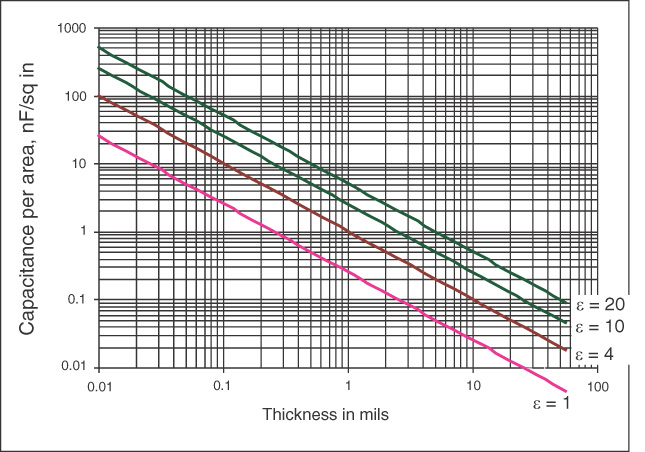
Figure 5-4 Capacitance per area for power and ground planes with four different dielectric constants and different plane-to-plane thicknesses.
An example of such a material is in development by 3M, under the trade name C-Ply. It is composed of ground-up barium titanate in a polymer matrix. The dielectric constant is 20, and the layer thickness is 8 microns, or 0.33 mil. With ½-ounce copper layers laminated to each side, the capacitance per area of one layer is C/A = 0.225 pF/inch × 20 /0.33 mil ~ 14 nF/in2. This is about 30 times greater than the best alternative.
A 4-in 2 region of a board with a layer of C-Ply would have about 56 nF of decoupling capacitance. For the 1-watt chip, this would provide decoupling for about 28 nsec, a significant amount of time.
5.6 Capacitance per Length
Most uniform interconnects have a signal path and a return path with a fixed cross section. In this case, the capacitance between the signal trace and its return path scales with the length of the interconnect. If the interconnect length doubles, the total capacitance of the trace will double. It is convenient to describe the capacitance of the line by the capacitance per length. As long as the cross section remains uniform, the capacitance per length will be constant.
In the special case of uniform cross-section interconnects, the total capacitance between the signal and return path is related to:
where:
C = total capacitance of the interconnect
CL = capacitance per length
Len = length of the interconnect
There are three cross sections for which Maxwell’s Equations can be solved in cylindrical coordinates exactly (see Figure 5-5). For these structures, the capacitance per length can be calculated exactly based on the cross section. They are good calibration structures to test any field solver. In addition, there are many other approximations for other geometries, but they are approximations.

Figure 5-5 The three cross-section geometries for which there are very good approximations for the capacitance per length: coax, twin rods, and rod over plane.
TIP
In general, when the cross section is uniform, a 2D field solver can be used to very accurately calculate the capacitance per length of any arbitrary shape.
A coax cable is an interconnect with a central round conductor surrounded by dielectric material and then enclosed by an outer round conductor. The center conductor is usually termed the signal path, and the outer conductor is termed the return path. The capacitance per length between the inner conductor and the outer conductor is given exactly by:

CL = capacitance per length
ε0 = permittivity of free space = 0.089 pF/cm, or 0.225 pF/inch
εr = relative dielectric constant of the insulation
a = inner radius of the signal conductor
b = outer radius of the return conductor
For example, in an RG58 coax cable (the most common type of coax cable, typically with BNC connectors on the ends), the ratio of the outer to the inner diameters is (1.62 mm/0.54 mm) = 3, with a dielectric constant of 2.3 for polyethylene, the capacitance per length is:

A second exact relationship is for the capacitance between two parallel rods. It is given by:

where:
CL = capacitance per length
ε0 = permittivity of free space = 0.089 pF/cm, or 0.225 pF/inch
εr = relative dielectric constant of the insulation
s = center-to-center separation of the rods
r = radius of the two rods
If the spacing between the rods is large compared with their radius (i.e., s >> r), this relatively complex relationship can be approximated by:

Both cases assume that the dielectric material surrounding the two rods is uniform everywhere. Unfortunately, this is not often the case, and this approximation is not very useful except in special cases, such as wire bonds in air. For example, two parallel wire bonds, both of radius 0.5-mil and 5-mil center-to-center separation, have a capacitance per length of about:

If they are 40 mils long, the total capacitance is 0.3 × 0.04 = 0.012 pF.
The third exact relationship is for a rod over a plane. The capacitance, when the rod is far from the plane (i.e., h >> r), is approximately:

where:
CL = capacitance per length
ε0 = permittivity of free space = 0.089 pF/cm, or 0.225 pF/inch
εr = relative dielectric constant of the insulation
h = center of the rod to surface of the plane
r = radius of the rod
Two other useful approximations for cross sections are commonly found in circuit-board interconnects. These are for microstrip and stripline interconnects, as illustrated in Figure 5-6.

Figure 5-6 The cross-section geometries for microstrip and stripline interconnects illustrating the important geometrical features.
In microstrip interconnects, a signal trace rests on top of a dielectric layer that has a plane below. This is the common geometry for surface traces in a multilayer board. In a stripline, two planes provide the return path on either side of the signal trace. Whether or not the two planes actually have a DC connection between them, for high-frequency signals, they are effectively shorted together and can be considered connected. A signal trace is symmetrically spaced between them. A dielectric material, the board laminate, completely surrounds the signal conductors. In both cases, the capacitance per length between the signal trace and return path is calculated.
Though many approximations exist in the literature, the two offered here are recommended by the IPC, the industry association for the printed circuit board industry. The capacitance per length of a microstrip is given by:
where:
CL = capacitance per length, in pF/inch
εr = relative dielectric constant of the insulation
h = dielectric thickness, in mils
w = line width, in mils
t = thickness of the conductor, in mils
It is important to keep in mind that though there is a parameter to include the thickness of the trace, if a problem requires the level of accuracy where the impact from the trace thickness is important, this approximation should not be used. Rather, a 2D field solver should be used. For all practical purposes, the accuracy of this tool will not be affected if the trace thickness is assumed to be 0.
If the line width is twice the dielectric thickness (i.e., w = 2 × h), and the dielectric constant is 4, the capacitance per length is about CL = 2.7 pF/inch. These are the dimensions of a microstrip that is approximately a 50-Ohm transmission line.
The capacitance per length of a stripline, as illustrated in Figure 5-6, is approximated by:

where:
CL = capacitance per length in pF/inch
εr = relative dielectric constant of the insulation
b = total dielectric thickness, in mils
w = line width, in mils
t = thickness of the conductor, in mils
For example, if the total dielectric thickness, b, is twice the line width, b = 2w, corresponding to roughly a 50-Ohm line, the capacitance per length is CL = 3.8 pF/inch.
In both geometries, we see that the capacitance per length of a 50-Ohm line is about 3.5 pF/inch. This is a good rule of thumb to keep in mind.
TIP
As a rough rule of thumb, the capacitance per length of a 50-Ohm transmission line in FR4 is about 3.5 pF/inch.
For example, in a multilayer BGA package, signal traces are designed as microstrip geometries and are roughly 50-Ohm characteristic impedance. The dielectric material bismaleimide triazine (BT), has a dielectric constant of about 3.9. The capacitance per length of a signal trace is roughly 3.5 pF/inch. A trace that is 0.5 inch long will have a capacitance of about 3.5 pF/inch × 0.5 inch = 1.7 pF. The capacitive load of a receiver would be approximated as the roughly 2 pF of input-gate capacitance and the 1.7 pF of the lead capacitance, or about 3.7 pF.
TIP
It is important to keep in mind that these approximations are approximations. If it is important to have confidence in the accuracy, the capacitance per length should be calculated with a 2D field solver.
5.7 2D Field Solvers
When accuracy is important, the best numerical tool to use to calculate the capacitance per length between any two conductors is a 2D field solver. These tools assume that the cross section of the conductors is constant down their length. When this is the case, the capacitance per length is also constant down the length.
A 2D field solver will solve LaPlace’s Equation, one of Maxwell’s Equations, using the geometry of the conductors as the boundary conditions. The process that most tools use, without the user really needing to know, is to set the voltage of one conductor to be 1 volt and solving for the electric fields everywhere in the space. The charge on the conductors is then calculated from the electric fields. The capacitance per length between the two conductors is directly calculated as the ratio of the charge on the conductors per the 1 v applied.
One way of evaluating the accuracy of a 2D field solver is to use the tool to calculate a geometry for which there is an exact expression, such as a coax or twin-rod structure. For example, Figure 5-7 shows the comparison of the capacitance per length calculated by a field solver for the twin-rod structure, compared to the exact expression above. The agreement is seen to be excellent. To quantify the residual error, the relative difference between the field-solver result and the analytic result is plotted. The worst-case error is seen to be less than 1% for this specific tool.

Figure 5-7 Calculated capacitance per length of twin rods, comparing Ansoft’s 2D Extractor field solver and the exact formula and the approximation. Top: The points are from the field solver; the line through them is the exact expression, and the other line is the approximation. For s > 4r, the approximation is excellent. Bottom: Absolute error of the Ansoft 2D field solver is seen to be better than 1%.
TIP
For any arbitrary geometry, it is possible to get better than 1% absolute error by using a field solver to calculate the capacitance per length.
Using a field solver whose accuracy has been verified, it is interesting to evaluate the accuracy of some of the popular approximations, such as the capacitance per length for a microstrip or stripline structure.
Figure 5-8 compares the approximation above for a microstrip and the field-solver result. In some cases, the approximation can be as good as 5%, but in other cases, the results differ by more than 20%. No approximation should be relied on for better than 10%–20% unless previously verified.

Figure 5-8 Calculated capacitance per length of a microstrip with 5-mil-thick dielectric, and dielectric constants of 4 and 1, comparing Ansoft’s SI2D field solver and the IPC approximation above, as the line width is increased. Circles are the field-solver results; the lines are the IPC approximation.
An additional advantage of using a field solver is the ability to take into account second-order effects. One important effect is the impact from increasing trace thickness on the capacitance per length for a microstrip.
Before we blindly use the field solver to get a result, we should always apply rule 9 and anticipate what we expect to see.
As the metal thickness increases, from very thin to very thick, the fringe fields between the signal line and the return plane will increase. In fact, as shown in Figure 5-9, the capacitance per length does increase with increasing trace thickness, but not very much. It increases only about 3% from very thin to 3 mils thick, or 2-ounce copper.

Figure 5-9 Effect on capacitance per length of a microstrip as the trace thickness is increased from 0.1 mil to 5 mils with 5-mil-thick dielectric and 10-mil-wide conductor. Circles are the field-solver results; the line is the IPC approximation.
There are no approximations that can accurately predict these sorts of effects. For comparison, we show how the IPC approximation for the capacitance matches the more accurate field-solver results. The poor agreement is the reason the approximation should not be used to evaluate the impact of second-order effects, such as trace thickness.
A 2D field solver is a very important tool for calculating the electrical properties of any uniform cross-section interconnect. It is especially important when the dielectric material is not homogeneously distributed around the conductors.
5.8 Effective Dielectric Constant
In any cross section where the dielectric material completely surrounds the conductors, all the field lines between the conductors will see the same dielectric constant. This is the case for stripline, for example. However, if the material is not uniformly distributed around the conductors, such as with a microstrip or twisted pair or coplanar, some field lines may encounter air, while other field lines encounter the dielectric. An example of the field lines in microstrip is shown in Figure 5-10.
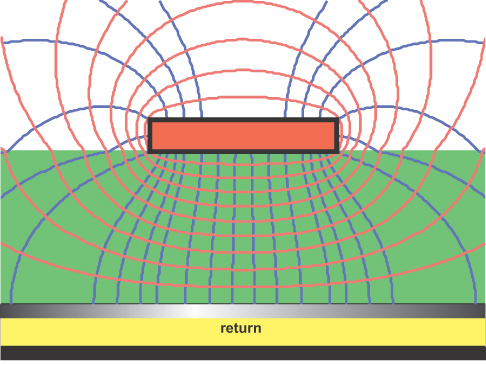
Figure 5-10 Field lines in a microstrip showing some in air and some in the bulk material. The effective dielectric constant is a combination of the dielectric constant of air and the bulk dielectric constant. Field lines calculated using Mentor Graphics HyperLynx.
The presence of the insulating material will increase the capacitance between the conductors compared to if the material was not there. When the material is homogeneously distributed between and around the conductors, such as in stripline, the material will increase the capacitance by a factor equal to the dielectric constant of the material.
In microstrip, some of the field lines encounter air, and some encounter the dielectric constant of the laminate. The capacitance between the signal path and the plane will increase due to the material between them—but by how much?
The combination of air and partial filling of the dielectric creates an effective dielectric constant. Just as the dielectric constant is the ratio of the filled capacitance to the empty capacitance, the effective dielectric constant is the ratio of the capacitance when the material is in place with whatever distribution is really there, compared to the capacitance between the conductors when there is only air surrounding them.
The first step in calculating the effective dielectric constant, εeff, is to calculate the capacitance per length between the two conductors with empty space between them, C0. The second step is to add the material as it is distributed and calculate, using the 2D field solver, the resulting capacitance per length, Cfilled. The effective dielectric constant is just the ratio:

where:
C0 = empty space capacitance
Cfilled = capacitance with the actual material distribution
εeff = effective dielectric constant
Both the empty and filled capacitance can be accurately calculated using a 2D field solver. The only accurate way of calculating the effective dielectric constant of a transmission line is by using a 2D field solver. As we show in Chapter 7, “The Physical Basis of Transmission Lines,” the effective dielectric constant is a very important performance term, as it directly determines the speed of a signal in a transmission line.
Figure 5-11 shows the calculated effective dielectric constant for a microstrip as the width of the trace is increased. The bulk dielectric constant in this case is 4. For a very wide trace, most of the field lines are in the bulk material, and the effective dielectric constant approaches 4. When the line width is narrow, most of the field lines are in the air, and the effective dielectric constant is below 3, reflecting the contribution from the lower dielectric constant of air.

Figure 5-11 Effective dielectric constant of a microstrip with a 5-mil-thick dielectric, as the line width is increased. The dielectric constant of the bulk material is 4. Results are calculated with the Ansoft 2D Extractor.
TIP
The intrinsic bulk dielectric constant of the laminate material is not changing. Only how it affects the capacitance changes as the fields between the conductors encounter a different mix of air and dielectric.
If dielectric material is added to the top surface of the microstrip, the fringe field lines that were in air will see a higher dielectric constant, and the capacitance of the microstrip will increase. With dielectric above, we call this an embedded microstrip. When only some of the field lines are in the material, it is called a partially embedded microstrip. This is the case for a soldermask coating, for example. When all the field lines are covered by dielectric, it is called a fully embedded microstrip. Figure 5-12 shows the field line distribution for three different degrees of embedded microstrip.

Figure 5-12 The electric field distribution around a microstrip with different thickness covering. For a thick enough layer, all the fields are confined in the bulk material, and the capacitance will be independent of more thickness. Simulations performed with Mentor Graphics HyperLynx.
How much material would have to be added to a microstrip to completely cover all the field lines and have the bulk dielectric constant match the effective dielectric constant? This is an easy problem to solve with a 2D field solver. Figure 5-13 shows the calculated capacitance per length for a microstrip with 5-mil-thick dielectric and 10-mil-wide trace as a top layer of dielectric is added with the same bulk dielectric constant value as the laminate, 4.

Figure 5-13 Capacitance per length of microstrip as top dielectric thickness is increased. Calculated using Ansoft’s 2D Extractor.
In this example, a thickness of dielectric on top of the trace about equal to the line width is required to fully cover all the fringe fields.
5.9 The Bottom Line
1. Capacitance is a measure of the capacity to store charge between two conductors.
2. Current flows through a capacitor when the voltage between the conductors changes. Capacitance is a measure of how much current will flow.
3. With few exceptions, every formula relating the capacitance of two conductors is an approximation. If better than 10%–20% accuracy is required, approximations should not be used.
4. The only three exact expressions are for coax, twin rods, and rod over ground.
5. In general, the farther apart the conductors, the lower the capacitance. The greater the overlap of their areas, the higher the capacitance.
6. Dielectric constant is an intrinsic bulk-material property that relates how much the capacitance is increased due to the presence of the material.
7. The power and ground planes in a circuit board have capacitance. However, the amount is so small as to be negligible. The value the planes provide is not for their decoupling capacitance but for their low loop inductance.
8. The IPC approximations for microstrip and stripline should not be used if accuracy better than 10% is required.
9. A 2D field solver, once verified, can be used to calculate the capacitance per length of a uniform transmission line structure to better than 1%.
10. Increasing conductor thickness in a microstrip will increase the capacitance per length—but only slightly. A change from very thin to 2-ounce copper only increases the capacitance by 3%.
11. Increasing the thickness of the dielectric coating on top of a microstrip will increase the capacitance. Completely enclosing all the fringe field lines happens when the coating is as thick as the trace is wide and the capacitance can increase by as much as 20%.
12. The effective dielectric constant is the composite dielectric constant when the material is not homogeneously distributed and some field lines see different materials, such as in a microstrip. It can easily be calculated with a 2D field solver.
End-of-Chapter Review Questions
The answers to the following review questions can be found in Appendix D, “Review Questions and Answers.”
5.1 What is capacitance?
5.2 Give one example where capacitance is an important performance metric.
5.3 What are two different interpretations of what the capacitance between two conductors measures.
5.4 A small piece of metal might have a capacitance of 1 pF to the nearest metal, inches away. There is no DC connection between these pieces of metal. At 1 GHz, what is the impedance between these conductors?
5.5 How does conduction current flow through the insulating dielectric of a capacitor?
5.6 What is the origin of displacement current, and where will it flow?
5.7 If you wanted to engineer a higher capacitance between the power and ground planes in a board, what three design features would you change?
5.8 What primary property about the chemistry of a dielectric most strongly influences its dielectric constant?
5.9 What happens to the capacitance between two conductors when the voltage between them increases?
5.10 In a coax geometry, what happens to the capacitance if the outer radius is increased?
5.11 What happens to the capacitance per length in a microstrip if the signal path is moved away from the return path?
5.12 Is there any geometry in which capacitance increases when the conductors are moved farther apart?
5.13 Why does the effective dielectric constant increase as the thickness of the dielectric coating increases in microstrip?
5.14 What is the lowest dielectric constant of a solid, homogenous material? What material is that?
5.15 What could you do to a material to dramatically reduce its dielectric constant?
5.16 What happens to the capacitance per length of a microstrip if solder mask is added to the top surface?
5.17 What happens to the capacitance per length of a microstrip if the conductor thickness increases?
5.18 What happens to the capacitance per length of a stripline if the line width increases?
5.19 What happens to the capacitance per length of a stripline if the trace thickness increases?
5.20 For the same line width and dielectric thickness per layer, which will have more capacitance per length: a microstrip or a stripline?
5.21 What is theoretically the lowest dielectric constant any material could have?
5.22 Why is the capacitance per length constant in a uniform cross section interconnect?
5.23 On die, the dielectric thickness between the power and ground rails can be as thin as 0.1 micron. If the SIO2 dielectric constant is also 4, how does the on-die capacitance per square inch compare to the on-board capacitance per square inch if the power and ground plane separation is 10 mils?
5.24 What is the capacitance between the faces of a penny if they are separated with air?
5.25 What is the minimum capacitance between a sphere 2 cm in diameter suspended a meter above the floor? How does this capacitance change as the sphere is raised higher above the floor?
5.26 What is the capacitance between the power and ground planes in a circuit board if the planes are 10 inches on a side, 10 mils separation, and filled with FR4?
5.27 Derive the capacitance per length of the rod over a plane from the capacitance per length of the twin rod geometry, in air.