
Smart cards, perhaps more than most other technologies, have been subject to tremendous pressures across their lifetime to conform to standard implementation and deployment strategies. The form factor, electrical characteristics, and model of computation are firmly established by internationally recognized standards. This has the attractive benefit of guaranteeing that no one approach can attain a monopoly or near-monopoly stranglehold on the technology (e.g., PC operating systems). However, it does encumber the use of smart cards with a tremendous load of baggage. The chances for true, revolutionary advances are greatly minimized, if not eliminated, by the need to conform to established equipment and operations trails that stretch for decades into the past.
At least three distinct approaches to standardization are present in today's smart card world:
international standards
de facto standards from consortia
patent and copyright protection for Intellectual Property (IP)
The precursors to today's smart cards were the plastic credit cards used as identity tokens in the retail financial marketplace. These tokens, when introduced, represented a significant improvement in the ability of merchants to accept payment in an abstract form (essentially “on credit”) from customers whose identity they could not personally vouch for. The credit card represented (and actually still does) a certification of identity and financial situation from an issuer functioning as a trust broker.
In the trust infrastructure provided by the credit card (although a merchant might not be personally inclined to extend credit to an unknown customer to make a purchase), it was reasonable for the merchant to trust the issuer of a credit card, in no small part because of the known financial strength of the issuer and because of financial agreements entered into when the merchant became “certified” to accept the (credit card) tokens of the card issuer.
As the convenience of credit cards became established and their use spread, it became highly desirable to achieve an unprecedented level of interoperability among cards from different issuers and transaction equipment from a variety of vendors in merchants' stores around the world.
The start of the journey toward worldwide interoperability lay in the establishment of international standards regarding first the cards themselves, and then the equipment that would work with them and with the environments in which they would be used. The venue of choice for establishing such standards was the International Standards Organization (ISO). In some fields of technical activity, the International Electrotechnical Commission (IEC) collaborates with the ISO in the development of standards. Similarly, in the United States, the American National Standards Institute (ANSI) functions as a primary standards-setting body. Consequently, in the following discussion, some standards are ISO standards and others are joint ISO/IEC/ANSI standards accepted by all three bodies.
ISO/IEC (and in some instances, ANSI) standards have been established to fully describe plastic identification cards. The various standards have evolved over time and are found in a variety of ISO/IEC/ANSI classifications, the more pertinent of which are listed in Table 3.1.
Table 3.1. ISO Standards Pertaining to Smart Cards
ISO/IEC Standard | Title |
|---|---|
ISO/IEC 7810 – 1995-08-15 | Identification Cards –. Physical Characteristics |
ANSI/ISO/IEC 7811-1 – 1995: Part 1 | Identification Cards –. Recording Technique Embossing |
ANSI/ISO/IEC 7811-2 – 1995: Part 2 | Identification Cards –. Recording Technique Magnetic Stripe |
ANSI/ISO/IEC 7811-3 – 1995: Part 3 | Identification Cards –. Recording Technique Location of Embossed Characters on ID-1 Cards |
ANSI/ISO/IEC 7811-4 – 1995: Part 4 | Identification Cards –. Recording Technique Location of Read-Only Magnetic Tracks – Tracks 1 and 2 |
ANSI/ISO/IEC 7811-5 – 1995: Part 5 | Identification Cards –. Recording Technique Location of Read/Write Magnetic Tracks – Track 3 |
ANSI/ISO/IEC 7812-1–1993 | Identification Cards –. Identification of Issuers Part 1: Numbering System |
ANSI/ISO/IEC 7813 – 1995 | Identification Cards –. Financial Transaction Cards |
ISO 7816-1 | Identification Cards –. Integrated Circuit(s) Cards with Contacts – Physical Characteristics |
ISO 7816-2 | Identification Cards –. Integrated Circuit(s) Cards with Contacts – Dimensions and Location of the Contacts |
ISO 7816-3 | Identification Cards –. Integrated Circuit(s) Cards with Contacts – Electronic Signals and Transmission Protocols |
ISO 7816-3 Amendment 1 | Protocol Type T=1, Asynchronous Half-Duplex Block Transmission Protocol |
ISO 7816-3 Amendment 2 | Revision of Protocol Type Selection |
ISO 7816-4 | Identification Cards –. Integrated Circuit(s) Cards with Contacts – Inter-Industry Commands for Interchange |
ISO 7816-5 | Identification Cards –. Integrated Circuit(s) Cards with Contacts – Number System and Registration Procedure for Application Identifiers |
ISO 7816-6 | Identification Cards –. Integrated Circuit(s) Cards with Contacts – Inter-Industry Data Elements |
ISO 1177 - 1985 | Information Processing –. Character Structure for Start/Stop and Synchronous Character-Oriented Transmission |
A seminal specification that ultimately leads to smart cards is ISO/IEC 7810: Identification Cards—Physical Characteristics. This standard defines nominal physical characteristics for three types of identification cards, labeled ID-1, ID-2, and ID-3. Card type ID-1 deals with the generally accepted size and shape of a credit card or smart card and is the primary focus of this discussion. The ID-2 and ID-3 card types are simply larger sizes, but with all the other physical characteristics the same as ID-1 card types.
The basic function of an ID-1 identification card is to contain information in a visual, tactile, and electronic form that identifies its bearer and that may support transactions the card is to enable. Visual information may be presented through artwork, personal pictures, anti-counterfeiting mechanisms such as holograms, or machine-readable mechanisms such as bar codes. Embossing is used to convey information in a tactile form suitable for creating impressions of characters on other media, a capability often used in transactions based on such identification cards. Information may be conveyed in electronic form through two mechanisms: magnetic stripes, which are prevalent on credit cards, and an embedded integrated circuit chip (ICC), which is the defining characteristic of smart cards.
The elements of an ID-1 identification card include:
the card backing (the plastic)
optional embossing areas on which alphanumeric information may be stamped
an optional area to which a magnetic stripe may be attached
Information then can be magnetically encoded on the magnetic stripe. As illustrated in Figure 3.1, an ID-1 identification card is a rectangle 85.6 mm wide, 53.98 mm tall, and 0.76 mm thick. ISO/IEC 7810 places stringent restrictions on the distortions allowed in the card backing, particularly near the area that might contain a magnetic stripe. The intent of these exacting specifications is to ensure that reader or imprinting devices that ID-1 cards are inserted into can be expected to reliably read the information off a magnetic stripe and imprint the embossed numerals reliably without causing any damage or significant deterioration of the card.

The material characteristics of ID-1 identification cards are also established by ISO/IEC 7810; specifically, the card must be composed of polyvinyl chloride (PVC), PVC acetate, or “materials having equal or better performance.” There are correspondingly stringent deformation characteristics for the card. In general, the specifications require that after one end of a card is flexed by up to 35 mm (which corresponds to about half the width of a card), it should return to its original flat state to within 1.5 mm. Further, it is specified that it be possible to bring the card to within an acceptable flat state through the uniform application of a moderately light pressure across the face of the card. Interestingly, the actual durability of a card is not established by the ISO/IEC specifications, but rather is left to a “mutual agreement between the card issuer and the manufacturer.”
Building on the base formed by ISO/IEC 7810, the ANSI/ISO/IEC 7811 specification establishes standards for the encoding of information on an identification card through embossing or magnetic stripe techniques. This specification is divided into five parts:
embossing (recording technique)
magnetic stripe (recording technique)
location of embossed characters on ID-1 cards
location of read-only magnetic tracks (tracks 1 and 2)
location of read-write magnetic track (track 3)
Embossing means causing the shape of characters to rise above the backing plane of the card. The embossed characters essentially form a typeface that can be used to print these characters onto some other material through the use of a rudimentary “printing press”: before online printing of transaction receipts became prevalent, merchants used these credit card imprinting devices to prepare credit card invoices and receipts. ANSI/ISO/IEC 7811-1 establishes the allowed characteristics of embossing itself, including the relief height of the embossed characters (0.46 mm to 0.48 mm), the spacing between embossed characters (2.54 mm to 3.63 mm), and the size of the characters (4.32 mm). Auxiliary ISO specifications identify the characters and font sizes that render embossed characters suitable for optical recognition devices, along with the test procedures to be used to determine that a specific identification card meets all of these specifications; these include:
ISO 1073-1, Alphanumeric character sets for optical recognition–Part 1: Character set OCR-A–Shapes and dimensions of the printed image.
ISO 1073-2, Alphanumeric character sets for optical recognition–Part 2: Character set OCR-B–Shapes and dimensions of the printed image.
ISO 1831, Printing specifications for optical character recognition.
ISO/IEC 10373, Identification cards–Test methods.
ANSI/ISO/IEC 7811-2 specifies the recording techniques to be used to encode characters into a magnetic stripe affixed to an ID-1 card. Provisions are made for three different types of information recording, referenced as Track 1, Track 2, and Track 3. Track 1 can contain up to 79 alphanumeric characters encoded at a write density of 8.27 bits per mm (210 bits per inch); this track can contain both alphabetic and numeric information. Track 2 can contain up to 40 characters of numeric information encoded at a write density of 2.95 bits per mm (75 bits per inch). Both Track 1 and Track 2 are intended to be write-once/read-many channels; essentially, once the card is issued, these are read-only channels. Track 3 is both a write-many and a read-many facility (that is, a read/write track). It can contain up to 107 characters encoded at 8.27 bits per mm (210 bits per inch). The encoding for each of the data tracks includes a “longitudinal redundancy check” character that can be used by the card reader to detect any errors in the information read versus what was originally written onto the card.
ANSI/ISO/IEC 7811-3 specifies in detail the location of embossed characters on an ID-1 card, and Part 4 specifies the location of magnetic stripes. As illustrated in Figure 3.2, two areas for embossing are specified. The first, whose center line is 21.42 mm above the bottom edge of the card, or just below the center line of the card, allows for up to 19 card identification number numerals to be embossed. Just below this is an additional area of approximately 14.53 mm × 66.04 mm in which 4 rows of 27 characters each can be used to form a name and address field, which is offset at least 2.41 mm from the bottom of the card and 7.65 mm from the left edge. The embossed characters are raised toward the front side of the card. If a magnetic stripe is included on the card, it is found near the top, on the back side of the card. The specifications state that the magnetic stripe and the embossing may not overlap.

Two variants of magnetic stripes can be found on ID-1 identification cards; the form and location of these are defined in ANSI/ISO/IEC 7811-4 (for read-only tracks) and Part 5 (for read/write tracks). One of these is 6.35 mm tall × 79.76 mm wide, positioned no more than 5.54 mm from the top edge of the card and on the back face of the card. This magnetic stripe supports two recording tracks, each of which is intended to be a read-only track.
By following the ISO standards through several interconnected specifications for identification cards, it is possible to go beyond just the description of physical and electronic characteristics of the card, arriving at a business model from which inferences can be made regarding how cards will be manufactured, what groups will actually distribute the cards to end-users, and some of the operations to be performed by the end-users of the identification cards. For example, the ANSI/ISO/IEC 7811-1 specification defines two terms reflecting the distribution state of a card:
Unused card. A card that has been embossed with all the characters required for its intended purpose but has not been issued.
Return card. An embossed card after it has been issued to the cardholder and returned for the purpose of testing.
ANSI/ISO/IEC 7811-2 further defines similar states for magnetic stripe cards:
Unused unencoded card. A card possessing all components required for its intended purpose that has not been subjected to any personalization or testing operation. The card has been stored in a clean environment without more than 48-hour exposure to daylight at temperatures between 5 degrees C and 30 degrees C and humidity between 10% and 90%, without experiencing thermal shock.
Unused encoded card. An unused, unencoded card that has only been encoded with all the data required for its intended purpose (for example, magnetic encoding, embossing, electronic encoding).
Returned card. An embossed and/or encoded card after it has been issued to the cardholder and returned for the purpose of testing.
ANSI/ISO/IEC 7812: “Identification of Issuers—Part 1: Numbering System” further develops the business model by establishing a standard for the card identification number, which is displayed in embossed characters on the front face of an ID-1 card. The card identification number, which may be up to 19 characters long, is subdivided into three components:
Issuer identification number. A six-digit component that includes the following:
Major industry identifier. A one-digit indicator of the industry designation of the card issuer; it is one of the following:
0 -. Tag reserved to indicate new industry assignments
1 -. Airlines
2 -. Airlines and other future industry assignments
3 -. Travel and entertainment
4 -. Banking/financial
5 -. Banking/financial
6 -. Merchandizing and banking
7 -. Petroleum
8 -. Telecommunications and other future industry assignments
9 -. For assignment by national standards bodies
Issuer identifier -. A five-digit number associated with the specific issuing organization
Individual account identification number. A variable-length component up to 12 digits maximum.
Check digit. A cross-check number that is calculated from all the previous digits in the identification number according to an algorithm called the Luhn formula that is defined in an appendix of ANSI/ISO/IEC 7812.
The path toward standards-based specification of a general business mode (for financial transactions) becomes very explicit with ISO/IEC 7813: Identification Cards— Financial Transaction Cards. This specification does not consider any new technical areas, but makes a strict enumeration of the standards that must be adhered to in order to call a card a financial transaction card.
ISO/IEC 7813 specifies the content of the two read-only tracks of a magnetic stripe included on the card; this augments the content definition for ISO 4909 for the read/write track. The end result is a complete description of both the technical characteristics and the information content of cards suitable to support financial transactions, all rooted in international standards and acceptable for worldwide deployment.
ISO 7816: Identification Cards — Integrated Circuit(s) Cards with Contacts provides the basis to transition the relatively simple identification card from a token that can be compromised through forgery, theft, or loss into a tamper-resistant and “intelligent” integrated circuit chip (ICC) card, more popularly known as a smart card. It is a multiple-part standard through which the smart card is specified in sufficient detail to achieve the same level of interoperability that has been achieved with the simpler cards discussed in the section “ISO Standards for Cards.” Although ISO 7816 includes many approved parts and has several additional parts under review, the discussion here is aimed primarily at Parts 1 through 5. Consideration of other parts of ISO 7816 will occur in various later chapters.
Part 1 -. Physical characteristics
Part 2 -. Dimensions and location of the contacts
Part 3 -. Electronic signals and transmission protocols
Part 3, Amendment 2 -. Revision of protocol type selection
Part 4 -. Inter-industry commands for interchange
Part 5 -. Numbering system and registration procedure for application identifiers
Note
In the ISO standards related to ICCs, the device into which the ICC is inserted is referred to as an interface device (IFD). In the course of this book, the terms ICC, card, and smart card tend to be used interchangeably. Similarly, the terms IFD, reader, and terminal are used to mean the same thing.
ISO 7816-1 extends the physical characteristics definition of simpler ID-1 identification cards from the realm of plastic cards with perhaps an associated magnetic stripe to the more complex environment supporting an ICC within the card. This includes accommodation of exposure limits for a number of electromagnetic phenomena such as x-rays, ultraviolet light, electromagnetic fields, static electrical fields, and ambient temperature of the card (with embedded chip), as indicated in Table 3.2.
Table 3.2. Exposure Limits for Physical Phenomena
Phenomenon | Limit |
|---|---|
Ultraviolet light | Ambient (depends on card vendor) |
X-rays | Two times acceptable annual human dosage |
EMI (electromagnetic interference) | No interference with magnetic stripe |
Electromagnetic fields | Less than 1,000 Oe |
Static electricity | 1,500-volt (v) discharge through 1.5-K ohm resistor from 100-pF capacitor |
Heat dissipation | Less than 2.5 watt; card temperature less than 50º C |
The specification is also concerned with defining the characteristics of the card when it is bent or flexed. The concern, of course, is that an environment amenable to operation of the chip in the card—with its microelectronic connections between surface connectors and chip I/O pins, as well as its integrated circuitry—be maintained. Two tests of flexibility for the card are specified: Figure 3.3 illustrates the bending requirements of the card and Figure 3.4 illustrates the torsion requirements of the card.


In the cases of both bending tests and torsion tests, the concern is that through the normal wear and tear on a card (e.g., keeping the card in one's wallet), either the chip itself or the microconnection wires from the chip to the surface contacts will be damaged or broken. Practical experience with these tests has shown that a chip size on the order of 25 mm2 is the largest that can routinely meet these flexibility constraints.
The mechanical tolerances required of smart cards are relatively stringent in order to ensure that cards can be properly aligned such that a reader's contact points can make a good electrical connection with the correct card contacts. In general, the card's contacts cannot vary from the surface of the card by more than 0.1 mm. The card must be sufficiently strong to resist permanent deformation when bent; it must be possible to return the card to a flat position with a very modest pressure over the face of the card. Finally, the electrical resistance of the card's contacts must fall within the acceptable limits established by ISO 7816-1.
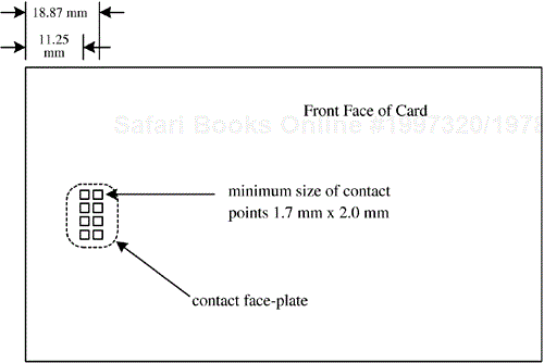
ISO 7816-2 specifies an ICC with eight electrical contacts present in a standardized position on the front face of the card; these are referred to as C1 through C8. Some of these contacts are electrically connected to the microprocessor chip embedded within the card; some are not, having been defined to allow for enhancements but unused at the present time. The specific definitions for the contacts are shown inTable 3.3.
Table 3.3. Contact Definitions for Smart Cards
Contact | Designation | Use |
|---|---|---|
C1 | Vcc | Power connection through which operating power is supplied to the microprocessor chip in the card. |
C2 | RST | Reset line through which the IFD can signal to the smart card's microprocessor chip to initiate its reset sequence of instructions. |
C3 | CLK | Clock signal line through which a clock signal can be provided to the smart card's microprocessor chip to control the speed at which it operates and to provide a common framework for data communication between the reader and the smart card. |
C4 | RFU | Reserved for future use. |
C5 | GND | Ground line providing a common electrical ground between the reader and the smart card. |
C6 | Vpp | Programming power connection providing a separate source of electrical power (from the operating power) that can be used to program the NVM on the microprocessor chip. |
C7 | I/O | Input/output line that provides a half-duplex communication channel between the reader and the smart card. |
C8 | RFU | Reserved for future use. |
The location of the contacts is illustrated in Figure 3.5. The contacts are almost always found on the front face of the card (which is the side of the card with the primary graphic and opposite the side with any magnetic stripe). However, the ISO 7816-2 standard does not mandate that the contacts appear on the front; the contacts can appear on the back of the card as long as care is taken to make sure the contacts do not intersect the magnetic stripe area.
Many of the earliest smart cards adhered to a different standard for contact locations that positioned the contacts toward the upper-left portion of the front face of the card. The standard on which this positioning was based became obsolete in 1990. Cards designed according to this standard were deployed primarily in Europe to support credit and debit applications.
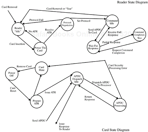
ISO 7816-3 begins to delve into the specification of the “intelligent” aspects of the smart card. This standard describes the relationship between the smart card and the reader as one of “slave” (the smart card) and “master” (the reader). Communications are established by the reader signaling to the smart card through the contacts noted previously and are continued by the smart card responding accordingly. Communication between the card and reader proceed according to various state transitions illustrated in Figure 3.6. The communication channel is single-threaded; once the reader sends a command to the smart card, it blocks until a response is received.
When a card is inserted into a reader, no power is applied to any of the contacts. The chip on the card could be seriously damaged by applying power to the wrong contacts, and this situation could easily occur if a card were inserted across powered contact points. The contacts remain unpowered until an edge detector determines that the card is properly aligned with the contact points to within some acceptable (for the reader) mechanical tolerance.
Note
Security mechanisms on many chips could be triggered if the cards were inserted across powered contact points, resulting in the possible disabling of the chip.
When the reader detects that the card is properly inserted, power is applied to the card. First, the contacts are brought to a coherent idle state, as shown in Table 3.4; then, a reset signal is sent to the card via the RST contact line. The idle state is characterized as being when the power (VCC) contact is brought up to a normal, stable operating voltage of 5 v; an initial power setting of 5 v is always applied first, even though some microprocessor chips being introduced operate at 3 v when in an I/O state. The I/O contact is set to a reception mode on the reader side and a stable clock (CLK) is applied. The reset line is in a low state. It must remain in a low state for at least 40,000 CLK cycles before a valid reset sequence can be started by the reader raising the reset line to a high state.
As illustrated in Figure 3.7, powering up a smart card occurs according to a well-defined sequence. Once power has been satisfactorily applied to the card, the RST line is raised to a high state that signals to the card to begin its initialization sequence. The specific initialization operations can vary from card to card, but the sequence should result in the sending of an answer to reset (ATR) from the card back to the reader. In general, the first byte of the ATR must be received by the reader within 40,000 clock cycles. Following that, each successive byte of the ATR must be received by the reader at a rate of at least 1 byte per second.

Table 3.4. Contact States Prior to Card Reset
Contact | State |
|---|---|
VCC | Powered and stable |
VPP | Stable at idle state |
RST | State – low |
CLK | Suitable and stable clock signal applied |
I/O | Reception mode in interface device |
Data transfer between the reader and the card occurs through the concerted action of two of the contact lines: CLK and I/O. The I/O line conveys a single bit of information per unit of time as defined by the CLK depending on its voltage relative to GND. One bit can be conveyed either through a +5 v value or through a 0 v value. The actual convention used is determined by the card and is conveyed to the reader's initial character of the ATR, which is referenced as TS. To transfer 1 byte of information, 10 bits are actually moved across the I/O line; the first is always a start bit and the last is always a parity bit used to convey even parity. Considering that the I/O line can be (in one bit period) either in a high (H) state or a low (L) state, the TS character being of the form HLHHLLLLLLH signals that the card wants to use the inverse convention, meaning that H corresponds to a 0 and L corresponds to a 1. A TS character of the form HLHHLHHHLLH signals that the card wants to use the direct convention, meaning that H corresponds to a 1 and L corresponds to a 0.
The direct convention and the inverse convention also control the bit ordering with each byte transferred between the card and the reader. In the direct convention, the first bit following the start bit is the low-order bit of the byte. Successively higher order bits follow in sequence. In the inverse convention, the first bit following the start bit is the high-order bit of the byte. Successively lower order bits follow in sequence. Parity for each byte transferred should be even; this means that the total number of 1 bits in the byte, including the parity bit, must be an even number.
The I/O line comprises a half-duplex channel; that is, either the card or the reader can transmit data over the same channel, but they both cannot be transmitting at the same time. So as part of the power-up sequence, both the reader and the card enter a receive state in which they're listening to the I/O line. With the commencement of the reset operation, the reader remains in the receive state while the card must enter a send state in order to send the ATR back to the reader. From this point on, the two ends of the channel alternate between send states and receive states. With a half-duplex channel, there is no reliable way for either end to asynchronously change a state from send to receive or from receive to send. Rather, if this is desired, that end must go into a receive state and allow a timeout of the operation in progress; then a reader end will always try to re-establish a known sequence by re-entering a send state.
The CLK and I/O lines can support a rather wide variety of data transmission speeds. The specific speed is defined by the card and is conveyed back to the reader through an optional character in the ATR. The transmission speed is set through the establishment of one bit time on the I/O line, which means that an interval is established at which the I/O line may be sampled in order to read a bit and then each successive bit. This time is defined as an elementary time unit (etu) and is established through a linear relationship between several factors. Note that the TS character was returned before any definition of the etu could be made; this is possible because the etu during the ATR sequence is always specified to be
etu0 = 372/(CLK frequency)
where the CLK frequency is always between 1 MHz and 5 MHz; in fact, the frequency is almost always selected such that the initial data transfer rate is 9,600 bps.
Once an RST signal is sent from the reader to the card, the card must respond with the first character of the ATR within 40,000 CLK cycles. The card might not respond with an ATR for a number of reasons, the most prevalent being that the card is inserted incorrectly into the reader (probably upside down). In some instances, the card might not be functioning because it has been damaged or broken. Whatever the case, if the ATR is not returned within the prescribed time, the reader should begin a sequence to power down the card. During this sequence, the reader sets the RST, CLK, and I/O lines low and drops voltage on the VCC line to nominal 0 (that is, less than 0.4 v).
The ATR is a string of characters returned from the card to the reader following the successful completion of the power-up sequence. As defined in ISO/IEC 7816-3, the ATR consists of 33 or fewer characters comprising the following elements:
TS. A mandatory initial character.
T0. A mandatory format character.
TAi TBi TCi TDI. Optional interface characters.
T1, T2, ~TK. Optional historical characters.
TCK. A conditional check character.
The historical characters can be defined at the discretion of the card manufacturer of the card issuer. These characters are typically used to convey some type of designation of the type, model, and use of this specific card. When used in this way, the historical characters provide a modest mechanism through which systems can automatically detect the use to be made of an inserted card (within that system) and can initiate other actions (or software) accordingly. The check character provides a mechanism through which the integrity of the ATR can be measured, that is, whether a transmission error has occurred in sending the characters from the card to the reader.
The structure of the ATR is illustrated in Table 3.5. As discussed previously, the initial TS character is used to establish the bit-signaling and bit-ordering conventions to be used between the reader and the card. The T0 character is used to signal the presence or absence of subsequent interface characters or historical characters. The interface characters are used to tailor the characteristics of the I/O channel, including the specific protocol to be used by the card and reader during subsequent exchange of commands (from the reader to the card) and responses (from the card to the reader). The historical characters, if present, are used to convey card manufacturer–specific information from the card to the reader, and hence to the application system being served by the reader. There is really no established standard for the information presented in the historical bits.
Table 3.5. The Answer to Reset Structure
Character ID | Definition |
|---|---|
Initial Character Section | |
TS | Mandatory initial character |
Format Character Section | |
T0 | Indicator for presence of interface characters |
Interface Characters Section | |
TA1 | Global, codes F1 and D1 |
TB1 | Global, codes 11 and P11 |
TC1 | Global, code N |
TD1 | Codes Y2 and T |
TA2 | Specific |
TB2 | Global, code P12 |
TC2 | Specific |
TD2 | Codes Y3 and T |
TA3 | Tai, Tbi, and Tci are specific |
TDi | Codes Yi+1 and T |
Historical Character Section | |
T1 | (Maximum of 15 characters) |
…TK | Card-specific information |
Check Character Section | |
TCK | Optional check character |
The interface characters are used as a selection method for the protocol to be used for subsequent higher level communication between the reader and the card. Two such protocols are defined by ISO 7816-3: the T=0 protocol and the T=1 protocol. T=0 is an asynchronous protocol, meaning that there is no strict timing connection between one command sent from the reader to the card and the next command sent from the reader to the card. When the card receives a command from the reader, it performs the requested operations and sends back to the reader a response relative to that command. The reader is then free to send the next command to the card whenever it needs to. The T=1 protocol is an asynchronous block transmission protocol. This means that in one transmission packet (from the reader to the card), from one to several commands are sent. The card responds to this (these) command(s), at which point the reader can send another command or block of commands. Designations for additional protocols are defined as indicated in Table 3.6.
Table 3.6. Protocol Designations
Designation | Definition |
|---|---|
T=0 | Asynchronous (single) command/response protocol |
T=1 | Asynchronous (multiple) command/response protocol |
T=2 | Reserved for future full-duplex protocol |
T=3 | Reserved for future full-duplex protocol |
T=4 | Reserved for enhanced asynchronous protocol |
T=5 | Reserved for future use |
T=6 | Reserved for future use |
T=7 | Reserved for future use |
T=8 | Reserved for future use |
T=9 | Reserved for future use |
T=10 | Reserved for future use |
T=11 | Reserved for future use |
T=12 | Reserved for future use |
T=13 | Reserved for future use |
T=14 | Reserved for vendor-defined protocol |
T=15 | Reserved for future extension |
The ATR sequence that initializes the physical communication channel between the reader and the card allows a number of characteristics of the channel to be defined or manipulated. The ISO/IEC 7816-3 standard defines a more elaborate adjunct to the ATR sequence called the Protocol Type Selection (PTS) facility. Actually, the PTS can be thought of as an extension of the ATR. Through the PTS, the reader-side of the channel and the card-side of the channel can negotiate to an optimum set of characteristics for the channel. For most current smart card systems, there is a strong correlation between the reader-side development and the card development. Consequently, the optimum communication characteristics are almost always derived through the ATR sequence without performing a PTS sequence. Therefore, we will not delve into the details of the PTS. However, in the future, with an expanding marketplace for smart cards encouraging more disconnected development of readers, terminals, and cards, the need to go through a PTS sequence on card initialization may significantly increase.
ISO 7816 is unquestionably the most widely known and followed general-purpose smart card standard, but it is by no means the only one. There are standards for the use of smart cards in specific applications such as health, transportation, banking, electronic commerce, and identity. And there are standards for new kinds of smart cards, such as proximity and contactless smart cards. Because a smart card is always part of a larger information technology, it is subject to a wide range of information-processing standards such as character sets, country encodings, monetary representations, and cryptography. Finally, since many smart card applications intersect a number of governmental concerns such as monetary systems, national identity, and benefit eligibility, there are national and regional smart card standards in addition to international standards.
Due to the deliberate pace of international standards efforts, there also is a growing number of smart card specifications issued by organizations such as governmental laboratories, professional societies, trade associations, academic institutions, and private firms not associated with standards bodies. These specifications have no force other than the force of the marketplace of products and ideas, but they do serve the useful role of stimulating discussion and discovering consensus, which can be fed into official standards efforts. As smart cards become embraced within other technologies such as cellular telephones, watches, automobiles, and Internet browsers, we can expect that these technologies and their application domains will make rules and regulations about the nature of the smart card component. For the near term, as smart card usage explodes, it probably will be as much the marketplace as it is the international standards process that will say how smart cards are supposed to be.
As by no means an exhaustive list but rather to simply give you some starting points for further search, Tables 3.7 and 3.8 list some further standards and specifications that are influencing the deployment and evolution of smart cards.
Table 3.7. Examples of Smart Card Standards
Standard | Subject Area |
|---|---|
ISO 639 | Languages, countries, and authorities |
ISO 646 | 7-bit coded character set |
ISO 3166 | Names of countries |
ISO 4217 | Currencies and funds |
ISO/IEC 7501 | Travel documents |
ISO/IEC 7810, 7811, 7812 | Magnetic stripe cards |
ISO/IEC 7813 | Financial transactions |
ISO 8601 | Dates and times |
ISO 8859 | 8-bit coded character set |
ISO 9564 | Personal identification number (PIN) management |
ISO 9797 | Data cryptographic techniques |
ISO 9992 | Messages between card and terminal |
ISO 10202 | Financial transaction cards |
ISO 10536 | Contactless ICCs |
ISO 11568 | Cryptographic key management |
ISO 11694 | Optical memory cards |
European Telecommunications Standards Institute (ETSI) | |
ETSI TE9 | Card terminals |
ETSI TS 102.221 | UICC-Terminal Interface; Physical and Logical Characteristics |
ETSI TS 102.222 | Administrative Commands for Telecommunications Applications |
ETSI TS 102.223 | Card Application Toolkit |
ETSI TS 102.240 | UICC Application Programming Interface |
Third Generation Partnership Project (3GPP) | |
3GPP TS 31.113 | USAT Interpreter Byte Codes |
3GPP TS 31.131 C | Language Binding to the (U)SIM API |
3GPP TS 43.019 | SIM API for Java Card |
3GPP TS 51.011 | Specification of the Subscriber Identity Module – Mobile Equipment (SIM-ME) Interface |
European Committee for Standardization (CEN) | |
TC 224 | Machine-readable cards |
EN 726 | Requirements for ICCs and terminals for telecommunications use |
Commission of the European Union (CEU) | |
ITSEC | Information technology (IT) security evaluation criteria |
European Computer Manufacturers Association (ECMA) | |
ECMA-219 | Key distribution |
International Telecommunication Union (ITU) | |
X.400 | Secure email |
X.509 | Authentication framework |
American National Standards Institute (ANSI) | |
ANSI X9.15-1990 (R1996) | Specification for financial message exchange between card acceptor and acquirer |
ANSI X9.8-1995 | Banking—. PIN management and security, Part 1: PIN protection principles and techniques; and Part 2: approved algorithms for PIN encipherment |
ANSI X3.15-1975 (R1996) | Bit sequencing of the American National Standard Code for Information Interchange in serial-by-bit data transmission |
ANSI X3.118 (1984) | PIN pad specification |
U.S. National Institute for Standards and Testing (NIST) | |
FIPS 140-1 | Cryptographic tokens |
Table 3.8. Examples of Smart Card Specifications
Specification | Sponsor(s) | URL |
|---|---|---|
Integration of Smart Cards into the Pluggable Authentication Module (PAM) | Open Group | |
RFC 86.0 -. Unified Login with PAM | Open Group | |
RFC 57.0 -. Smart Card Introduction | Open Group | |
ISI-3 -. (IBM Smartcard Identification) | IBM and the University of Twente | |
International Chip Electronic Commercial Standard | Visa | |
Integrated Circuit Card (ICC) Specification | Visa | |
Java Card | Java Card Forum | |
Java Card 2.1.3 | Sun Microsystems | |
IATA 791 -. Airline Ticketing | International Airline Travel Association | |
PKCS #11 Cryptographic Token Interface Standard | RSADSI | |
Electronic ID Application | Secured Electronic Information in Society (SEIS) | |
ICC Specification for Payment Systems (EMV'96) | Europay, MasterCard, Visa | |
Standards 30 and 40 -. Card Terminals | Association for Payment Clearing Services (APACS) | |
OpenCard Framework | Open Card Consortium | |
PC/SC | PC/SC Workgroup |
When talking about communications protocols, you can generally analyze the situation in terms of the Open Systems Interconnection (OSI) Reference Model, which is shown in Figure 3.8. The OSI Reference Model describes the general communication problem between two entities in terms of seven distinct protocols that layer on top of each other (hence the term seven-layer model) and provides a complete mechanism through which two applications on disparate platforms can effectively exchange information with each other. A central theme of the OSI Reference Model is the strict separation of layers. That is, a layer communicates only with the layer immediately above or below it through a well-defined interface, and each layer provides a specific set of services to the entire protocol stack. In the case of the T=0 and T=1 smart card protocols, the T=1 protocol fits the OSI Reference Model fairly well as a data link (or link-level) protocol layer, but the T=0 protocol tends to mix elements from several different protocol layers (as defined by the OSI Reference Model).

At this point, it should be reiterated that the host and the card communicate through a very strict command-and-response protocol. That is, the reader side of the link sends a command to the card, possibly including data to be used on the card in the execution of the command, and the card then executes that command and sends a response back to the reader. This response may include data resulting from the execution of the command on the card as well as a status response regarding the execution of the command. The data structures exchanged by the reader and the card in this command-and-response protocol are referred to as transmission protocol data units (TPDUs). The TPDU structures used in the T=0 protocol are quite different from those used in the T=1 protocol.
Once the T=0 or T=1 protocol is established between the reader and the card, it is used to support application-level protocols between application software on the card and application software on the reader side of the link. These application protocols exchange information through data structures referred to as application protocol data units (APDUs). The details of the various TPDU and APDU structures are reviewed in the following sections. One conclusion that can be drawn from this discussion is the fact that the T=0 protocol provides very poor layer separation between the link-level protocol and the application-level protocol. Consequently, it is found that mechanisms that would normally be based on intervening protocol layers (between the application layer and the data link layer) can be extremely awkward to implement on top of the T=0 protocol. Principal among these is secure messaging between application software on the card with application software on the reader side of the link. Secure messaging refers to the use of cryptographic techniques to limit access to information conveyed between application components on the reader side and application elements on the card side of the channel. Specifically, only the application components on each end of the channel should be able to understand the information transferred between them; the intervening layers should simply see the information flowing as unintelligible collections of bytes. In Chapter 6, when we discuss the Cyberflex Access card, we will see a form of secure messaging defined through the Open Platform (OP) specifications to which the card conforms.
The poor protocol layering of the T=0 protocol is not the product of design. Rather, it is the result of an attempt to make the protocol as responsive as possible in order for communication between the reader and the card to be as efficient as possible. The data transmission speed across the reader-to-card interface is relatively slow (nominally 9,600 bps) and this channel is in the critical path of all transactions that involve the card. To maximize consumer satisfaction, it is desirable that such transactions proceed as quickly as possible—instantaneously would be very nice. Consequently, in the T=0 protocol, the error handling and the application protocol support are optimized so as to minimize the amount of information that flows across the reader-to-card interface and thereby to minimize the transaction time.
The T=0 protocol is a byte-oriented protocol. Like all other ISO-compliant smart card protocols, it functions in a command-response mode in which the reader side of the connection issues a command to the card, which then performs the commanded operation and sends back a response.
Note
Byte-oriented means that a byte is the minimum unit of information transferred across a channel and that error handling is handled one byte at a time as well.
In the T=0 protocol, error detection is done by looking at the (even) parity bit on each byte transferred across the reader-to-card interface. The transfer of each byte of information requires the use of 11 bits, as illustrated in Figure 3.9. The parity bit is cleared or set to make the total number of bits set (per character transferred) be an even number. The receiver side of the channel can look at the bit values transferred prior to the parity bit and determine whether the parity bit should be set. If the actual parity bit transferred does not match what was expected, then it can be assumed that an error exists in the byte of data just transferred and some recovery procedure must be undertaken. The recovery procedure used with the T=0 protocol is triggered by the receiving side, which, on detecting a parity error, signals that it expects the transmitting side to retransmit the byte (that was received in error). It provides the signal to the transmitting side by holding the I/O line in a low state. Normally, the I/O line is in a high state immediately preceding the transfer of a byte, so a low state acts as an error feedback signal to the transmitter. On detecting this, the transmitting side of the channel waits for at least two character times and then again sends the byte that was previously received in error.
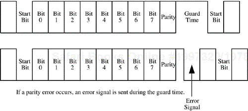
Those well versed in communication protocols might see this error detection and recovery mechanism as being somewhat prone to less-than-perfect behavior. This indeed tends to be the case in actual practice. For most readers, however, the channel tends to be very good or very bad. If it's very good, then this error detection and recovery mechanism is seldom used; if it's very bad, then the error detection and recovery mechanism is likely to fail at some point. This leads to the transmitting and receiving sides of the channel getting out of synchronization. If this situation is detected by the card, it usually will be programmed to go mute and quit responding to commands from the reader. At this point, or if the reader detects the ambiguous state first, the reader will issue a reset signal to the card that forces the communication protocol to be brought up from scratch.
The TPDU for the T=0 protocol comprises two distinct data structures: one that is sent from the reader to the card (as a command) and one that is sent from the card to the reader (as a response). The command header (sent from the reader to the card) includes five fields:
CLA. A 1-byte field that establishes a collection of instructions; this is sometimes referred to as the class designation of the command set.
INS. A 1-byte field that specifies a specific instruction (to the card) from within the set of instructions defined within the CLA designation; this is sometimes referred to as the instruction designation within the class of commands.
P1. A 1-byte field used to specify the addressing used by the [CLA, INS] instruction.
P2. A 1-byte field also used to specify the addressing used by the [CLA, INS] instruction.
P3. A 1-byte field used to specify the number of data bytes transferred either to the card or from the card as part of the [CLA, INS] instruction execution.
The procedure bytes, which are sent from the card to the reader, used to respond to the reader's command, include three or four fields:
ACK. A 1-byte field that indicates reception (by the card) of the [CLA, INS] command.
NULL. A 1-byte field used by the card to essentially do flow control on the I/O channel; it sends the message from the card to the reader that the card is still working on the command and signals the reader not to send another command just yet.
SW1. A 1-byte field used by the card to send a status response back to the reader regarding the current command.
SW2. A 1-byte field that may be included in the procedure bytes, depending on the specific command being executed. If included, it also conveys a status response back to the reader.
As indicated previously, the T=0 protocol tends to mix elements of application-level protocols with elements of link-level protocols. The definition of the CLA byte is one such case in point. Each value of CLA defines an application-specific set of instructions; the individual instructions have a unique INS value. The first set of application-oriented commands is found in ISO/IEC 7816-4; the specific command sets are aimed at manipulation of a file system on a card and at accessing “security” commands on a card. Other standards documents define additional sets of commands (that is, additional values of the CLA byte). Some of these are listed in Table 3.9. The specific instructions found in these classes will be reviewed a little later in this chapter.
Table 3.9. CLA Instruction Set Definitions
CLA Byte | Instruction set |
|---|---|
0X | ISO/IEC 7816-4 instructions (files and security) |
10 to 7F | Reserved for future use |
8X or 9X | ISO/IEC 7816-4 instructions |
AX | Application- and/or vendor-specific instructions |
B0 to CF | ISO/IEC 7816-4 instructions |
D0 to FE | Application- and/or vendor-specific instructions |
FF | Reserved for protocol type selection |
Within a given CLA value (that is, within a class of instructions identified by a common value of CLA), the INS byte is used to identify a specific instruction. As indicated in Table 3.9, several different standards identify collections of instructions. The ISO/IEC 7816-4 standard identifies a number of instructions used to access an on-card file system and security functions that serve to limit access to the file system and to the card in general. This instruction set is listed in Table 3.10.
Table 3.10. ISO/IEC 7816-4 INS Codes
INS Value | Command Name |
|---|---|
0E | Erase Binary |
20 | Verify |
70 | Manage Channel |
82 | External Authenticate |
84 | Get Challenge |
88 | Internal Authenticate |
A4 | Select File |
B0 | Read Binary |
B2 | Read Record(s) |
C0 | Get Response |
C2 | Envelope |
CA | Get Data |
D0 | Write Binary |
D2 | Write Record |
D6 | Update Binary |
DA | Put Data |
DC | Update Record |
E2 | Append Record |
Note
At this point, a portion of the discussion related to how EEPROM memory is programmed should be reiterated. In early microprocessor chips that included EEPROM memory, a separate power source (VPP) was needed to program (i.e., erase and write) EEPROM memory. ICCs used in current smart cards are able to derive “programming power” for NVM from the VCC power, so any significant discussion regarding VPP has been omitted. When the ISO/IEC 7816 Standard was adopted, however, the proper manipulation of the VPP power was necessary and was subsequently embedded rather deeply into the T=0 protocol. Specifically, the manner in which the INS byte is defined and in which the ACK procedure byte is returned are, in effect, the control mechanisms for VPP. Suffice it to say that all INS values must be even because the low-order bit allows control over VPP to be exercised. Further, in the absence of any manipulation of VPP, the ACK procedure byte is always returned as an exact copy of the INS byte in the command TPDU to which the procedure bytes form a response.
There are additional constraints on the values the INS byte can take; specifically, the high-order half-byte cannot have the value of either 6 or 9. In both cases, the restricted values are related to control mechanisms used to manipulate the VPP power source. The reader is referred to the ISO/IEC 7816-4 standard if further discussion is desired.
Note
ISO/IEC standards are available from:ISO/IEC Copyright OfficeCase Postale 56CH-1211 Geneve 20Switzerland
Copies of international standards, catalogs, and handbooks (ISO and IEC), as well as all foreign standards from ISO member body countries (DIN, JISC, BSI, AFNOR, and so on), are available in the United States from:
ANSI11 West 42nd StreetNew York, NY 10036212-642-4900 (voice)212-302-1286 (fax)
The command header parameters P1 and P2, although defined at what should be the link-protocol level, are actually dependent (for their specific definition) on the actual instruction specified; that is, their definition is actually dependent on application protocol information. P1 and P2 provide control or addressing parameters for the various application-specific instructions. For example, one application instruction, which is examined later, involves the selection of a specific file within the card's file system; selecting a file then allows subsequent operations such as reading or writing to be performed on the selected file. For this specific instruction, the parameter P1 is used to control how the file will be referred to in the select operation (i.e., Will it be referred to by an identifier, by name, or by path?). When the Select File instruction is reviewed, the strict definitions of those terms will be considered; however, for the reader familiar with general file systems on various computer systems, the meanings can be readily inferred. For the Select File instruction, the parameter P2 offers further refinement of just which file is to be selected.
The command header parameter P3 also is an application-level parameter. For many instructions, the P3 parameter can take on rather complex connotations (e.g., multiple parameters are defined within it). When the TPDU structure is examined, it is found that P3 generally defines the number n of data bytes that are to be transmitted during the execution of the INS-specified instruction. The direction of movement of these bytes is dependent on the instruction. The convention of movement of data is card-centric; that is, outgoing means data moving from the card to the reader, while incoming means data moving from the reader to the card. A value of P3=0 for an instruction specifying an outgoing data transfer means that 256 bytes of data will be transferred from the card to the reader.
Each time a command TPDU is sent from the reader to the card, a response TPDU is returned from the card to the reader. This response TPDU is made up of a number of procedure bytes. The first byte of this TPDU is an ACK byte. This byte is simply a repeat of the INS byte from the command TPDU to which this response is made. The second byte is the NULL byte. This byte is simply a way for the card to mark time while it processes the indicated command. While it is processing, the reader side of the channel is waiting for the response TPDU. If the response does not arrive within a specified timeout period, the reader may start an RST sequence to reinitialize the protocol between the reader and the card. This is prevented if at least a NULL response is received by the reader from the card.
SW1 is a status byte from the card to tell the reader the result of the requested instruction. The allowed values for SW1 are actually defined as part of the application protocol. For certain instructions, the card may have data bytes to be returned to the reader. In this case, a second status byte labeled SW2 is returned to the reader. This acts as a trigger for the reader to now execute another command called a GetResponse command, which will actually return the data bytes generated by execution of the previous command.
As you can see, the T=0 protocol is a relatively optimized protocol for moving commands and responses between the card and reader. It tends to blur the distinctions between the application-layer protocol and the link-layer protocol, with many of its constituent elements actually being defined within the application-layer protocol.
The T=1 protocol is a block-oriented protocol. This means that a well-defined collection of information (i.e., a block) is moved as a single unit between the reader and the card. Embedded within this block structure may be an APDU defined for a specific application. This facility is a good illustration that the T=1 protocol provides excellent layering between the link protocol layer and the application protocol layer. Moving information in a block, however, requires that the block be transferred (between the reader and the card) error free, or else the protocol can rather easily get lost. The error detection and correction, then, is a significantly more complex operation than was the case with the T=0 protocol.
Error detection in the T=1 protocol is done by using either a longitudinal redundancy character (LRC), which is essentially a slightly more complex form of parity checking than was done in the T=0 protocol, or by using a cyclic redundancy check (CRC) character, which (unlike any parity check) is guaranteed to detect any single-bit errors in a transmitted block. The specific CRC algorithm used is defined in detail in the ISO 3309 Standard. When an error is detected within a block by the received end of the channel, it signals the transmitting end to repeat sending the block received in error.
The T=1 protocol makes use of three different types of blocks, as illustrated in Figure 3.10. Each has the same structure, but serves a different purpose:
Information block. This block is used to convey information between application software in the card and application software on the reader side of the channel.
Receive ready block. This block is used to convey either positive or negative acknowledgments from one end of the channel to the other. A positive acknowledgment indicates that a block was correctly received while a negative acknowledgment indicates that an error was detected (via checking the LRC or CRC) in the received block.
Supervisory block. This block is used to convey control information between the card and the reader.

Each T=1 block comprises three fields:
Prologue field. A mandatory field in the block that is 3 bytes in length. It includes the following three elements:
NAD. Node address.
PCB. Protocol control byte.
LEN. Length.
Information field. An optional field in the block, which may be up to 254 bytes in length.
Epilogue field. A mandatory field in the block, which is either 1 or 2 bytes in length.
The NAD element is used to identify the addresses of the source of the block and the intended destination for the block. This addressing facility is of greatest use when the T=1 protocol is being used to support multiple logical connections between the card and multiple application connection points on the reader side of the channel. When used, the NAD contains two subfields:
SAD. Source address is indicated by the low-order three bits of the NAD byte.
DAD. Destination address is indicated by bits five through seven of the NAD byte.
In situations where multiple logical channels are not being used, the NAD byte is set to all zeros. The two other bits of the NAD byte, those not used for the SAD or the DAD, are used to convey information related to controlling the VPP (EEPROM programming power).
The PCB element is used to indicate the type of block (i.e., either an information, a receive ready, or a supervisory block). The two high-order (most significant) bits of the PCB byte are used to denote the various types:
A high-order bit set to 0 indicates an information block.
The two high-order bits set to 1 indicate a supervisory block.
The high-order bit set to 1 and the next bit set to 0 indicate a receive ready block.
T=1 is a relatively complex protocol. As a block-oriented protocol, error detection and retransmission occur at a block level. Much of the complexity comes from establishing the correct ordering of message blocks as errors occur and are corrected for. For purposes of this discussion, the protocol is viewed as was the T=0 protocol (i.e., as a reliable channel for moving APDUs between application software elements on the card and on the reader side of the communication channel). The other protocols that can be defined through the ATR and/or PTS sequence (i.e., T=2, …, T=14, T=15) serve this same purpose.
The ISO/IEC 7816-4 standard moves from the realm of defining base system functionality for smart cards into the realm of functionality directly useful to application software found on the smart card. Two areas of functionality are addressed:
First, a file system is defined with a completely specified hierarchical structure. A set of functions are defined; these functions comprise an API through which application software on the reader side of the channel can access the files and information in those files within this file system.
Second, a series of security functions are defined, which can be used to limit access to application software on the card or to files and information in those files within the card's file system.
This application software makes use of a protocol to exchange control and information between the reader and the card. This protocol is based on a block structure called an APDU. These APDUs are exchanged by making use of the T=0 and T=1 link-layer protocols. A software component on the card interprets these APDUs and performs the specified operation; this architecture is illustrated in Figure 3.11.

The APDU structure defined in ISO 7816-4 is very similar to the TPDU structure defined in ISO 7816-3 for the T=0 protocol. When the APDU structure is transported by the T=0 protocol, the elements of the APDU directly overlay the elements of the TPDU; hence, the comments earlier about the lack of effective protocol layering with the T=0 protocol.
An ISO 7816-4 APDU is
Link-level protocol independent
Defined at the application level
An instruction APDU is a message structure that carries a command or instruction (and perhaps data) from the reader to the card. A response APDU is a message structure that carries a response (and perhaps data) from the card back to the reader. We'll examine the ISO 7816-4 command set in some detail in Chapter 4.
Throughout their history, smart cards have been subjected to a stringent requirement that their development and deployment be controlled through standards; standards which come from a variety of sources. Standards defined through international standards bodies establish much of the framework for classical smart card infrastructures. The physical and electrical characteristics of the card and its embedded ICC along with the operational paradigm and essential security characteristics are so defined.
In addition, many specifications for card operational characteristics are defined through consortia. In some instances, such specifications have evolved into international standards. Finally, many characteristics of the latest generation cards are subject to definition and protection as intellectual property. All of these mechanisms, taken together, establish a very well-defined framework into which smart cards must fit. While this certainly establishes a well-regulated marketplace for vendors and customers alike, it does make for a tough environment for rapid or revolutionary developments to occur.
The initial startup sequence for smart cards is defined through well-established standards. In this chapter, we have reviewed this procedure and had a brief overview of the base-level communication protocols used between cards and terminals. In the following chapter, we will move “up” the protocol stack to look at the application-level mechanisms used to communicate between cards and terminals.