Logic circuits
Whether we are reading the time on a digital watch, dialling a call on a mobile phone, listening to a compact disc, using a Smartcard, or sending an e-mail, we are using logic circuits. More and more of the equipment we use at home and at work depend on electronic logic. Logic is the science of reasoning, and we use its electronic equivalent as the basis for a whole host of so-called ‘intelligent’ devices.
The form of logic most suitable for implementing electronically is binary logic. In binary logic, we deal with only two states. A statement is true or it is untrue: there are no half-truths. A digit is 1 or 0: there are no fractions or other values. A transistor is either fully on (saturated) or fully off: it switches rapidly from one state to the other, spending a negligible time in the intermediate states. A voltage is either high or low: intermediate values have no meaning.
The on-off, high-low characteristics of binary logic mean that we can design electronic circuits that can model logical statements with absolute accuracy. We need to be concerned with only two voltage levels, not with all the possible levels that exist in (for example) audio circuits. Nowadays, even audio circuits are mainly digital but, at least, in their input and output sections, we have a continuous range of voltage levels.
Let us see how a logical situation may be modelled electronically. Take as an example the floodlight illustrated in the title photograph of Chapter 12. A floodlamp beside a garage is to be switched on whenever a car or a person approaches the garage, but this is to happen only at night. There is no point in turning on the floodlight during the day. There are two sensors. One of these, perhaps based on a light-dependent resistor responds to light level. It can be arranged, possibly by using a Schmitt trigger circuit, that the output voltage of the sensor circuit is low (close to 0 V) when it is daylight and high (close to the supply voltage) at night. The other sensor is a pyroelectric sensor; it responds to the heat radiating from the car or from the body of the approaching person. Its circuit is arranged to give a high output when it is triggered.
The logic required is simple. If the LDR detects night AND the pyroelectric device detects heat, the floodlight comes on. The AND in this sentence is an example of a logical operator. It links the two conditions under which the floodlamp is to be turned on. It tells us that we must have one condition (night) AND the other condition (heat detected) in order to turn on the floodlamp. Putting it another way, we have three statements:
B = a car is approaching
Z = the floodlamp is on
Any of these statements may be true or not true, but the truth or otherwise of Z depends on the truth of A and B. The logic of the lighting control, expressed in short form is:
IF A is true AND B is true THEN Z is true
or even shorter
The ‘IF … THEN …’ format appears often in binary logic.
Inverse statements
Each of the statements above can be paired with an ‘opposite’ statement so that, if the statement is not true, its ‘opposite’ or inverse is true. The inverse is represented by the same letter as the_original statement, but with a bar over it. For example, if A = ‘it is night’, then Ā = ‘it is not night’.
In most contexts, including the example above, we accept that ‘it is not night’ means the same as ‘it is day’. But, at dawn and dusk, people could be justified in stating that it is not night, yet it is not day either. So, ‘it is day’ is not a strict inverse of ‘it is night’. The only exact inverse is ‘it is not night’. This difficulty does not arise with Z = ‘the floodlamp is on’, which has the inverses ![]() = ‘the floodlamp is not on’, and
= ‘the floodlamp is not on’, and ![]() = ‘the floodlamp is off’ because ‘off’ and ‘on’ are exclusive opposites. Because we have additional knowledge about floodlamp systems, we are able to use the other inverse. However, if in doubt, always make the inverse by inserting ‘not’.
= ‘the floodlamp is off’ because ‘off’ and ‘on’ are exclusive opposites. Because we have additional knowledge about floodlamp systems, we are able to use the other inverse. However, if in doubt, always make the inverse by inserting ‘not’.
Logical operators
There are three basic logical operators that are used in ‘IF … THEN … ‘ statements:
NOT: IF A is true, THEN ![]() is NOT true. Since all statements must be true or not true, this implies that if A is NOT true THEN
is NOT true. Since all statements must be true or not true, this implies that if A is NOT true THEN ![]() is true.
is true.
Example IF it is night THEN it is NOT daytime (assuming we ignore dawn and dusk).
AND: IF A is true AND B is true, THEN Z is true. Otherwise Z is not true (false).
Example IF it is night AND a car approaches, THEN the floodlamp comes on.
OR: IF A is true OR B is true, THEN Z is true. Otherwise Z is not true (false).
Example At night, if a person approaches OR a car approaches, THEN the floodlamp comes on.
The full operation of the floodlamp controller depends on the AND and OR operators. We shall shortly look at ways in which these operations can be performed electronically.
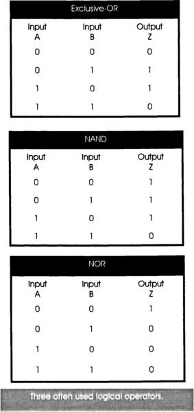
Truth tables
The action of logical operators can be represented by truth tables in which ‘1’ represents ‘true’ and ‘0’ represents ‘not true’, or ‘false’. Alternatively, we could use the letters ‘T’ and ‘F’. We list the ‘IF’ conditions A,B under ‘Input’ and the ‘THEN’ consequence Z under ‘Output’. On the opposite page are the three tables that cover the logical operators we have just discussed.
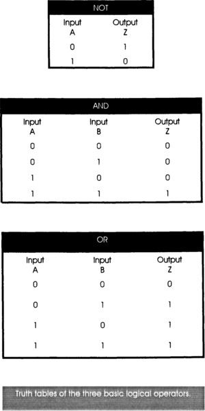
Except for the NOT operator, logical statements can be extended to include more than two conditions. For example, IF A is true AND B is true AND C is true AND D is true, THEN Z is true. Otherwise, Z is false.
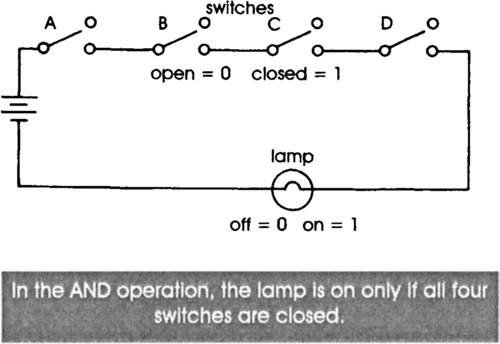
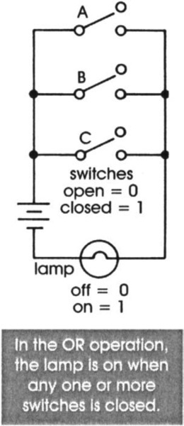
It is a simple matter to perform the basic operations using ordinary manually operated switches, with a lamp to indicate the logical outcome. This is how we perform the AND operation on A,B,C and D.
For calculators, clocks and computers we need full electronic switching at high speed, combined with reliable action, freedom from interference from occasional voltage fluctuations and ‘spikes’, and outputs that are firmly high or low. Logic circuits that meet these specifications are made in integrated form and we consider some of these in the next section.
All logical situations can be expressed in terms of NOT, AND and OR, but there are three other operators that are often used to simplify the statements:
EXCLUSIVE-OR, sometimes known as EX-OR: If A OR B but NOT BOTH are true, then Z is true.
NAND: This is the AND operation followed by NOT.
NOR: This is OR followed by NOT.
All logical operations can be performed using just the NAND operator or the NOR operator. Statements using only NAND or NOR may be longer and more difficult to understand that those which use the simpler AND, OR, and NOT operators, but there is sometimes a practical advantage. It can be more economical when building a logical circuit to employ only one type of operator and the wiring may be simpler.
Transistor-transistor logic
Although transistor-transistor logic (or TTL, as it is more usually called) has been largely superseded by other forms with superior performance, it is TTL which was the dominant type in the expanding days of the seventies and early eighties. Many of the logic ICs today are simply upgraded versions of the original TTL, performing the same functions and having the same pin connections.
The circuit element that performs a single logical operation is known as a gate. The circuit has an unfamiliar component which is a transistor with two emitters. If both emitters are connected to the positive supply voltage (logical high, equivalent to A AND B) the transistor does not conduct. The effect of this on the remainder of the circuit is to make the output Z go low. The transistor is turned on when either one or both emitters are connected to 0 V (logical low), any combination of inputs making the output go high
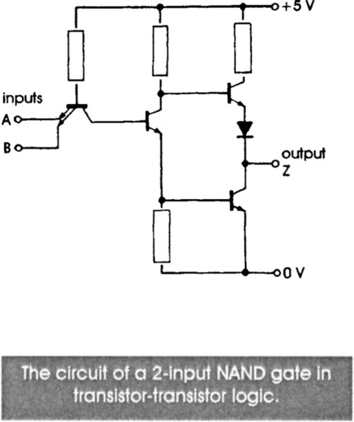
The behaviour of the circuit mirrors the action of the NAND operator. One might wonder why it requires such a complicated circuit to perform this operation. One function of the other components is to ensure fast action. The other function is to ensure that the voltages at high and low levels are clearly distinguished, with no half-way states possible.
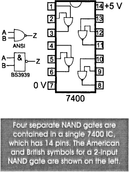
Even though the circuits of the descendants of TTL are appreciably more complicated, they are still simple enough from the point of view of integration, and they occupy little space on the silicon chip. Four independent gates are fabricated on one chip in a 14-pin package.
TTL and its derivatives comprises a large family of several hundred different ICs. Some of these consist of relatively simple gates but others employ MSI and LSI (p. 164) to build complex counters, registers and logical arrays on a single chip. The chief advantage of TTL is its high speed, making it suitable for use in computers. It requires a supply voltage between 4.75 V and 5.25 V so a regulated supply is virtually essential. Electrical noise such as ‘spikes’ on the supply lines are liable to upset its operation. The power supply needs to be well filtered to remove this interference.
Its main disadvantage is that it requires fairly large currents to operate it. Even a relatively small system consisting of half-a-dozen ICs may require a supply of 1 A, which means that the use of TTL in battery-powered equipment is severely limited. This has prompted the development of versions of TTL that are less power-hungry. One of the most popular of these is low-power Schottky TTL, or LSTTL. Power requirements are reduced to about a fifth of those of standard TTL by increasing the values of the resistors in the circuits. The name ‘Schottky’ refers to an element in the circuit known as a Schottky clamp. The function of this is to prevent transistors that are turned on from being fully saturated. Saturated transistors take longer to switch off than transistors that are not saturated because it is first necessary to remove excess charge carriers from the base region of the transistor. The Schottky clamp forward-biases the transistor by only a few tenths of a volt so that it turns off quickly. The LS series is not much faster than standard TTL, but the newer Advanced low-power Schottky version is twice as fast and uses about one-twentieth of the power of standard TTL.
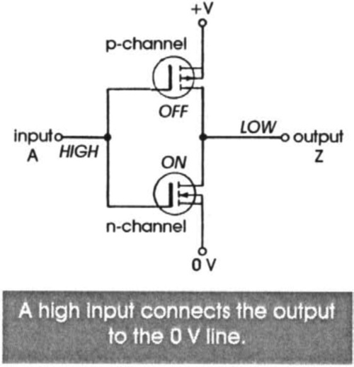
CMOS logic
Although standard CMOS logic (the best known is the 4000 series) operates about 10 times more slowly than TTL and its variants, this is no disadvantage in many applications. Its chief advantage is that it has very low power consumption, making it ideal for battery-powered portable equipment. When gates are not actually changing state they require practically no current at all, so quiescent power requirements are very low indeed. CMOS operates on any supply voltage between 3 V and 15 V. A regulated power supply is not required. An LSTTL output can drive only about five LSTTL inputs and similar limitations apply to the other TTL versions. By contrast, a CMOS output can drive a practically unlimited number of CMOS inputs. This makes circuit design much simpler.
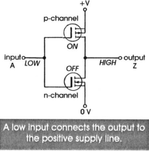
The ‘C’ in the acronym CMOS stands for ‘complementary’ and the figure explains what this means. The gate consists of two MOSFETs of complementary type, n-channel and p-channel Given a high input, the p-channel transistor is turned off and the n-channel input is turned on. This more or less short-circuits the output to the 0 V rail, giving a low output. Conversely, a low input turns on the p-channel transistor and turns off the n-channel transistor, short-circuiting the output to the positive supply rail. The action corresponds to the logical NOT operator.
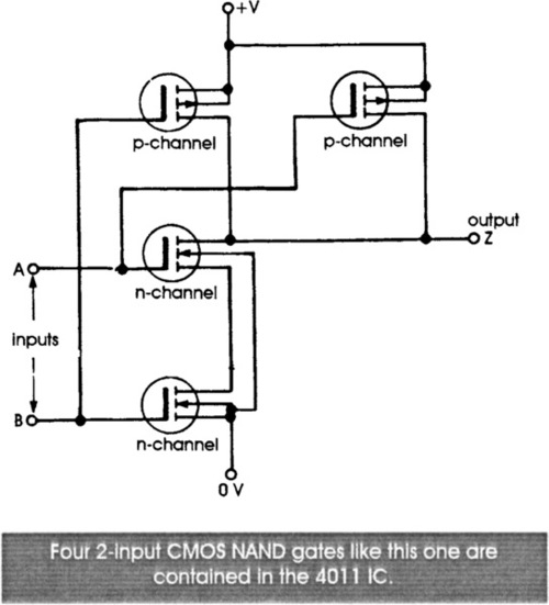
The NAND gate illustrated on the opposite page operates in a similar fashion. The output is connected to the 0 V line only if both inputs are high, switching on both n-channel transistors. Other combinations of inputs connect the output to the positive supply line.
Because CMOS works by short-circuiting the output terminal to one or other of the power rails, the output voltage is very close to one or other of the supply rails. There is a clear distinction between the high output level and the low level. This is why CMOS is relatively unaffected by noise and ‘spikes’ on its supply lines.
The diagram also illustrates the fact that the CMOS gate requires few components compared with a TTL gate. Thousands of gates can be accommodated on a single chip so that CMOS is ideal for LSI and VLSI, Consequently the CMOS range of logic circuits includes devices such as 16-stage counters and 64-stage shift registers that are not available in TTL.
CMOS transistors, like all MOS transistors, have very high input impedance, so they require virtually no current to alter the potential of the gate. We can understand why the current requirements of CMOS are exceedingly small, and why current is required only when the input to a gate is being changed.
Transmission gates
In this type of gate, the n-channel and p-channel transistors are both switched on by a high control input and are both switched off by a low control input.
The circuit acts as an electronically-controlled switch and can be controlled by the output from another CMOS gate. When the transistors are off, only a minute current of a few nanoamps can flow between the terminal on the left to the terminal on the right. When the transistors are on, the resistance between input and output terminals is only about 80 Ω, the gate acting as a low-value resistor.
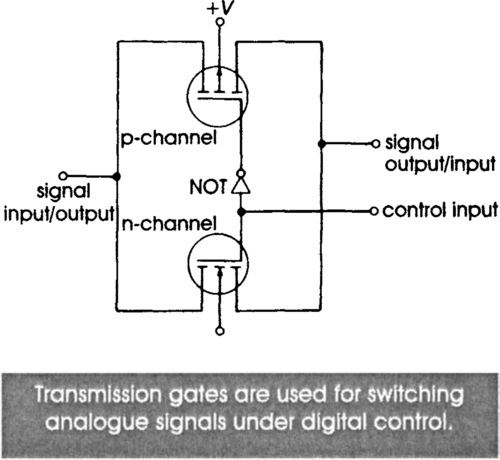
When the gate is switched on, current can flow freely through it in either direction, which is why we refer to its terminals as input/output terminals. Transmission gates are used for switching analogue signals (for example, audio signals) may range in size between 0 V and the supply voltage.
The gate shown above acts as a single-pole on-off switch. Other CMOS transmission gate ICs have two or more transmission gates with common control lines. These make it possible to implement other switching actions, such as changeover switches, double-pole double-throw switches, and 1 -of-4 (or more) selector switches, all under logical control.
Other logic
Among the other logic families, each with its own characteristics and special applications, is high-threshold logic (HTL) or high noise immunity logic (HNIL). The gap between the low and high logic levels is particularly large, which makes the series suited to industrial environments. There, electrical noise often makes it impractical to use TTL or CMOS.
Emitter-coupled logic (ECL) is designed for very high-speed operation; as with Schottky devices, the transistors are prevented from becoming completely saturated, but in this family this is achieved by having the logical low and high levels close together. This makes ECL liable to noise interference. Also, it requires more power, as the transistors are bipolar types and are always switched on. The HC family is very popular. It has CMOS-based gates but runs at high speed. It combines the best features of TTL and CMOS. Most of the standard TTL devices are available as HC types, and there are HCT devices intended for interfacing directly with TTL.
Logic and numbers
Electronic logic involves only two states; on and off, high and low, 1 and 0. But the numbers we use in everyday life rely on having 10 different symbols (0 to 9) to express them. To convert these directly to electronic form would mean having 10 input and output levels. Although it is possible to do this, the circuitry required is much more complicated than that used for logic gates. We throw away the advantages of high-speed operation, reliability, noise-immunity, and the ease of implementing the circuits in MSI and LSI. It is much more sense to abandon the decimal system and replace it with a number system that has only two values, 0 and 1. This is known as the binary system.
In the decimal system, the value of a digit is determined by its place in the number. For example, the number ‘374’ means 3 hundreds plus 7 tens plus 4 units. In the number ‘6267’, the first ‘6’ means 6 thousands, but the second ‘6’ means 6 tens. Value depends on position. As we go from right to left, the position value increases by 10 times.
The binary system works on the same principle but in twos instead of tens. The position values from right to left are units, twos, four, eights, sixteens and so on, doubling up each time we shift one place to the left. So the binary number 110 is the equivalent in decimal of 1 four plus 1 two plus no units, totalling 4 + 2 + 0 = 6. Similarly, the binary number 1010 is the equivalent of 1 eight plus no fours plus 1 two plus no units = 8 + 0 + 2 + 0 = 10.
Mathematics is a logical process so it is not surprising that we are able to use logic circuits to perform mathematical operations. As a simple illustration, consider the addition of two single-digit binary numbers, either of which may be 0 or 1. The results of all possible additions with these two numbers are:
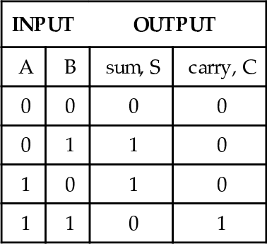
The addition in the last line of the table would normally be written with the carry digit on the left: 1 + 1 = 10. In decimal, this is the equivalent of 2 + 2 = 4 as can be seen from the table on page 215.
If we compare the value S in the sum column with the output values of the truth tables on page 188 we find that S is the equivalent of Z for an EXCLUSIVE-OR gate.
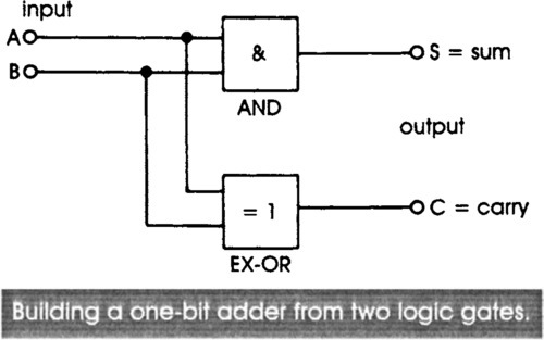
Similarly, matching the value of C in the carry column, we find that this is the same as Z for an AND gate. Given an EXCLUSIVE-OR gate and an AND gate, we can use them to add two single-digit binary numbers. Addition of binary numbers with more than a single digit is naturally more complicated, as we have to allow for adding in the carry digits at each stage, but it is easily done with suitably connected logic gates. The addition circuit is usually presented as an MSI device. Other mathematical operations can also be performed by logic. For example, we can multiply two numbers together by adding the same number to itself repeatedly and counting the number of times we add it.
Programmable logic
Logic circuits can be built from a standard range of logic ICs of the kinds described above. All we need to do is to work out what gates are required and how to connect them together. Anyone who has attempted to design even a fairly simple logic circuit knows that the number of ICs required can easily mount to the twenties, thirties or even forties. These need a large circuit board, consume a large amount of power and require a complicated pattern of interconnections on the board.
For a mass-produced circuit of some complexity, such as a computer, it is possible to have specially designed LSI or VLSI circuits incorporating all the logic on one chip. But setting up production of a special IC is expensive and unlikely to be economic except for very large runs. Also, any change or improvement in the design requires the masks to be scrapped and re-designed. With programmable logic we use ICs that are produced in a few standard types, and so are inexpensive, but can be programmed to perform any of a wide range of logical operations.
One of the simplest forms of programmable logic IC is programmable read-only memory (PROM). These are normally used to store computer programs in a permanent form: for example, the system program that a computer uses when it is first switched on, to get it running. As an example, consider the simple PROM shown below, which has fewer inputs and outputs than usual, to make the diagram simpler.
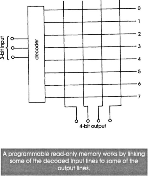
This has three inputs and four outputs. The inputs go to a three-line to eight-line decoder. For each of the eight possible combinations of states of the inputs (000 to 111), one of the eight lines goes high.
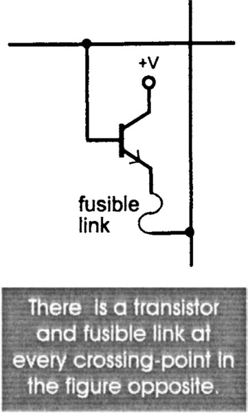
There is a link between each of these lines and the four outputs, the link consisting of a transistor and a fuse. When the device is programmed, other circuits not shown in the figure allow us to decide which fuses are to be intentionally blown and which are left intact. This is what we mean by saying that the device is programmable. Suppose the input is 110, so that line 6 is made high. If all the fuses are present, base current is supplied to all transistors on that line and all four output lines go high; the output is 1111. But some of the fuses may have been blown when the device was programmed. If any fuse is blown the corresponding output stays low.
Depending on which fuses are blown, the output corresponding to an input 110 can be any one of the sixteen 4-bit binary numbers from 0000 (all blown) to 1111 (none blown). Once a fuse has been blown it can not be repaired, so the device is programmed once and for all. After that, it is possible only to read the data stored in it, but not to change it, which is why it is called a read-only memory.
Used as a memory, the device is programmed with data which might be a table of information or might be the steps of a program in code. According to the 3-bit input (or address), we obtain an output corresponding to the stored data. The use of the PROM as a logic array is similar, as shown by the following example. An automatic lamp-switching system for a shop has three inputs: a passive infra-red detector in the store-room, a light sensor to detect if it is day or night, and a weekly timer to register if the day is Sunday or not. The output goes to four sets of lamps: the shop, an illuminated display in the shop, the store room, and the car park. The lamps are to be switched on as follows:
In the shop: every night, every day of the week.
The display: during day-time, every day, except Sunday.
In the store room: all the time, except day-time on Sunday.
In the car park: if a car is detected at night, except Sunday night.
The truth tables for these requirements is:
| INPUT | OUTPUT | |||||
| I-R (1 = car) | Day/Night (1 = night) | Day (1 = Sunday) | Shop lamps (1 = on) | Display lamps (1 = on) | Store lamps (1 = on) | Car park (l=on) |
| 0 | 0 | 0 | 0 | 1 | 1 | 0 |
| 0 | 0 | 1 | 0 | 0 | 0 | 0 |
| 0 | 1 | 0 | 1 | 0 | 1 | 0 |
| 0 | 1 | 1 | 1 | 0 | 1 | 0 |
| 1 | 0 | 0 | 0 | 1 | 1 | 0 |
| 1 | 0 | 1 | 0 | 0 | 0 | 0 |
| 1 | 1 | 0 | 1 | 0 | 1 | L |
| 1 | 1 | 1 | 1 | 0 | 1 | 0 |
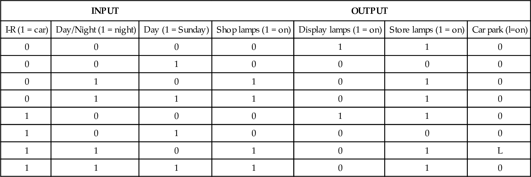
The table has eight rows, covering all possible combinations of inputs. The outputs could be obtained by using a number of NAND and NOR gates, but blowing the fuses of a PROM to correspond with the l’s in the output columns of the truth table achieves the same effect with just a single IC and there is no need for connections between gates.
Sequential logic
The logic we have considered so far is combinatorial logic. We set up a number of fixed inputs to the circuit and the output takes a given value, depending upon the truth table or tables of the circuit. Given a certain combination of inputs, the circuit always behaves in the same way. In sequential logic, the behaviour of the circuit is partly or wholly dependent on what has been happening to it previously. A sequential circuit built with transistors is the flip-flop (or bistable) circuit shown on page 170. We give it a low input by connecting input A briefly to ground. What happens as a result of this input depends upon what state the circuit is in.
If output A is high, nothing happens. If output A is low, it changes to high. The behaviour of the flip-flop goes through a sequence of events. This is just a simple example of a sequential circuit but, from a simple flip-flop, we can build up more complicated circuits such as counters. The four outputs from a counter made from four connected flip-flops take one step through the sequence 0000, 0001, 0010, 0011, … , 1111 each time the input to the first flip-flop is grounded. It counts from 0000 to 1111 in binary, that is from 0 to 15 in decimal. Sequential logic is important for the control of equipment such as an automatic drilling machine or a robot which has to perform a sequence of different tasks.
Logic circuits and the outside world
Logic circuits operate on electronically-represented facts but a logic circuit on its own cannot operate on any facts unless it has been told what they are. At the other end of the process, the circuit needs to be able to communicate the results of its operations to the user.
One of the most obvious and simplest ways of giving facts to a logic circuit is to open or close a switch. It might be a micro-switch attached to a door. When the door is open the switch is open; when the door is shut the switch is closed. The switch tells the logic circuit about the state of the door. But even such a simple arrangement has its problems. One of the major ones is contact bounce. It happens when we operate any switch, such as a key on a keyboard. As the key is pressed and the contacts come together, they do not necessarily stay together. They may make and break several times as the switch closes, closing together finally when the switch has reached the end of its travel. Contact bouncing may take as long as 20 ms.
This ‘off-on-off-on-off-on-off-on’ nature of a switch is unimportant when, for example, we are switching on a room lamp. The response of the lamp is slow, since it takes an appreciable time to heat up the filament to the temperature at which it begins to emit light. By the time it is heated the contact bouncing is over. The lamp does not appear to flash on and off. But logic circuits are fast, operating in microseconds or even nanoseconds. They have no difficulty in responding to every off-on change. If a logic circuit is being used to count how many times we press a key it counts once for every off-on change. We press the key once, but the counter may register 4 or more off-on changes.
The solution to this problem is to de-bounce the switch or key. The figure overleaf shows a debouncing circuit using a flip-flop (p. 170). Here the flip-flop is a logic IC, not made from discrete components, but its action is the same.
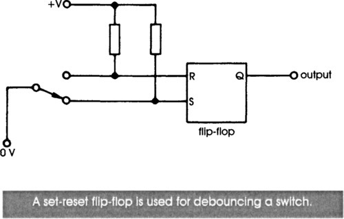
The two inputs, corresponding to inputs A and B on p. 170 are known as the ‘set’(S) and ‘reset’ (R) inputs. When not connected to the 0 V line by the switch they are held high by the resistors. Connecting S to 0 V sets the flip-flop. Its output Q goes high. Connecting S to 0 V again has no effect, for the flip-flop is already set. Its output can be changed only by connecting R to 0 V, which resets the flip-flop, making Q go low.
In the figure above, the switch is connecting S to 0 V so the output is high. As we move the switch to its other position, contact bounce will cause makes and breaks between S and the 0 V line, but this has no effect on the flip-flop. However, the first time that the switch connects R to the 0 V line, the flip-flop changes state and its output goes high. Having done so, it is completely unaffected by any subsequent makes and breaks between R and 0 V.
One of the most important differences between a logic circuit and the outside world is the way in which quantities are represented. In the real world, temperature is a quantity which changes smoothly as an object is warmed or cooled. On a mercury thermometer we can see the end of the column moving smoothly up or down the tube. The thermometer scale may be marked in degrees but we can estimate fractions of a degree quite easily. The same applies when we use a thermistor. Temperature changes smoothly and so does the resistance of the thermistor. If the thermistor circuit represents changes in resistance as changes in voltage at its output, we find that the voltage changes smoothly too.
The way the voltage changes mirrors the way the temperature is changing. The rate and extent of the change in voltage corresponds to the rate and change of the temperature. We say that the voltage is an analogue of the temperature. In the same way, a microphone is sensitive to pressure changes in the air caused by sound waves. It generates an alternating voltage which we can amplify. The waveform of the amplifier output is an analogue of the waveform of the original sound.
By contrast there are no smoothly varying quantities in a logic circuit. Voltages change abruptly from 0 to 1 and 1 to 0, and in-between states are not recognized. A value is represented as a binary number which exists in the circuit as a series of highs and lows, representing the digits of the binary number. The value is represented in digital form. Informing a logical circuit about quantities in the outside world first involves converting it to an electrical analogue, usually a voltage, and then converting the voltage into digital form. Converting into an analogue is done by using a sensor such as a thermistor or microphone with a suitable circuit such as an amplifier to produce an analogue voltage. Converting this voltage into digital form is done by using an analogue-to-digital converter, or ADC.
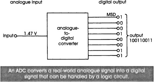
The details of how an ADC works are too complex to go into here. An ADC is usually an integrated circuit which has a single input to which the analogue voltage is fed. It has a number of logic outputs, often eight or twelve, which may be high or low. The outputs produce an 8-bit or 12-bit binary number, its value depending on the voltage fed to the IC. If there are 8 bits, the output ranges from 0000 0000 to 1111 1111. In decimal this is from 0 to 255. There are 255 steps from the bottom to the top of the range.
For convenience (and also to simplify this explanation) we may set the analogue input to range over the values 0 V to 2.55 V. 2.55 V divided into 255 steps gives 0.01 V per step. If the input increases by 0.01 V, the output increases by 1. If the input is 1.47 V, the output is 147 in decimal, represented by 10010011 in binary.
With an 8-bit ADC as described above, while the input may vary smoothly, taking any value between 0 and 2.55 V, the output is allowed to take only 256 different values in steps of 0.01 V. The resolution of such an ADC is 0.1 V. This may be sufficiently good for many applications. A 12-bit ADC gives much better resolution since there are 4096 steps in increasing from 0000 0000 0000 to 1111 1111 1111.
After a logic circuit has performed its logic and its calculations it needs to make contact with the outside world again. Logic circuits can drive indicators such as LEDs directly, as well as seven-segment LED displays and LCD displays. Through the action of a transistor, a relay or an optocoupler, they can switch lamps, motors, solenoids and various other devices on or off. Sometimes a simple on-off action is not enough. The logic circuit may be required to control the brightness of a lamp or the speed of a motor, for example. In such cases the circuit must be able to produce a variable output voltage. This is usually done by using a digital to analogue converter, or DAC. The action of the DAC is the reverse of that of the ADC. It accepts an 8-bit or 12-bit binary input from the logic circuit and produces a voltage output of equivalent value. The output voltage is then used to control the brightness of the lamp, the speed of the motor or any other variable-rate process.
An alternative technique is pulse width modulation, which can be used to control the brightness of a lamp or the speed of a motor. The output of the digital circuit is a train of pulses of varying width. The actual voltage delivered to the lamp or motor is either high or low, that is, it is a binary signal. However, if the lamp is to be bright, the pulses are long ones with no gap or only a small gap between them. A motor will run at maximum speed. If the digital circuit reduces the length of the pulses and increases the gap between them, less energy is delivered to the lamp or motor. The lamp dims and the motor runs more slowly. In all cases, the pulses are of relatively high frequency, say 1 kHz or more, so that the lamp does not flicker and the motor does not run jerkily. In practice, this technique is better than an analogue voltage for controlling motor speed. The power when on is fully on, and this makes the motor less subject to stalling at low speeds.