4
Vertical NAND Flash
4.1 Overview of 3D Vertical NAND Trends
4.1.1 3D Nonvolatile Memory Overview
There is a strong potential today for 3D nonvolatile memory to replace planar memory for 10 nm nodes and beyond [1]. One candidate for bringing in the 3D era appears to be the NAND flash memory, and its basic operational modes are expected to be similar to those in the planar device. Currently, the basic types of 3D vertical memory are the vertical channel gate-all-around (GAA) NAND flash strings, the vertical gate devices with horizontal thin-film transistor (TFT) double-gate NAND flash strings, and the earlier stacked planar NAND structures discussed in Chapter 2. Both charge-trapping (CT) and floating gate (FG) 3D devices have been investigated. Some characteristics expected with the vertical channel and vertical gate CT NAND flash devices are shown in Table 4.1 [1].
Table 4.1 Comparison of 2D and Two Early 3D NAND Flash Features.
| Dimension | 2D | 3D | 3D |
| Planar | Vertical Channel | Vertical Gate | |
| Gate Structure | Stacked | Gate-all-around | Dual-gate TFT |
| Unit Cell Size | 4F2 | 6F2 | 4F2 |
| Scaling Issue | Lithography | Film thickness | Lithography/film thickness |
| Coupling | Strong | Low | Moderate |
| Coupling Direction | Word-line + bit-line | Vertical | Bit-line + vertical |
| Based on J. Choi, K.S. Seol, (Samsung), VLSI Technology Symposium, June 2011 [1]. | |||
Various issues are expected in 3D NAND flash configurations. Program disturbs may increase in 3D as a result of the proximity of cells in the z direction, and an increase is expected in various program inhibit conditions on unselected strings as a result of increased number of pages on the same word-line. Junction capacitance is expected to be significantly reduced by thin channels, and junctionless source/drain (S/D) structures should help suppress program disturbances. The vertical channel NAND is expected to be less dependent on lithography than planar NAND because thickness of materials rather than lithography will determine the bit-line (BL) and word-line (WL) pitches. Vertical gate NAND is still somewhat dependent on lithography because WLs are patterned, but BL pitch is determined by the thickness of the channel, WL, and storage layer. Basic operations are expected to be similar to those of planar devices. Primary differences are expected to be an increase in program disturbance in the z direction, which may require different program inhibit conditions on various unselected strings. Because 3D NAND flash has reduced junction capacitance due to having thin channels and junctionless S/D, program disturbance can be suppressed. A comparison of planar and two types of 3D cell arrays is shown in Table 4.2 [1].
Table 4.2 Comparison of Planar and 3D NAND Operations.
| 2D | 3D | 3D | |
| 3D Cell Array Type | Planar | Vertical channel | Vertical gate |
| WL Direction | Horizontal | Horizontal | Vertical |
| BL Direction | Horizontal | Vertical | Horizontal |
| Program/Erase | FN | FN | FN |
| Program Disturb | Channel coupling | NOP | NOP, vertical coupling |
| Stacks for 1x nm | 1 | 16–64 | 0–32 |
| Lithography Factor | Strong | Weak | Moderate |
| Based on J. Choi, K.S. Seol, (Samsung), VLSI Technology Symposium, June 2011 [1]. | |||
4.1.2 Architectures of Various 3D NAND Flash Arrays
Several 3D NAND flash array architectures that have been studied for potential products are discussed in this chapter. These include 3D CT devices with vertical pipe channel structures (e.g., P-BiCS, VRAT, TCAT, and VSAT) and with horizontal channel and vertical gate structures (e.g., vertical gate NAND and vertical gate BE-SONOS). These architectures are discussed in this chapter along with 3D vertical channel FG structures (e.g., ESCG, S-SCG, DC-SF, and SCP).
A comparison of the vertical CT architectures was given by Macronix in May of 2010 using technology computer-aided design (TCAD) simulations [2]. The structure and critical dimensions of the vertical channel TCAT, P-BICS, and VSAT architectures are illustrated in Figure 4.1 [2]. The TCAT, P-BiCS, and VSAT each have a horizontal pitch of 3F and vertical pitch of 2F, resulting in a 6F2 cell area.

Figure 4.1 Vertical channel CT NAND flash architectures. (Based on Y.H. Hsiao et al., (Macronix), IMW, 16 May 2010 [2].)
The vertical gate NAND flash architecture with stacked horizontal channels is discussed later in this chapter, and an illustration with critical dimensions is shown in Figure 4.2 [2]. The critical cell area of the horizontal channel architecture is 2F × 2F.

Figure 4.2 Stacked horizontal channel CT architectures. (Based on Y.H. Hsiao et al., (Macronix), IMW, 16 May 2010 [2].)
In June of 2007, Toshiba discussed a cost comparison of the 3D planar NAND flash with stacked single-crystal polysilicon layers, which was discussed in Chapter 2, and the 3D vertical channel bit cost scalable (BiCS) NAND flash, which is discussed in this chapter [3]. The results of this study are shown in Figure 4.3.

Figure 4.3 Cost comparison of 3D stacked NAND and BiCS 3D NAND flash. (Based on H. Tanaka et al., (Toshiba), VLSI Technology Symposium, June 2007 [3].)
The chart in Figure 4.3 is based on the formula for relative bit cost of the two architectures, which is:
Where n is the number of stacked layers, Cc is the cost for the common part, Csl is the cost per single layer, A is the area penalty rate for a single layer, and Y is the yield loss per single layer. It appears to indicate that, when the number of layers goes above about four, the relative bit cost of the 3D single-crystal layer stack also begins to rise while the bit cost of the BiCS stack continues to fall, although at a slower rate.
4.1.3 Scaling Trends for 2D and 3D NAND Cells
Scaling directions for the NAND flash cell for 20 nm and beyond were discussed by Micron Technology and Intel in December of 2012 [4]. For the conventional wrapped floating gate (FG) cell, which has the control gate (CG) wrapped around the FG, to continue scaling below 20 nm, the aspect ratio would become greater than 10 in both the WL and BL directions. Two possible directions were identified for scaling the wrapped FG cell. These were to return to the planar FG cell with continued lateral scaling or move to 3D NAND cell arrays. The planar cell would have a lower aspect ratio than the wrap cell.
Reliability degradation due to increased electric field is also a scaling limitation. Both FG and CG widths are reduced upon scaling the cell, which creates sharp tips. These tips increase the electric field locally and cause unwanted electron injection from FG to CG and from CG to active area. During program and erase electrons are trapped and accumulate, which limits the cell-cycling capability. A planar cell eliminates this reliability issue and results in increased cycling capability. A large threshold window is required for multilevel-cell (MLC) capability. As the wrapped cell is scaled, a larger threshold voltage (Vth) window is needed to compensate for the increased program Vth distribution and the cell-to-cell interference. The planar cell can reduce oxide stress because there is a smaller cell-to-cell interference, and cycling capability is increased.
A CT cell was considered, as it has the advantage of scalability and reduction of interference. The nitride CT cell has, however, poorer program/erase (P/E) characteristics than the FG cell, which reduces the possibility of using MLC storage. In addition, a poor programming slope tends to degrade the program disturb window. The planar FG cell has better P/E window and program slope along with better cycling endurance.
It was concluded that the planar FG cell has the best option for sub 20 nm NAND flash until the cell is scaled to the point where cell noise, statistical fluctuation, and data retention become limiting. Beyond this point, where scaling the planar FG NAND flash cell becomes unfeasible, the 3D NAND architectures need to be considered.
Current development on 3D architectures falls into two broad categories: the vertical channel 3D NAND and the vertical gate (horizontal channel) 3D NAND. Because the channel width can be wider in both architectures, the cell size can be larger even though the effective lateral area is reduced by the stacking of multiple tiers of cells [4].
A schematic illustration of the (a) vertical channel (string) and the (b) horizontal channel (string) vertical 3D NAND, which is also called the vertical gate, are shown in Figure 4.4 [4].

Figure 4.4 Schematics of (a) vertical channel 3D NAND string; and (b) vertical gate 3D NAND string showing unit cell. (Based on A. Goda and K. Parat, (Micron, Intel), IEDM, December 2012 [4].)
The following analysis maintains constant both the cell stack thickness of the vertical channel device and the tier thickness of the horizontal channel vertical gate device. Several factors are involved in analyzing the 3D vertical NAND flash [4]. One factor is effective area feature size, which is defined as the square root of cell area divided by the number of tiers, all divided by 2. This is considered an indicator of cost. Another factor is cell physical feature size, which is defined as the square root of the channel width times the channel length and is an indicator of reliability. String conductivity, which is the channel width divided by the string length, is used as an indicator of cell current.
For the vertical channel and horizontal channel 3D NAND flash, a comparison of the effective area feature size and the physical feature size is illustrated in Figure 4.5 for 20, 30, 40 and 50 nm process features and 16 and 64 vertical (3D) tiers. The figure indicates that vertical channel 3D NAND can have a larger physical cell size, while the horizontal channel 3D NAND can have fewer tiers for the same effective area feature size [4].

Figure 4.5 Effective area feature size vs. physical feature size for 3D NAND flash for 16 and 64 tiers. (Based on A. Goda, K. Parat, (Micron), IEDM, December 2012 [4].)
The cell architecture and process parameters should be defined so that physical cell feature size and the effective area feature size are well balanced. The wider channel width and shorter string length of the vertical channel NAND tends to enhance string conductance, which improves the sense operation. The polysilicon channel mobility needs to maintain this advantage. This mobility requirement becomes more critical as the number of tiers increases. For the horizontal channel NAND, the string conductance lacks the GAA structure, so the string conductance is more difficult to determine. The number of tiers can, however, be increased without affecting the string conductance. The taper of the vertical pillar is important to obtaining good cell area scaling because the effective area scaling benefit from the tier stack is reduced when taper results in a larger cell footprint. Cell noise can increase in the vertical structure. Cell noise includes interference, random telegraph signal noise, and statistical fluctuations. All of these factors can reduce the physical cell size advantage of 3D NAND. The conclusion was that the 2D NAND should be scaled as far as possible, and then when the 3D NAND is undertaken, the key to cell scaling is defining the cell architecture to maximize physical cell size while minimizing effective cell area. Tight threshold voltage placement is important.
4.2 Vertical Channel (Pipe) CT NAND Flash Technology
4.2.1 BiCS CT Pipe NAND Flash Technology
The BiCS CT pipe NAND flash technology was developed by Toshiba. In July of 2013, Toshiba announced it was moving to vertical 3D NAND flash in its Fab 5 in Japan, which was planned for completion in the summer of 2014, with facilities and equipment installation to begin later. The facility is expected to be capable of running the BiCS process for 3D NAND flash memories. In late 2012, a 16-layer prototype BiCS device with 50 nm diameter vertical channel was announced with production expected in 2015 [5].
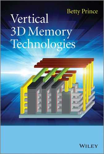
The BiCS NAND flash technology was first discussed by Toshiba in June of 2007. The 3D pipe array structure was intended to increase NAND flash density and was expected to be ready simultaneously with the 32 nm technology node. In the BiCS technology, rather than building transistor layers up vertically one at a time, an entire stack of electrode plates are punched through in one operation. A plug consisting of a string of CT NAND flash transistors is built up in the via holes that are created. This technology permits the number of NAND transistors to be increased without increasing the number of process steps. Figure 4.6 shows a schematic cross-section of the CT NAND flash memory string with vertical CT cells and cross-sections of the vertical field effect transistors (FETs) [3].
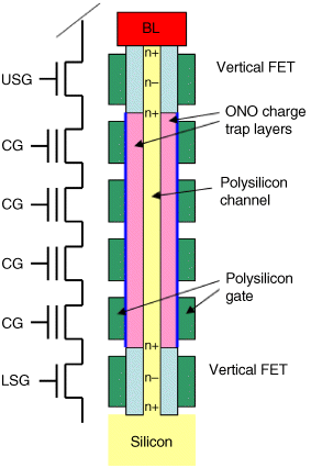
Figure 4.6 Schematic cross-section of the vertical CT cell string and vertical SG FETs. (Based on H. Tanaka et al., (Toshiba), VLSI Technology Symposium, June 2007 [3].)
In this process, after the via holes are punched through the stack, the walls are lightly doped. A vertical n-FET is deposited in the via to form the lower select gate (LSG). This is followed by a GAA CT oxide–nitride–oxide (ONO)-based technology, which is deposited in reverse order along the via walls, forming a series of junctionless CT NAND cells. Finally, another vertical n-FET is deposited near the top of the plug to form the upper select gate (USG). The device density increases with the stack height, but the number of process steps remains the same. This stacked multiple-layer CT memory array has a constant number of critical lithography steps regardless of the number of stacked layers used [3].
The fabrication sequence of the BiCS NAND flash is as follows. The LSG transistor, memory string, and USG transistor are made separately. A stack of alternate dielectric and p+ polysilicon layers is formed. The holes through the gate layers for the transistor channel and memory plug are punched in a single lithography operation, and then low-pressure chemical vapor deposition (LPCVD) tetraethylorthosilicate (TEOS) for the transistor and ONO film for the memory are deposited. The bottoms of the dielectric films are removed by reactive ion etching (RIE), and the remaining hole is plugged by amorphous silicon. Arsenic is implanted and activated for the drain and source of the upper device. The ONO is deposited as 5 nm of LPCVD TEOS film as the top blocking oxide, 11 nm of LP-CVD silicon nitride (Si3N4) film for the trapping layer, and 2.5 nm of LPCVD TEOS film as the tunnel oxide [3].
The edges of the CG are processed into a stair-like structure by repeating the RIE and resist slimming. To minimize disturb, an entire stack of CG and lower select line are etched with a slit, which separates a block of memory plugs from each other. Only the USG is cut into line pattern to work as a row address selector, while the LSG is common to the pillars. Via holes and BLs are made on the array and peripheral circuit simultaneously. The resulting stacked BiCS NAND flash array is shown in Figure 4.7 [3].
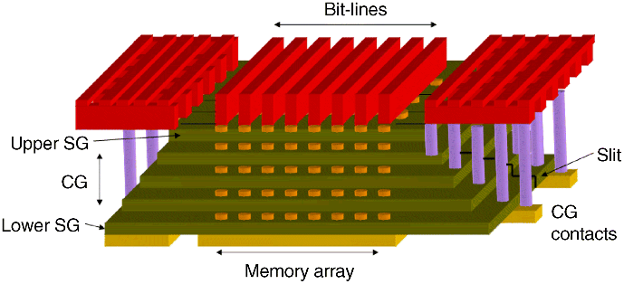
Figure 4.7 3D schematic of stacked BiCS NAND flash array. (Based on H. Tanaka, et al., (Toshiba), VLSI Technology Symposium, June 2007 [3].)
Id–Vg characteristics of the select gate FET were determined. Subthreshold slope was 250 m/dec. Ioff was 30 pA, on-current was 2.4 μA. Endurance to 105 cycles showed a Vth shift of less than 0.5 V after 104 cycles. After 1000 cycles, 2.5 V of the threshold window remained after 10 years [3].
The Toshiba BiCS NAND flash with its stacked vertical array flash memory was discussed by Toshiba again in December of 2007. In 90 nm technology this device had a 6F2 cell array, which is illustrated schematically in the top-down diagram in Figure 4.8 [6].

Figure 4.8 Top-down view of 6F2 cell array of the BiCS flash memory. (Based on Fukuzumi, Y., et al., (Toshiba), IEDM, December 2007 [6].)
When manufacturing this technology, entire stacks of electrode plates were punched through and plugged with polysilicon and other materials at one time. A series of vertical FETs are formed in the punched hole, which act as a NAND string. The vertical GAA FET and the silicon–oxide–nitride–silicon SONS FET memory elements were described in Chapter 3. The memory FETs form a junctionless channel working in depletion mode because they are either undoped or lightly n-doped. This avoids the need to form p-n junctions within the plug. A single bit is accessed at the intersection of a CG plate and a vertical NAND string, which is selected by a BL and a USG. The bottom of the string is connected to the common source diffusion, which is formed on the silicon substrate. In this process, which is punched and then plugged, the order of forming the body, gate dielectric, and gate electrode is reversed compared to the conventional FET. The equivalent circuit of the 3D BiCS NAND flash array is shown in Figure 4.9 [6].

Figure 4.9 Equivalent circuit of 3D BiCS NAND flash. (Based on Y. Fukuzumi, et al., (Toshiba), IEDM, December 2007 [6].)
A 4F2 cell array structure with a double-layered alternate select gate was also described. This technology was based on RIE and damascene processes, so a critical lithography step was not required. The 8-terabit capacity BiCS flash was expected to maintain a bit-cost superiority over 3D layers of stacked horizontal NAND flash [6].
A BiCS NAND flash memory with floating pillars and an oxide–nitride–oxide–nitride (ONON) structure was discussed by Toshiba in December of 2008 [7]. Program and erase operation on the NAND string of the BiCS flash memory was achieved, and it was forecast that this structure could be used for a terabit memory density. Operationally, a single bit of the BiCS flash is accessed at the intersection of a CG plate selected by an USG and a NAND string pillar selected by a BL. The bottom of the pillars is connected to the common source diffusion on the silicon substrate.
A new erase operation was needed because the pillars of NAND string are not connected directly to a p-well. Erase was done by raising the potential voltage of the pillars of the NAND string by injecting holes generated by gate-induced drain leakage (GIDL) at the junction-side edge of the select gate. They found that Vth increased with maximum electric field, showing that the erase operation is caused by hole current generated by GIDL.
Another concern was disturbance of unselected pillars during program or read operation. CGs were shared by several rows of pillars, which also share a USG, as illustrated in Figure 4.10 [7]. The selected USG is shared by selected pillars. The selected CGs are shared by both selected and unselected pillars. This means program/read operation on pillars selected by a USG can result in stress on unselected pillars.

Figure 4.10 Top-down view of BiCS flash memory in program or read operation. (Based on Y. Komori et al., (Toshiba), IEDM, December 2008 [7].)
Despite a large number of stress cycles on unselected pillars, the Vth shift after stress was suppressed by high boost efficiency due to the absence of coupling between pillars of the NAND string and the silicon substrate.
During a read operation, unselected pillars sharing the turned-on LSG plate were connected to the source line. This resulted in those pillars not being boosted. To ensure that the unselected pillars in a read operation could be boosted, a new organization was formed with the LSG plates changed to a “line-and-space” pattern, similar to the USG. This permitted the USG and LSG to be turned on and off synchronously. As a result, the Vth shift after read disturb on unselected pillars was much smaller in the new LSG structure due to the high boost efficiency.
The configuration of shared LSG plate compared with separated line-and-space LSG is illustrated in Figure 4.11 [7].

Figure 4.11 Illustration of shared LSG plate changed to separate line and space LSG. (Based on Y. Komori et al., (Toshiba), IEDM, December 2008 [7].)
The absence of a tunnel barrier film for the ON CT film stack had the potential for retention and disturb issues. For this reason, an ONON film stack was used in which oxide covered by a SiN film was used. The ONON is an SiO2 (blocking oxide)–Si3N4 (charge-trapping)–SiO2 (tunnel oxide)–Si3N4 (tunnel film) vertical stack. The tunnel film in the SONONS structure inhibited release of trapped charge in the SiN and was found to improve data retention and disturb characteristics [7].
4.2.2 Pipe-Shaped BiCS (P-BiCS) NAND Flash Technology
A pipe-shaped BiCS (P-BiCS) flash memory in 60 nm technology was discussed by Toshiba in June of 2009 [8]. The 3D stacked 1Gb cell/layer pipe-shaped flash memory used a 16-cell string. The effective bit cell size was 0.00082 μm2. A branched CG configuration and a new erase operation were used for this memory. The target application was terabit storage devices. The BiCS cell array had multiple stacked CG plates and polysilicon pillars formed through the CG plates. The intersections of the CG plates and polysilicon pillars formed SONOS memory cells. In the original configuration of this cell, the source line was diffused in the silicon substrate and had a high resistance that degraded the read margin. This high-resistance issue was solved in the P-BiCS cell by using a folded pipe structure for the cell string with the source line formed in a metal layer, as shown in Figure 4.12 [8].

Figure 4.12 P-BiCS SONOS NAND flash cell array with vertical pillars. (Based on T. Maeda et al., (Toshiba), VLSI Circuits Symposium, June 2009 [8].)
The cell string consists of two pillars with a pipe connecting the pillars at the bottom. The drain and source select gates now lie over the CG plates. The configuration of the CGs and row decoders was modified to accommodate this new structure. In the original BiCS memory, the CGs were shared by several neighboring rows of cell strings to reduce area. In the new P-BiCS flash, the CG is configured with fork-shaped plates with four branches, where each branch controls two pages of cells. The block is formed by 16 vertically stacked pairs of CGs, with each pair of CG plates arranged in a staggered layout. Select gates are individually separated for the selectivity of cell strings [8].
A further refinement on the P-BiCS vertical NAND flash with 16 stacked layers and MLC operation in 60 nm technology was discussed by Toshiba in June of 2009 [9]. The BiCS flash uses Fowler-Nordheim (FN) tunneling for P/E operations. The FN tunneling originates from the strong curvature effect of the small pipe radius. The P/E characteristics are dependent on the hole diameter, as shown in Figure 4.13 [9], where the 60 nm diameter hole can be seen to have a wider P/E Vth window than the larger diameter holes. The effective cell area per bit is 0.00082 μm2.

Figure 4.13 Vth (V) vs. hole diameter for 20 V P/E voltage for P-BiCS NAND flash. (Based on R. Katsumata et al., (Toshiba), VLSI Technology Symposium, June 2009 [9].)
Device characteristics of the 32Gb P-BiCS NAND flash included a 60 nm complementary metal–oxide semiconductor (CMOS) process, cell size per bit of 0.00082 μm2, memory hole diameter of 66 nm, 16-layer CG stack, and 32 NAND gate string length. The back-end-of-line metallization was three layers of metal including Al–Cu–W. Characteristics of the device included 10-year data retention with no degradation and a Vth shift of less than 0.3 V after 100 000 read cycles at 7.5 V.
Issues addressed by this part included minimizing damage from dilute hydrofluoric acid (HF) treatment for “gate-first” process by using Si3N4-based tunnel film, improving the immunity to read disturb and data retention in order to operate it as an MLC, improving clamping of the high-resistance source line during read operation, and improving control of the diffusion profile of the LSG transistor. The device characteristics of the improved process indicate the potential for MLC operation [9].
The process technology for a U-shaped P-BiCS flash memory were discussed by Toshiba in December of 2009 [10]. An asymmetric S/D profile was used for the select gate and metal salicide for the CG. The select line was low-resistance metal wiring. This resulted in good performance and reliability. The straight-shaped vertical NAND string was changed to a U shape, which improved data retention and widened the Vth window due to less process damage on the tunnel oxide during fabrication. Illustrations of the straight vertical NAND string and the U-shaped NAND string are shown in Figure 4.14 [10].

Figure 4.14 Illustration of the (a) straight vertical; and (b) U-shaped NAND string. (Based on M. Ishiduki et al., (Toshiba), IEDM, December 2009 [10].)
A gate-first deposition process showed good endurance during the P/E sequence. Figure 4.15(a) illustrates the electrode–polysilicon stack, and Figure 4.15(b) shows the stack punched through using RIE to form the memory hole. Figure 4.15(c) shows an ONO film deposited on the walls of the memory hole, and Figure 4.15(d) shows deposition of the body polysilicon and the core filler [10].
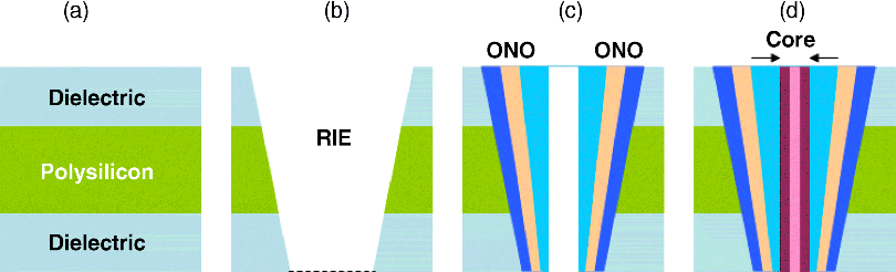
Figure 4.15 Illustration of gate-first deposition process for BiCS flash memory (a) electrode stack; (b) punch through of electrode stack using RIE; (c) ONO film deposited on walls of memory hole; (d) deposition of body polysilicon and core filler. (Based on M. Ishiduki, et al.,(Toshiba), IEDM, December 2009 [10].)
The pipe connection process, which used a sacrificial film, was added to the straight-shaped BiCS, as shown in the schematic cross-section for the P-BiCS flash memory in Figure 4.16 [10].
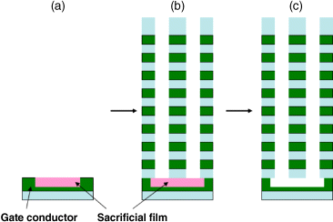
Figure 4.16 Pipe connection process for P-BiCS flash memory showing (a) deposition of sacrificial film; (b) memory hole punch using RIE; and (c) removal of the sacrificial film. (Based on M. Ishiduki et al., (Toshiba), IEDM, December 2009 [10].)
The BL contacts of the BiCS and P-BiCS architectures are shown in the schematic circuit diagram in Figure 4.17 [10]. This diagram shows one 8-cell planar NAND string and four 8-cell vertical NAND strings using the P-BiCs structure. The BL of the P-BiCS has a large number of contacts on a single NAND String. This means the leakage current of the unselected NAND string from BL to source line must be decreased to avoid summing to a larger leakage current and to get a good ON–OFF ratio for the read operation.

Figure 4.17 Circuit schematic of the (a) BiCS; and (b) P-BiCS NAND string showing both number of bit-line contacts and lateral density increase. (Based on M. Ishiduki et al., (Toshiba), IEDM, December 2009 [10].)
An asymmetric source and drain structure was used for the vertical select gate of the P-BiCS flash. Using this structure, holes are effectively generated by GIDL current when source line bias is boosted for the erase operation, while leakage current is suppressed when source line bias is 0 V and the channel pillar is biased slightly positive. An illustration of the asymmetric S/D structure of the select gate (SG) transistor is shown in Figure 4.18 [10].

Figure 4.18 Schematic illustration of asymmetric S/D structure of vertical SG transistor. (Based on M. Ishiduki et al., (Toshiba), IEDM, December 2009 [10].)
Metal salicide deposited with a CVD process was used for the CG of the P-BiCS to lower the resistivity of the doped polysilicon gate. Two orders of magnitude improvement in the sheet resistance was attained. As a result the resistance–capacitance (RC) delay was reduced by an order of magnitude. A test array of the P-BiCS NAND flash array with 1GB of cells per plane was made, and its functionality was confirmed for multilevel data storage [10].
In June of 2010, Toshiba reviewed developments on its P-BiCS flash 3D vertical technology [11]. This process reduces chip cost by stacking the memory array vertically using a punch and plug process. They have shown a pipe-shaped BiCS flash with U-shaped NAND string and MLC operation. The change from a vertical NAND string with a straight-shaped to a U-shaped pipe improved data retention and increased the Vth window because of less process damage on the tunnel oxide during processing. Functionality was shown using a 32Gb test chip with 16 stacked layers and MLC operation in 60 nm technology.
An optimal device structure to solve known issues and improve reliability was shown. The number of contacts per BL was much larger than for a planar NAND device, so the leakage current of the unselected NAND string needed to be reduced to avoid summing up a large leakage in the unselected strings. An asymmetric S/D structure for the select gate was used in which holes were generated by GIDL current when the source line bias was high during erase, but leakage current was suppressed when the source line bias was 0 V and the channel pillar was biased slightly positive. Another improvement was that metal salicide was used with CVD processing for the CG of the P-BiCS.
In April of 2012, Toshiba discussed its roadmap for 2013, which included development of BiCS for NAND and also cross-point arrays [12]. The P-BiCS NAND flash was described as a U-shaped NAND string with a back gate at the bottom of the U to reduce parasitic resistance of the bottom part of the U-shaped pipe. There was no diffusion between the CGs. An undoped polysilicon channel was used for the memory transistors. The select gate used an asymmetric S/D structure to reduce OFF current. An illustration of the P-BiCS NAND flash structure is shown in Figure 4.19 [12].
Figure 4.19 Illustration of P-BICS NAND flash (a) cross-sectional structure; and (b) schematic circuit diagram. (Based on J. Ohshima, (Toshiba), GSA/SEMATECH Memory Conference, 16 April 2012 [12].)
Scaling and device design for a 3D stackable BiCS NAND flash were discussed in May of 2013 by the University of Tokyo [13]. CG length (Lg) and spacing (Lspace) were studied because they could be separately varied in 3D NAND and affect the cell area and electrical characteristics.
A 3D device simulation was used to determine the expected characteristics of Lg and Lspace. It was shown that Lg = Lspace = 20 nm is possible for BiCS-type 3D NAND with a 90 nm diameter hole. Programming voltage can be reduced from 20 to 17 V. Lg and Lspace need to be the same in order to handle the tradeoff between memory window and disturbance. If the number of stacked layers is 18 with a layer pitch of 40 nm, the effective cell size of the 3D NAND corresponds to that of 15 nm planar NAND technology.
In 3D stackable NAND, the number of stacked layers (Nlayer) is increased to reduce the bit cost instead of shrinking the planar cell area. New scaling and design methodologies are required for 3D NAND because they differ significantly from those of planar NAND. A schematic cross-section of the BiCS 3D NAND cell array is shown in Figure 4.20 [13].
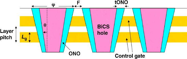
Figure 4.20 Illustration of cell cross-section of BiCS hole. (Based on Y. Yanagihara et al., (University of Tokyo), IMW, 20 May 2013 [13].)
An issue with the 3D NAND is the decrease in cell density in the planar direction. The BiCS hole must by filled with about 20 nm of ONO film. Because the ONO film is not aggressively scaled to maintain the memory window and reliability, the diameter of the BiCS hole is not scalable. For this reason Nlayer should be increased with a finite taper angle “θ” in the BiCS hole, as shown. Because the minimal line-and-space pattern is not required for the CG formation in 3D NAND, the parameters Lcg, Lg and Lspace can be chosen separately. This design flexibility is unique to the 3D NAND for Lg and Lspace. The effective cell area (Aeff) of the 3D NAND was studied, where Aeff = A/Nlayer where A is the cell area in each layer. An expression for Aeff was derived as follows.
Where Rb = the bottom radius of the BiCS hole, Tono is the thickness of the ONO layer, and F is the feature size, which is the spacing between BiCS holes. Aeff of the 3D NAND depends on the cell pitch. Increasing the number of layers becomes less effective for Aeff reduction because the BiCS hole pitch increases with the total height of the 3D NAND in the presence of the BiCS hole taper, as shown in Figure 4.21 [13].

Figure 4.21 Effective cell area vs. number of stacked layers with BiCS hole taper shown between an equivalent planar 15 nm and 20 nm cell areas. (Based on Y. Yanagihara et al., (University of Tokyo), IMW, 20 May 2013 [13].)
The required minimum number of layers (Nlayer) to achieve an Aeff smaller than the planar NAND cell is shown in Figure 4.22 for electrical characteristics achievable by top cell diameter φ = 90 nm [13].
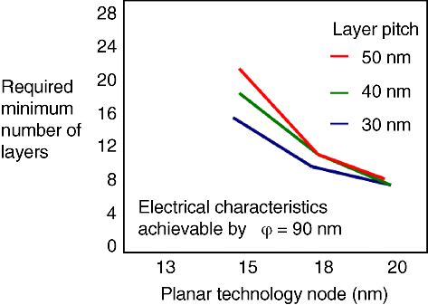
Figure 4.22 Required minimum Nlayer vs. planar technology node by layer pitch. (Based on Y. Yanagihara et al., (University of Tokyo), IMW, 20 May 2013 [13].)
To achieve effective cell size equivalent to 15 nm planar NAND technology, a 40 nm layer pitch with 18 layers is needed. This study explores the Lg and Lspace design window for 40 nm layer pitch. 3D device simulations were done to study their impact on the electrical parameters. Results showed that 3D NAND has good on-current (Ion) and subthreshold slope (SS) compared with the planar NAND. Program voltage (Vpgm) was reduced from 20 to 17 V. Vth roll-off and Vth shift, however, became worse than that of planar NAND below Lg = Lspace = 20 nm in 3D NAND. This was because coupling with the neighboring cell became stronger than in planar NAND. Having the same Lg and Lspace is better for a large memory window and small disturbance. The conclusion was that 3D BiCS-type NAND with effective cell size of 15 nm compared to planar NAND is possible with Lg = Lspace = 20 nm and 40 nm layer pitch if a 90 nm diameter hole is used and the number of stacked layers is 18.
The BiCS technology was reviewed by Toshiba in June of 2013 [14]. The BiCS technology reduces bit cost by using a punch and plug process to vertically stack memory arrays. While the technology is initially being used to stack NAND flash memory, the BiCS technology was expected to be used for other memory devices as well. The BiCS process involves a stack, a punch, and a plug. Multiple layers of plate electrodes and dielectric films are stacked to isolate the various plate electrodes. The multilayer stack is then punched through from top to bottom, with only one lithography step being used. The inside of the holes is then covered with the memory film, and the holes are plugged with vertical pillar electrodes. The memory cells are found at the intersection of the plate electrodes and pillar electrodes. An advantage of using this processing method is that there is no increase in critical lithography, etching, or planarization when layers are added to increase memory density. The basic concept of BiCS is shown in Figure 4.23 [14]. A top-down view cross-section of the GAA memory plug is shown in Figure 4.24 [14].

Figure 4.23 Basic concept of BiCS technology. (Based on A. Nitayama and H. Aochi, (Toshiba), VLSI Technology Symposium, June 2013 [14].)
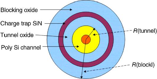
Figure 4.24 Schematic of GAA memory plug cross-section. (Based on A. Nitayama and H. Aochi, (Toshiba), VLSI Technology Symposium, June 2013 [14].)
The study claims that the relative bit cost of the BiCS technology compared to the cross-point array process is as shown in Figure 4.25. As the number of layers increases, the BiCS technology is expected to cost less per bit than the cross-point array technology [14].
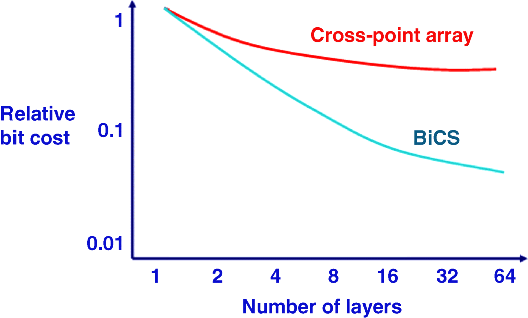
Figure 4.25 Bit cost of BiCS and cross-point array technology by number of layers. (Based on A. Nitayama and H. Aochi, (Toshiba), VLSI Technology Symposium, June 2013 [14].)
3D NAND flash memories have several critical issues that need to be addressed before they can go into scalable mass production. These include WL RC delay, WL and hole formation, data retention, and improvement in cell current. The polysilicon TFT process used in the BiCS flash had improved mobility. The process also has a large electric field contrast due to the difference of channel curvature radius, which permits the blocking oxide to be pure SiO2. The SONOS process has good data retention due to the use of bandgap engineering [14].
4.2.3 Vertical CT Vertical Recess Array Transistor (VRAT) Technology
Mass production of an early 3D vertical NAND flash called the V-NAND was announced by Samsung in August of 2013 [15]. The 128Gb capacity chip was expected to be used in consumer electronics applications such as industrial storage and solid-state drives (SSDs). It used both 3D CT technology and a vertical interconnect process technology to provide twice the scaling of a 20 nm planar NAND flash. In addition to offering higher reliability, it was expected to double the WRITE performance of a planar 10 nm FG NAND flash memory. The device used a vertical interconnect process technology that can stack up to 24 layers vertically using a special etching technology that connects the layers electronically by punching holes from the highest layer to the bottom [15].
The vertical recess array transistor (VRAT) 3D NAND flash memory was discussed in June of 2008 by Samsung and the University of California, Los Angeles [16]. The 3D technology used planarized integration. Another higher-density method of designing 3D NAND flash was also described, which was called the zigzag VRAT (Z-VRAT). A schematic cross-section of the VRAT is shown in Figure 4.26 [16]. The dashed line shows the path the current takes past the four vertical ONO-based CT stacked flash transistors.

Figure 4.26 Schematic of four transistor VRAT NAND Chain (Based on J. Kim et al., (University of California Los Angeles, Samsung), VLSI Technology Symposium, June 2008 [16].)
The VRAT structure increases memory density through stacking multiple layers. Fully depleted channels permit keeping the gate length unscaled to help suppress subthreshold leakage current (SLC). Vertical interconnects are formed at the same time as the VRAT array, which helps reduce cost.
The VRAT consists of vertically chained transistors and interconnects. Multiple stacks of nitride and undercut oxide layers are covered with a thin, fully depleted polysilicon channel. The channel length is maintained due to its recessed shape, while the double-gate structure increases the drive current. A tilt-angle n-type implantation is used to dope the channels [16].
The process sequence is illustrated in Figure 4.27 [16]. In this sequence, multiple alternating layers of oxide and nitride films are deposited partially sloping up a silicon mesa. These are patterned lithographically and etched to form the active region (Figure 4.27(a)). These oxide layers are then selectively etched with a wet process to form an undercut (Figure 4.27(b)). The polysilicon is then deposited to form the channel material of the active transistors (Figure 4.27(c)). A nitride CT material is deposited in the undercut between the tunnel oxide and the control oxide to form the ONO followed by the WL electrodes. An etch-back removes the WL electrode material on the sidewall, leaving the WL electrodes in the undercut space but isolated from one another (Figure 4.27(d)). Planarization using CMP exposes the gate electrodes in a horizontal plane on the slope (Figure 4.27e). N-type implant is done at a tilt angle to form the S/D, and each string is isolated (Figure 4.27(f)). Contacts are then completed (Figure 4.27(g)) [16].

Figure 4.27 Process Sequence for the VRAT NAND flash. (Based on J. Kim et al., (University of California Los Angeles, Samsung), VLSI Technology Symposium, June 2008 [16], with permission of IEEE.)
4.2.4 Z-VRAT CT Memory Technology
It was estimated that memory density of 128Gb could be obtained with the VRAT in 50 nm technology. A further increase in memory density can be obtained potentially by splitting a VRAT into two narrow mesas through the middle, which doubles the memory density. A Z-VRAT with eight transistors in a vertical stack was simulated, and a zigzag current path was shown along the polysilicon channel. Samsung estimated that a NAND flash memory density as high as 256Gb could be obtained using the Z-VRAT in 50 nm technology with 16 stacks. A schematic cross-section of the Z-VRAT with a six-transistor vertical string is shown in Figure 4.28 [16].
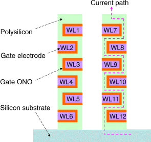
Figure 4.28 Schematic cross-section of Z-VRAT with six transistors in vertical string. (Based on J. Kim et al., (University of California Los Angeles, Samsung), VLSI Technology Symposium, June 2008 [16].)
In the Z-VRAT process, the polysilicon on the top is removed, and the oxide/nitride layers are etched using a wet process. The gate electrode is filled, planarization is done to form the contacts, and finally the contacts and metal connections are formed. An illustration of the 3D Z-VRAT technology is shown in Figure 4.29 [16].
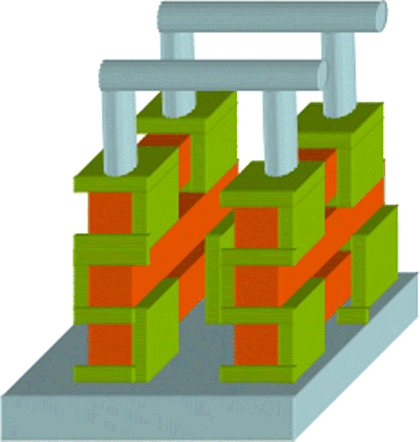
Figure 4.29 Illustration of 3D Z-VRAT technology. (Based on J. Kim et al., (University of California Los Angeles, Samsung), VLSI Technology Symposium, June 2008 [16].
A comparison of possible memory density at the 50 nm node was done for the planar, VRAT, and Z-VRAT array architectures and is shown in Table 4.3 [16].
Table 4.3 Comparison of Memory Density at 50 nm for Planar, VRAT, and Z-VRAT Arrays.
| Planar | VRAT | Z-VRAT | |||
| Density (Gb) | 16 | 64 | 128 | 128 | 256 |
| Layers | 1 | 8 | 16 | 8 | 16 |
| MLC/SLC | MLC | SLC | SLC | SLC | SLC |
| Based on J. Kim et al., (UCLA, Samsung), VLSI Technology Symposium, June 2008 [16]. | |||||
4.2.5 Vertical NAND Chains—VSAT with “PIPE” Process
A vertical stacked array transistor (VSAT) that was combined with a PIPE process (Planarized Integration on the same PlanE) was discussed by Samsung in June of 2009. The full PIPE method of vertical interconnection was thought to be an improvement over the “stair-like” PIPE connection method used previously for cost effectiveness, measured in lateral area of silicon and in simplicity of manufacture. A schematic diagram of the two interconnection methods is shown in Figure 4.30. The vertical interconnection method is deposited on a sloping surface and planarized to expose the pipes at the surface [17].
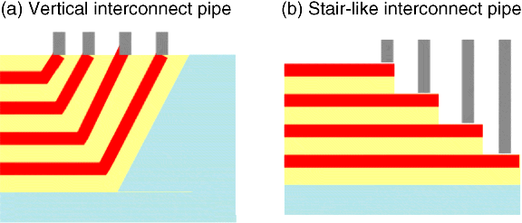
Figure 4.30 Vertical interconnection “PIPE” vs. “PIPE stairs.” (Based on J. Kim et al., Samsung, VLSI Technology Symposium, June 2009 [17].)
The 24-transistor VSAT NAND string is formed using three vertical stacks with eight devices per stack. The BL contacts four devices on one side of the stack and four devices on the other side of the stack. Devices on opposite sides of the stack share a common WL. A schematic diagram of the VSAT and PIPE is shown in Figure 4.31 [17]. This method of forming vertical NAND chains decreased the off-current level in the polysilicon channel transistor by five orders of magnitude by using a thin 20 nm body and a double-gate-in-series structure. Hydrogen annealing was used to improve the subthreshold swing and mobility of the polysilicon channel transistor. The VSAT + PIPE NAND technology was thought to be an improvement over the previously shown VRAT + PIPE 3D NAND structure, which created an undercut space and filled it with electrodes. Improvements in subthreshold performance and channel mobility also resulted from using a thinner polysilicon channel [17].
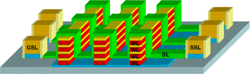
Figure 4.31 Schematic cross-section of VSAT + PIPE technology along with bit-line. (Based on J. Kim et al., (Samsung), VLSI Technology Symposium, June 2009, Figure 3 [17].)
An equivalent circuit diagram showing the VSAT device with three vertical strings is shown in Figure 4.32 [17]. This device was developed at the 100 nm node. Storage capacity was expected to reach 128GB with 16 multiple layers on the 50 nm node [17].
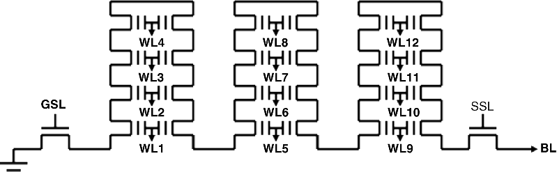
Figure 4.32 Equivalent circuit diagram of VSAT NAND flash with three vertical strings. [17] (Based on J. Kim et al., (Samsung), VLSI Technology Symposium, June 2009, Figure 6 [17].)
4.2.6 Vertical CT PIPE NAND Flash with Damascene Metal Gate TCAT/VNAND
A damascene tungsten (W) metal gate CT cell in a 3D vertical NAND flash string was proposed by Samsung in June of 2009 [18]. It was called a terabit cell array transistor (TCAT) and was made by a gate replacement process. Bulk erase operation of the cell was demonstrated. A schematic cross-section of the Samsung TCAT vertical NAND flash string structure with details of the selection transistors is shown in Figure 4.33 [18].
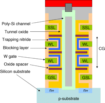
Figure 4.33 Schematic cross-section of Samsung vertical NAND flash string structure (TCAT). (Based on J. Jang et al., (Samsung), VLSI Technology Symposium, June 2009 [18].)
The cell string has six NAND cell transistors with a string select (SSL) transistor on top and a ground select line (GSL) transistor on the bottom. The SSL and GSL transistors are formed at the same time as the cell transistors are. The TCAT vertical NAND flash technology with metal gate and bulk erase operation was projected as a potential technology for terabit memory capacity. A 32-string array was characterized. The subthreshold slope was about 320 mV/dec and on–off ratio was >106. A good threshold distribution was attributed to the GAA body effect. Program disturb was suppressed by Vth adjustment of select transistors [18].
Samsung has indicated that its TCAT process solves several of the issues with the earlier Toshiba BiCS stacked NAND string technology. This included a potential difficulty in etching the metal–oxide multilayer simultaneously and a concern that a circuit change might be necessary to apply negative bias on the WL during erase to avoid potential GIDL erase.
The process sequence is as follows: initially an oxide–sacrificial nitride multilayer stack is deposited, the channel hole is etched and filled with polysilicon, gate pads are etched to form a pyramid-like stack that provides access for contacts to the WLs, the WL cut is dry etched to separate the vertical device strings and the sacrificial nitride is removed by wet etching, a gate dielectric (ONO) is deposited, and a common source line (CSL) implant is done followed by deposition of the tungsten WLs. Contacts to the WL steps are formed in the back-end-of-the-line process [18].
The TCAT NAND flash memory is capable of bulk erase operation because the channel poly plug in the TCAT structure is connected to the silicon substrate so that conventional bulk erase operation can be performed and the NAND string can be operated without a significant change to the conventional peripheral circuitry used in the planar flash. Erase saturation at about 1 V was an issue but was expected to improve with a channel hole diameter of 45 nm, which will cause the electric field in the tunnel layer to become stronger. A 120 nm hole diameter was used in this test device. Endurance was 104 cycles, and data retention at 85 °C showed a Vth window of 5.6 V after 10 years. This was expected to permit MLC operation [18].
Further efforts on its 3D NAND TCAT technology with a 90 nm channel hole were discussed by Samsung in June of 2010 [19]. The TCAT was improved by the addition of damascened metal gates, which provided low resistance. A new tungsten fill metal process was adopted to reduce WL resistance by increasing the portion of low-resistivity tungsten in the metal gate. The resistance was reduced by more than 70% over the conventional process without changing the dimension of the gate. Lowering the WL resistance improves the performance of NAND devices in a given chip area or permits reducing chip size without affecting performance.
Lateral charge spreading was decreased by a biconcave structure that could be achieved by using a damascened gate structure. A controlled offset between the BL contact and the select transistor was also used. A suppressed disturbance property was achieved by using this offset, which reduces the leakage current through the select transistor. A comparison of the trap layer structure of the (a) BiCS 3D NAND and (b) concave TCAT VNAND device is shown in Figure 4.34 [19]. The electric field induced between adjacent cells that are programmed in different states tends to accelerate charge losses at high temperature. The biconcave TCAT structure helps prevent lateral charge losses.

Figure 4.34 Trap layer structure of (a) BiCS 3D NAND; and (b) TCAT 3D NAND. (Based on W.S. Cho et al., (Samsung), VLSI Technology Symposium, June 2010 [19].)
With scaling from 120 to 40 nm channel width, the electric field induced in the tunnel layer is increased, while the field in the blocking layer is reduced as the diameter of the channel hole is scaled. For a 90 nm channel width, a Vth window of about 7 V was achieved using Vpgm = 18 V and Vers = −18 V, as shown by the P/E characteristics in Figure 4.35 [19]. Data retention after 10 years showed less than a 0.5 V shift in Vth window.

Figure 4.35 Program and erase characteristics of a 90 nm channel width VNAND. (Based on W.S. Cho et al., (Samsung), VLSI Technology Symposium, June 2010 [19].)
Reliability of the TCAT VNAND CT Flash arrays was simulated by Samsung in June of 2012 [20]. Two intrinsic variation sources of the cell threshold voltage induced by traps in the polysilicon channel material in a 3D VNAND flash using CT were described. These variation sources were random trap fluctuations (RTF) and random telegraph noise (RTN). RTN was shown to be enhanced by the polysilicon material used for the channel. A model was developed that explained the asymmetric RTN distribution observed after endurance testing. The model enabled prediction of Vth distribution for VNAND devices during MLC operation.
RTF is due to fluctuations of a trap location inside the polysilicon channel. These traps were shown to follow a Poisson statistic, and it was shown that trap density was the correct metric for evaluating the electrical performance of the polysilicon channel. RTN follows an exponential distribution due to RTF in polysilicon. The RTN energy distribution indicated that most of the RTN traps were present at the Fermi level. It was found that cycling the cell induced a generation of RTN traps during programming. The model used was found suitable for the complex 3D structure and permitted structure optimization and statistical prediction for the vertical NAND structure. It also modeled accurately the MLC distribution, permitting prediction of the ECC requirements for the VNAND [20].
4.2.7 3D NAND Flash SB-CAT Stack
In December of 2011, Seoul National University discussed a 3D stacked NAND Flash which used a common gate structure and a shield layer. A trench structure was used instead of a through-hole structure. The 3D structure is called a Square wave-shaped BL cell array transistor (SB-CAT). A 2-D schematic is shown in Figure 4.36 [21].

Figure 4.36 3-D stacked NAND flash using trench structure with shield. (Based on M.K. Jeong et al. (2011) (Seoul National University), IEEE Transactions on Electron Devices, 58(12), 4212 [21].)
The trench structure permitted Vth variation in cells of a NAND cell string to be reduced and the number of stacked control-gate electrodes in a gate stack was increased. In the trench between adjacent CG stacks, gate O/N/O stack, poly-Si body, backside oxide and shield layer were formed. The 3D stacked cell strings had three layers of vertically stacked CGs. Vth was controlled by applying bias to the shield layer. Reasonable cycling and retention and good pass-gate properties were shown in the bottom of the trench. The n+ region in the bottom of the cell can count as a CG in the bottom cell. Two layers of CG's were used in the structure [21].
The SB-CAT structure, by using common CG and shield layer, assures an effective cell area of 4F2/n. A cell string is made with three layers of electrodes which includes two selection devices, SSL and GSL, and four cells. Using the trench for isolating adjacent stacks means the stacking of electrodes is more expandable than a conventional through-hole-type structure. The cell string showed retention window of 0.84 V after 10 years and cycling with Vth shift of 1.5 V after 5 × 10³ P/E cycles. The cell in the bottom of the trench was confirmed to work well so that both vertical surfaces could be connected successfully by turning on the bottom cell. By controlling the bias of the trench shield, the cell threshold voltage shift could be controlled for both program and erase states [21].
A study of the ID-VGS characteristics of a 3D stacked NAND flash string with a common gate and a shield layer was discussed in May of 2010 by Seoul National University [22]. Body cross-talk was eliminated completely. The proposed common gate and shield layer structures were thought to be promising for future vertical NAND flash string memories.
4.3 3D FG NAND Flash Cell Arrays
4.3.1 3D FG NAND with Extended Sidewall Control Gate
Several efforts have been made to use FG NAND flash cells in vertical channel arrays. This technology development is an attempt to extend the conventional FG structure into the 3D architectures.
Arrays made with the extended sidewall control gate (ESCG) FG cell were discussed in May of 2010 by Tohoku University [23]. In this cell, the S/D region has an electrically inverted layer caused by an extended sidewall CG. The surface electron density of the S/D is higher than that of a conventional FG cell with diffused S/D. The result is a low-resistive S/D. The ESCG cell uses enhancement mode operation. The cylindrical FG structure cell with the extended sidewall CG was intended to overcome various issues possible with CT cells, such as charge spreading, which can reduce the Vth window for MLC operation.
A 4-bit vertical FG NAND cell array using the ESCG cell along with an equivalent schematic circuit diagram of the cell array is shown in Figure 4.37 [23]. Normal flash cell operation with fast programming and high read current was achieved as a result of the increased coupling ratio and the low-resistive S/D technique. The 3D vertical flash memory cell array with the new S/D technique had about 50% less interference with neighboring cells than the planar FG NAND cell. This cell array was considered a potential candidate for a fast and reliable terabit 3D vertical NAND flash cell array.

Figure 4.37 Schematics of (a) a 4-bit vertical FG NAND cell array with ESCG; and (b) an equivalent circuit diagram. (Based on M.S. Seo, S.K. Park, and T. Endoh, (Tohoku University), IMW, 16 May 2010 [23].)
The interference effects of direct and indirect coupling paths of neighboring cells for 3D FG NAND cell arrays with an ESCG cell structure were discussed in June of 2011 by Tohoku University and JST-CREST [24]. The 3D NAND cell array structure with ESCG was shown to fully suppress the interference effects. With the ESCG cell structure, the FG is formed cylindrically and fully surrounded by the CG. Conventional electrical S/D techniques can used with the ESCG structure.
Capacitive coupling effects between adjacent FGs are illustrated in Figure 4.38. Figure 4.38(a) illustrates the coupling capacitance between adjacent FGs for the conventional FG structure, and Figure 4.38(b) illustrates the coupling capacitance between adjacent FGs for the ESCG cell [24]. Due to the coupling of the ESCG shielding structure, the FG–FG capacitance is suppressed.
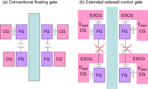
Figure 4.38 Illustration of capacitive coupling effects of (a) conventional FG cell; and (b) ESCG cell. (Based on M.S. Seo and T. Endoh, (Tohoku University, JST-CREST), VLSI Technology Symposium, June 2011 [24].)
With the ESCG cell structure, the FG–FG coupling capacitance was sufficiently suppressed, and the CG coupling capacitance was increased due to the increase in area between the CG and the FG. For the ESCG cell, the interference is mainly due to the direct coupling from neighboring FGs to the ESCG channel region. In order to efficiently suppress the direct coupling effect, the ESCG is controlled by applying a fixed bias. Using 3D simulation, the interference of the optimized ESCG cell was found to be suppressed below 50 mV.
The 3D vertical FG NAND flash memory cell array with ESCG was compared to a 3D vertical FG cell without the ESCG in September of 2011 by Tohoku University and Hynix [25]. The ESCG structure allowed enhancement mode operation. Normal flash cell operation was shown to have fast programming and good read current due to the increase in coupling ratio and the use of an ESCG low-resistive electrical S/D technique. A 3D vertical NAND flash cell array with ESCG had about 50% less interference with neighboring cells than a conventional 3D vertical FG NAND without the ESCG. A 3D NAND flash array with ESCG showed fast read and program and good reliability.
Using the ESCG structure, both enhancement mode operation and conventional bulk erase were achieved. Figure 4.39 shows a cross-sectional view of both the conventional FG and the proposed ESCG [25]. The FG is formed cylindrically and surrounded by the CG. An electrical S/D is formed in the junctionless channel when a positive bias is applied to the ESCG structure. At the surface of the pillar, the electrically inverted electron density of the ESCG cell was found to be higher than that of the conventional FG cell with a diffused S/D by about an order of magnitude.

Figure 4.39 Cross-section of (a) conventional FG cell; and (b) ESCG cell. (Based on M.S. Seo, S.K. Park, and T. Endoh, (Tohoku University, Hynix), IEEE Transactions on Electron Devices, 58(9) [25].)
Cross-sectional views of the conventional FG and ESCG cell during bulk erase are shown in Figure 4.40 [25]. The diffusion S/D junctions of the conventional FG device may change the silicon pillar potential when the bulk erase bias propagates into the channel. With the ESCG cell, when the positive erase bias is applied in the channel region, holes accumulate at the surface of the pillar region, and no S/D junction exists. This means the erase potential is transferred to the entire pillar region so that normal bulk erase occurs.

Figure 4.40 Schematic cross-section during bulk erase of (a) a conventional FG cell; and (b) an ESCG cell. (Based on M.S. Seo, S.K. Park, and T. Endoh, (Tohoku University, Hynix), IEEE Transactions on Electron Development, 58(9) [25].)
The conclusion was that even though the ESCG FG cell size is larger than the vertical CT NAND flash cell, an MLC operation can be done without coupling effects with neighboring cells. This MLC operation can potentially improve the bit cost and provide superior reliability characteristics [25].
4.3.2 3D FG NAND with Separated-Sidewall Control Gate
A 3D vertical polysilicon pillar FG NAND flash memory cell array using a separated-sidewall control gate (S-SCG) was proposed by Tohoku University and Hynix in May of 2011 [26]. This cell has a cylindrical FG with a line-type CG and an S-SCG structure.
With the S-SCG NAND cell array, the same operating conditions can be achieved as in the conventional planar FG NAND. Bulk erase is realized by using an electrically inverted S/D technique. To prevent direct interference and disturbance issues, the voltage levels in the SCG regions were controlled to 8 V in program, 0 V in erase and 3.5 V in read operation. The S-SCG cell array fully suppressed both the interference effects and the disturbance problems by removing the direct coupling effect in the same cell string. The cell was thought to have good potential for a terabit 3D vertical NAND flash cell array with MLC operation.
Figure 4.41 illustrates the structure of various vertical channel FG cells including the conventional FG cell, the ESCG cell, and the S-SCG cell [26].

Figure 4.41 Various types of FG vertical channel cell structures: (a) conventional FG; (b) ESCG; and (c) S-SCG. (Based on M.S. Seo et al., (Tohoku University, Hynix), IMW, 22 May 2011 [26].)
A 3D vertical FG NAND flash array using the S-SCG was discussed further in August of 2012 by Tohoku University and Hynix [27]. This cell used a cylindrical FG with a line-type CG with S-SCG structure. Normal flash cell operation was shown, and the performance was found better than various other 3D FG NAND cells by using a cylindrical device simulation. The study showed that the proposed cell could reach a high CG coupling ratio. The cell programmed at 15 V with Vth = 4 V and erased at 14 V with Vth = −3 V. The retention mode electric field was good, and there was sufficient read-mode on-current margin.
The benefit of the 3D vertically stacked S-SCG addressed in this study was MLC operation. This operation could significantly increase the bit density and reduce the bit cost of the array, compensating for the larger cell size of the FG vertical channel cells. Key factors in MLC operation were the distribution of the programmed Vth and the Vth shift. All of the 3D vertical channel NAND arrays have a bit cost that is inversely proportional to the number of stacked cells. MLC operation is an issue with the CT NAND cell, which has difficulties with charge spreading and with retention characteristics. The distribution of the programmed Vth is affected by interference and disturbance issues. Other issues are direct coupling effects from neighboring cells in the same cell string.
Process complexity was a significant factor in stacking cells, and the scaling was limited by high-voltage cell operations, which could limit scaling in sub–10 nm technology due to the fixed dielectric thickness of about 20 nm, which included tunnel oxide and interpoly dielectric layers. High program voltage was a critical issue because it was applied directly to the sidewall CG. This study showed the superior cell performance of the S-SCG NAND cell including low-voltage P/E operation, good retention mode electric field, fully suppressed interference, direct disturb issues, and sufficient read-mode on-current margin.
The ESCG structure discussed previously suppressed the interference coupling effect so that high CG coupling capacitance could be obtained and the S/D structure could electrically invert the pillar at the same time. Direct disturb to neighboring passing cells, however, remained an issue as a result of the high coupling capacitance in the ESCG. This issue was addressed by the S-SCG structure. A schematic cross-sectional view of the S-SCG array is shown in Figure 4.42 [27].
Figure 4.42 S-SCG array cross-section. (M.S. Seo, B.H. Lee, S.K. Park, and T. Endoh (2012) (Tohoku University, Hynix), IEEE Transactions on Electron Development, 59(8), 2018 [27].)
In a 20 nm–type technology, the S-SCG horizontal feature size was about 24 F2 (6F × 4F), and the vertical height was 2F, resulting in a cell volume of about 48 F3. This height could be achieved by using a thin, prestacked SCG. The common SCG method was applied in order to minimize the number of contacts, as shown in the equivalent circuit of the cell arrays in Figure 4.43 [27].

Figure 4.43 Equivalent circuit diagram of the S-SCG cell array. (Based on M.S. Seo (2012) (Tohoku University, Hynix), IEEE Transactions on Electron Development, 59(8), 2018 [27].)
The operating conditions of the S-SCG cell array were similar to the conventional planar FG NAND. The conventional bulk erase and program inhibit operations were obtained by using an electrically inverted S/D and using an efficient channel-boosting ratio. Medium voltage levels were applied to the SCG regions, such as 11 V during program operation. The Vscg during the read operation was minimized to 1 V in order to increase the initial Vth when the FG had no charge.
The process included two different layers. The polysilicon layers were deposited, the pillar and FG regions were cylindrically etched, and then barrier oxide was deposited. The cylindrical FG region was deposited using a unidirectional etch process, and then tunnel oxide and polysilicon pillar were deposited. The CG was then self-aligned by using an etching ratio and a silicide process. The self-aligned process used the difference of the etch ratio between the two deposited layers [27].
To evaluate the characteristics of the S-SCG cell, 2D device simulations were used together with cylindrical coordinates in the vertical direction. An eight-cell NAND string was used to simulate an unselected cell. The mobility coefficients were decreased using a constant mobility model to indicate mobility degradation by trap density in the polysilicon pillar region. The amount of charge in the FG region was controlled by using a nonlocal tunneling model. Cylindrical device simulations were done on a 30 nm cell to obtain FG coupling capacitance, P/E voltage, disturbance and interference issues, read on-current, and retention mode E-field. In the S-SCG cell model it was found that the program voltage improved as the Vscg was increased, and the erase voltage improved as Vscg was decreased. Even if only half of the conventional program voltage is applied to the SCG node, the S-SCG NAND cell still had low-voltage P/E operations as a result of its excellent coupling ratio [27].
Disturb becomes more of an issue with the high CG coupling ratio used in many 3D vertical NAND cell arrays—particularly when the high program voltage is directly applied to the SCG. In addition, the high SCG voltage limits the vertical scaling. With the S-SCG cell, however, the Vscg level can be controlled by using an independent SCG. The Vread or Vpass and Vscg can be combined to prevent direct disturb problems. To maintain reliability of the interpoly dielectric (IPD), the voltage difference between CG and SCG was maintained below 9 V. This means Vscg can be increased to 11 V with Vpass at 2 V during program to improve the program efficiency. Vread can also be 10 V with Vscg at 1 V during the read operation to reduce external resistance of the neighboring cells [27].
The feasibility of having an MLC and the number of stacked cells obtainable compared with conventional 3D cells was addressed. The S-SCG cell fully suppressed both the interference effect and the direct disturbance issue. It had a low E-field in retention mode, which indicated good potential for highly reliable MLC operation with an FG cell. The vertical cell height was decreased compared to other vertical NAND cells by using a predeposited thin S-SCG and applying medium-level bias [27].
4.3.3 3D FG NAND Flash Cell with Dual CGs and Surrounding FG (DC-SF)
A 3D dual control gate with surrounding floating gate (DC-SF) NAND flash cell was discussed by Hynix in December of 2010 [28]. This structure provides a high coupling ratio, low-voltage operation with program at 15 V and erase at −11 V, and a wide P/E window of 9.2 V. FG-to-FG interference was a low 12 mV/V due to the CG shield effect. The device was multibit with 2 bits/cell or 4 bits/cell. In this structure, one surrounding FG is controlled by two neighboring CGs. This arrangement results in an improved coupling ratio due to the larger surface area between the FG and the CGs. The structure is scalable in the horizontal direction. There is no FG-to-FG interference in a string because the CG was between the two FGs and acted as a shield. The device had a 9.2 V P/E window that permitted MLC operation.
A method for read operation for a 3D DC-SF NAND flash memory was discussed in May of 2011 by Hynix [29]. A single-cell cross-section is shown in Figure 4.44(a), and a schematic cross-section of an array is shown in Figure 4.44(b).
Figure 4.44 3D dual control gate with surrounding FG NAND string. (Based on H.S. Yoo et al., (Hynix), IMW, 22 May 2011 [29].)
Based on the model used, the selected cell Vth was increased by the neighbor cell's high Vth because the neighbor cell does not have enough Vpass-read to be a pass transistor in a conventional read operation. To prevent this neighboring-cell high Vth effect, a higher Vpass-read is applied to the CG of the neighbor cell, and a lower Vpass-read is applied to the CG of the next neighbor cell to compensate for the FG potential of the neighbor cell. For read operation of an MLC, the Vpass-read modulation must be decreased in correspondence to the selected cell read voltage. Using this new read scheme, a stable read operation was achieved for 2 bits/cell and 3 bits/cell operation [29].
A 3D NAND flash memory that used a metal control gate last (MCGL) process for a DC-SF cell was discussed by Hynix in June of 2012 [30]. This process corrected several issues identified in previous DC-SF cells. The MCGL process used a low-resistive tungsten metal WL with high-κ IPD, resulting in low damage on the tunnel oxide/IPD and a preferable FG shape. A conventional bulk erase could be used due to the direct connection between channel poly and the p-well by the channel contact holes. It was projected that up to 3-bit MLC configurations could be made using this technology, which would permit 512Gb 3D NAND flash memories.
In the previous DC-SF cells, there were several problems identified: high WL resistance of the poly gate, damage on IPD ONO by FG separation, FG field confinement at the FG edge during programming, and issues caused by GIDL erase. This study proposed a new MCGL process that was intended to solve these issues.
The MCGL process avoided some of the drawbacks of the conventional DC-SF process, as illustrated in Figure 4.45. Figure 4.45(a) shows the conventional DC-SF process that used ONO IPD and poly CGs. This process suffered from IPD damage, lack of FG field confinement at corners, and high WL resistance. The new MCGL process is illustrated in Figure 4.45(b). It has straight tunnel oxide, which avoids corners, and uses a high-κ IPD to resist damage and a low-resistance tungsten WL [30].

Figure 4.45 Schematic cross-section of (a) conventional DC-SF process showing issues with this process; and (b) MCGL process showing improvement in these issues. (Based on Y. Noh et al., (Hynix), VLSI Technology Symposium, June 2012 [30].)
The MCGL process had a shorter distance between substrate and LSG, which produced a high saturation current by reducing the parasitic resistance in the string. The P/E window was 8 V. Neighbor cell program disturbance was reduced because Vpass for the neighbor cell was decreased during program. The cell-to-cell FG-to-FG interference was 30 mV/V due to shielding effects of the tungsten WL. For program and erase cycles, the Vth shift after cycling was less than 1.3 V after 1000 cycles. Data retention testing showed a shift of 60 mV after a 250 °C 120-minute bake, which is comparable to planar FG NAND. To avoid source line bounce issues during read, the SL contact was made 1 contact per 128 strings [30].
The MCGL process developed to improve performance and reliability of the DC-SF cell was discussed further in April of 2013 by Hynix and Hiroshima University [31]. Read and program operation schemes were developed. In the read operation, both higher and lower Vpass-read were alternately applied to unselected CGs to compensate for lower FG potential to a pass transistor. In the program scheme, the optimized Vpass was applied to a neighboring WL or the selected WL to prevent program disturb and charge loss through IPD. The use of the MCGL process and new read and program methods permitted a higher-performance, more reliable DC-SF cell for use in 3D NAND flash memories [31].
The conventional read operation for the DC-SF NAND flash string involved applying the read voltage (Vr) to the two neighboring CGs of the selected FG and applying Vpass-read to unselected CGs. Vr was a predetermined value for cell read. The MLC read operation is defined as shown in Figure 4.46 [31].
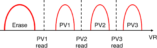
Figure 4.46 Illustration of levels for MLC read operation. (Based on S. Aritome et al. (2013) (Hiroshima University, Hynix), IEEE Transactions on Electron Devices, 60(4), 1327 [31].)
A new read operation was developed for the DC-SF NAND string. For each Vr for PV1, PV2, and PV3, Vpass-read2 and Vpass-read1 should be different voltages to compensate for the neighboring FG1 potential. This new read operation is illustrated in the schematic circuit diagram in Figure 4.47(b), where Vpass-read1 and Vpass-read2 have a dependence on Vr as shown the graph in Figure 4.47a [31]. The operating voltages for the new read method for the DC-SF NAND string for various values of Vr were specified.

Figure 4.47 Read of the DC-SF NAND string: (a) Vpass vs. VR(V); and (b) schematic circuit diagram of Vpass-read vs. VR. (Based on S. Aritome et al., (Hiroshima University, Hynix), IEEE Transactions on Electron Devices, 60(4), 1327 [31].)
The programming method for a DC-SF cell needed to be optimized to avoid program disturb issues. There are two inhibit modes for the DC-SF cell: the electron injection mode and the charge loss mode. The electron injection mode had a weak electron injection stress caused by a high field in the tunnel oxide due to the FG coupled with two CGs. This mode became an issue in the erase state (at lower Vth) because of the high field of the tunnel oxide. The charge loss mode is unique to the DC-SF cell in that electrons in the FG are ejected to the CG by the high field in the IPD. This mode becomes an issue with high cell Vth. To minimize program disturb issues, Vpass_n − 2 and Vpass_n + 2 must be optimized. P/E cycling showed Vth shift after cycling is less than 1.3 V after 1000 cycles. Data retention was found comparable with conventional planar FG NAND flash.
4.3.4 3D Vertical FG NAND with Sidewall Control Pillar
A 3D vertical FG NAND flash cell array using a sidewall control pillar (SCP) was discussed in May of 2012 by Tohoku University and Hynix [32]. This cell had a cylindrical FG and a SCP with a line-type CG, as shown in Figure 4.48 [32]. The SCP structure is connected to the NAND string's polysilicon pillar on both sides of each FG. A tight vertical space length is achieved by using a self-aligned process for deposition of the polysilicon pillar. The SCP NAND cell has the same operating conditions as the DC-SF NAND cell. To compensate for the increase in channel capacitance, the FG width was decreased by 15 nm and a high-κ material was used for the IPD. The cell programmed at 18 V with Vth = 4 V and erased at 17 V with Vth = −3 V, which was comparable to conventional FG NAND cells. The same vertical scaling found with a CT 3D NAND cell was achieved for sub–20 nm technology. This cell was expected to have potential for use in a terabit 3D vertical NAND cell.
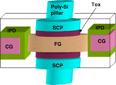
Figure 4.48 3D FG NAND cell with SCP. (Based on M.S. Seo, J.M. Choi, S.-K. Park, and T. Endoh, (Tohoku University, Hynix), IMW, 20 May 2012 [32].)
Vertical scaling of 3D FG NAND cell arrays was limited by the interference with neighboring cells. As a result several 3D vertical FG NAND cells with an SCG that reduces the interference issue of the FG NAND cell have been shown. These vertical FG NAND cells have such features as ESCG, DC-SF, and separated SCG. To suppress the interference coupling effect of the FG-type cell, the SCG is used. High program speed is achieved due to the increased coupling ratio of the SCG. Cells with FG NAND SCGs, however, have issues in both neighboring passing cell disturb and reliability of the IPD next to the SCG because high operating voltage is applied to the SCG during P/E operations. The SCG NAND cell has difficulties scaling vertically below 30 nm because it is limited by SCG and IPD thickness.
The operation of the 3D vertical FG NAND cell with SCP was compared with 3D FG NAND cells with the SCG structure, including the ESCG, DC-SF, and S-SCG. 3D cylindrical device simulations of an eight-cell NAND string were performed to determine the characteristics of the SCP NAND cell. The simulation assumed FN tunneling for the FG-type NAND cell. For the SCP NAND cell, two kinds of interference effects were found to exist. These are conventional indirect coupling between FGs and direct coupling from FG to SCP. These effects depend on parameters such as the length and width of the SCP (Lscp, Wscp) and the width of the FG (Wfg). The read current and interference effects for the cell as a function of Wscp/Wfg are shown in Figure 4.49(a), where the Iread and interference ΔVth depend on the ratio of Wscp/Wfg, where Wfg = 30 nm. This ratio is minimized at 60%. If Lscp is decreased, interference worsens due to the coupling effect with the neighboring FG while the Iread improves due to the channel resistance of the SCP. Corner effects were also shown to exist and be optimized. The Iread and interference ΔVth dependence on Lscp are shown in Figure 4.49(b) [32].
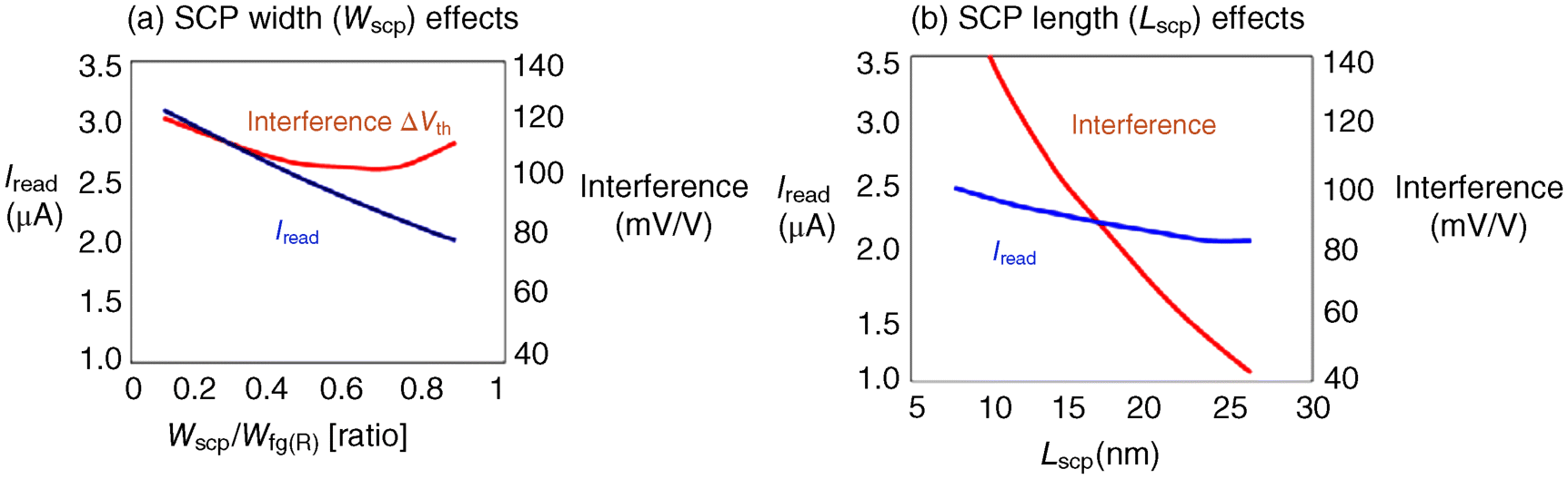
Figure 4.49 (a) SCP width (Wscp) effects on Iread and interference; (b) Iread and interference ΔVth dependence on SCP length (Lscp). (Based on M.S. Seo et al., (Tohoku University, Hynix), IMW, 20 May 2012 [32].)
Two types of interference effects were found: conventional indirect coupling between FGs and direct coupling from FG to SCP. As the ratio of Wscp to Wfg is increased, the indirect coupling effect was suppressed, but the direct coupling effect became more critical due to the influence of the channel potential in the SCP. As a result the interference effect of the cell was minimized at the 60% ratio of Wscp and Wfg. If the Wfg was decreased, the interference effect improved due to suppression of the coupling capacitance with the neighboring FG, and the Iread also improved. To evaluate the characteristics of the cell, 3D cylindrical device simulations were performed vertically on the eight-cell NAND string. The geometric effects of the cell were confirmed. The FG NAND flash memory cell operation using the SCP was shown using simulation to have good scalability and cell performance. The potential for MLC operation was shown to have sufficient interference margin and good reliability characteristics.
The basic cell size of the SCP NAND FG cell is about 60% larger than that of the CT NAND cell. If a 2-bit MLC is used, then the effective cell size of the SCP FG NAND cell is about the same size as a CT NAND cell. A 3-bit MLC could also be used with correspondingly smaller effective cell size.
4.3.5 Trap Characterization in 3D Vertical Channel NAND Flash
A characterization of traps in a 3D vertical channel NAND flash was discussed in December of 2012 by Seoul National University and Hynix [33]. Trap density was extracted in this 3D VC flash. The trap density extracted by the conductance method was 1–2 × 1012 cm−2 eV−1 in Ec–Et of 0.15–0.35 eV. Simulation results were compatible with the measurements. The effects of P/E cycling stress on 1/f noise was also studied, and the position was defined as a trap-generating RTN by considering cylindrical coordinates and pass cell resistance in the 3D stacked NAND flash cell. The traps of grain boundaries in vertical polysilicon channels are of interest for characterization because these traps can induce high leakage degradation of the subthreshold swing and degrade mobility. RTN can cause fluctuations in the read current. This study involved the characterization of traps due to the polysilicon grain boundary and characterization of the RTN.
The 3D stacked NAND flash had a vertical polysilicon body, gate dielectric stack with Si3N4 layer and a virtual S/D. The cell string was similar to that of the p-BiCS structure. Gate length, space between vertical WLs, and tube diameter are less than 100 nm. Normalized noise power of the 3D stack devices was analyzed, and a method to extract a trap-generating RTN was developed and verified [33].
4.3.6 Program Disturb Characteristics of 3D Vertical NAND Flash
Program disturbance characteristics of 3D vertical NAND flash cell arrays were discussed in May of 2013 by Hynix [34]. Program disturbance in both the X and Y directions are considered. Characteristics are compared with 2D planar NAND flash cells. A new program method for 3D NAND flash was proposed to determine the disturbance characteristics for MLC NAND flash arrays.
Most 3D NAND flash cells have adopted an undoped or uniformly n-doped polysilicon channel, which makes the subthreshold swing of the select transistor worse than in the case of 2D NAND flash using single-crystal silicon. In addition, the number of strings per block is increased over that of 2D NAND flash, which increases the “number of program” stresses. There is a new program disturb mode that is worse than conventional program disturb. While there is only an x program disturbance in 2D NAND flash, an unselected string in 3D NAND flash has potential program disturb on axis x, y, and xy, as illustrated in Figure 4.50 [34].
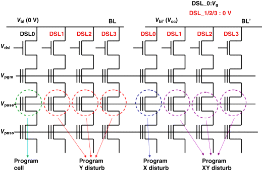
Figure 4.50 3D NAND flash cell program disturb mode. (Based on K.S. Shim et al., (Hynix), IMW, 20 May 2013 [34].)
Each mode has a different backbias level of drain selection line (DSL) transistor, with each Vbl and Vdsl. Program Y disturbance mode has the lowest backbias level, and so can expect the worst cutoff characteristics. Program X disturbance is defined at Vbl = Vcc and Vdsl, which is the condition for a conventional 2D planar NAND flash cell. Program XY disturbance has a higher DSL backbias level than the 2D case, which means a smaller disturbance Vth shift than the other modes. The select transistor with the poly channel shows worse swing characteristics than the 2D select transistor with single-crystal silicon, so the select transistor cutoff characteristics in program disturb mode are worse for a 3D vertical cell than a 2D planar cell [34].
To improve the inherent program disturbance of a 3D cell, a high DSL Vth compared to 2D should be used to suppress the leakage current. DSL vias of the selected BL during programming should also be increased by the same amount to prevent slow programming. In the 3D cell structure DSL Vth can be controlled by channel Vth implant. However, the vertical channel topology could add extra nonuniformity to the DSL Vth, unless process control for uniform cell topology is maintained. In addition, negative Vdsl needs to be applied to improve cutoff characteristics in program Y disturb mode. If high negative Vdsl is applied, GIDL current could be increased in the overlap region between the DSL transistor and the boosting channel and could make the boosting level lower. This means there is an optimum negative DSL bias. Finally, the edge WL's program disturb characteristics are much worse than those of other WLs. Because a 3D cell has a floating body structure, the SSL channel potential is raised by the program bias of the edge WL during program. The channel boosting level of the edge WL becomes lower than other WLs by the DIBL current, and dummy WLs are needed between the select transistors and main WLs to prevent DIBL current [34].
4.4 3D Stacked NAND Flash with Lateral BL Layers and Vertical Gate
4.4.1 Introduction to Horizontal BL and Vertical Gate NAND Flash
3D stacked NAND flash with layered horizontal BLs and vertical gates is an alternative structure to vertical BL pipes with through-holes in which tunneling oxide, polysilicon body, and blocking dielectric are formed sequentially. An attribute of the stacked horizontal BL architecture is that this is the orientation of the BLs in the conventional planar NAND flash.
Issues for vertical pipe structures include a limitation in the number of vertical bit cells and in the large Vth distribution in a BL because the through-hole diameter becomes narrower at the bottom as the number of cells increase. Another issue with vertical pipe devices is that metal gate structures tend to have poor retention characteristics during high-temperature operation from stress due to the high thermal expansion coefficient. It is possible that a stacked structure will eliminate some of these issues. Vertical pipe structures also have a pitch scaling issue, which makes a 4F2 cell a difficult proposition. Vertical gate architectures do not have the pitch scaling issue, so a 4F2 cell is possible; however, the cell select/decode is more difficult.
3D TCAD simulations on various 3D NAND flash memory architectures, including the vertical channel P-BiCS, TCAT, and VSAT as well as the horizontal channel vertical gate memory, were discussed by Macronix in May of 2010 [2]. All structures have an X,Y lateral scaling limitation due to the minimal 20 nm ONO thickness and 10 nm poly channel thickness that can not be scaled further. The characteristics of these technologies are summarized in Table 4.4 [2].
Table 4.4 Characteristics of Various 3D NAND Flash Technologies.
| P-BICS | TCAT | VSAT | VG | |
| Device Structure | GAA | GAA | Planar | Double gate |
| Cell Size (xy plane) | >4F2 | >4F2 | >4F2 | 4F2 |
| Gate Process | Gate first | Gate last | Gate first | Gate last |
| Direction of Current | Vertical | Vertical | Mixed | Horizontal |
| Based on Y. H. Hsiao et al., (Macronix), IEEE IMW, 16 May 2010 [2]. | ||||
Of these architectures, the vertical gate memory was found to have the better X-direction scalability and no penalty for increasing the number of layers in the vertical Z direction because the channel current flows horizontally. Simulations showed that a buried-channel junction-free NAND improved the read current for all 3D NAND arrays. In the vertical pipe structures, NAND string read current was shown to decrease with increasing vertical layers because the string length was being increased. The read current in the vertical gate structures was independent of Z layer number because each layer was independent. A vertical gate stacked NAND flash with horizontal BLs is possible with GAA as well as double-gate structures. Interference in the Z direction was also examined, and both vertical channel and vertical gate memories were shown to suffer from it. A new Z-direction scaling limitation was indicated [2].
4.4.2 A 3D Vertical Gate NAND Flash Process and Device Considerations
A 3D stacked NAND flash memory with lateral BL layers and vertical gates was discussed in June of 2012 by Seoul National University [35]. A schematic view of the process sequence for fabricating a 3D stacked NAND flash memory device is shown in Figure 4.51.

Figure 4.51 Schematic process sequence of a 3D stacked NAND flash memory. (Based on J.W. Lee et al., (Seoul National University), Silicon Nanoelectronics Workshop, 10 June 2012 [35].)
The fabrication sequence consisted of depositing 40 nm of SiO2 and 100 nm of polysilicon alternately on the silicon substrate followed by boron ion implantation doping with three different energies to dope the three polysilicon layers. The trench was formed using dry etching with a hardmask for active layers. The three stacked layers of polysilicon form BLs, which were separated by SiO2. The side of the polysilicon was used as a channel. A tunneling oxide–nitride–blocking oxide (ONO) stack was formed by consecutive deposition. After the ONO was formed, a doped polysilicon was deposited for the WL and to fill the trench. The doped polysilicon was then etched to pattern the WLs. The side n+ regions were then formed by ion implant except in the regions overlapped by the WLs. To form the n+ regions, arsenic ions were implanted, tilted by 30 degrees with two rotations, forming the n+ regions on the sides of the etched polysilicon layers.
Anneal of the implanted ions was then done. The blocking oxide and nitride layers between WLs were then selectively removed using a wet etch to separate the CT layers. Contact holes at the bottom and center BLs were formed by etching the top BL layer first and then the center BL near the contact holes for the bottom BL. n+ doping was done at both ends of the BL body to give contact regions for BL wiring. A layer of oxide was deposited, and contact holes were etched. The metal stack Ti–TiN–Al–TiN was sputtered and etched for a metal pad.
The P/E characteristics are shown in Figure 4.52 [35]. This shows the BL current vs. CG bias of the 3D stacked NAND flash. 19 V was used for programming and −18 V for erase. The ΔVth was 2.4 V when the BL current (Ibl) was 10 nA. Because the channel was formed on the side of the etched polysilicon body, the device characteristics suffered.
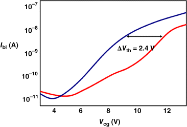
Figure 4.52 BL current vs. control gate bias of the 3D stacked NAND flash. (Based on J.W. Lee et al., (Seoul National University), Silicon Nanoelectronics Workshop, 10 June 2012 [35].)
Retention characteristics showed minimal charge loss up to 104 s. The Vth for the programmed state tended to decrease from 2.44 V initially to 2.1 V after 104 s and to 1.84 V after 106 s. For endurance, the shift in Vth was 1.58 V after 104 cycles. To improve the quality of the side channel, a chemical dry etch was used after etching the BL stack to remove etch damage. As a result the current–voltage characteristics improved slightly.
The effect of variation on the vertical profile of gate dimensions in 3D stacked NAND flash with multiple stacked layers was discussed in June of 2012 by Seoul National University [36]. In 3D stacked NAND flash, the number of stacked layers increases to increase the memory capacity of the storage. If the height of the stacked array is increased, it becomes more important to have a good vertical etch profile because WL gate dimensions are affected.
The effect of variation of gate dimensions on the program characteristics in 3D NAND flash was investigated using a TCAD simulation. The cell characteristics with different 3D structures were compared, including GAA and double-gate CT NAND flash memory. A 3D stacked NAND flash memory is illustrated in Figure 4.53 [36].

Figure 4.53 3D schematic of 3D stacked NAND flash memory. (Based on J.Y. Seo et al., (Seoul National University), Silicon Nanoelectronics Workshop, 10 June 2012 [36].)
In an array with multiple stacked layers, a slight deviation from 90 degrees on the etch slope resulted in a significant change of the dimensions between the gates on different layers. This study reported how the dimensions of the gates, in particular the Lg, affect the program characteristics in 3D NAND flash arrays. The change in the gap in double-gate and GAA structures on different layers is illustrated in Figure 4.54 [36].

Figure 4.54 Schematic illustration of a (a) double-gate; and (b) GAA structure. (Based on J.Y. Seo et al., (Seoul National University), Silicon Nanoelectronics Workshop, 10 June 2012 [36].)
With the GAA structure, the variation of Lg did not appear to affect the current-voltage characteristics initially. The level of BL current remained constant. This meant the program characteristics of the GAA structure were not changed by variation of Lgap whether the gate length was 40 nm or 70 nm.
For the double-gate structure, however, the cell characteristics were subject to a change in the gate dimension. When Lg was less than 50 nm, the program characteristics could not be determined. There was a reduction in the level of BL current as Lg decreased. This was because the fringing field was not sufficient to induce the inversion layer between gates as the distance between gates got longer. This led to low electron density in the virtual S/D area. The result was that the double-gate NAND flash cells located in the upper layer could not guarantee stable program characteristics. To guarantee stable cell characteristics, the gap between WL gates had to be smaller than 50 nm. It was found that the maximum height of total stacked layers for the double-gate NAND as a function of the etch slope was the equal to height when the WL gap is 50 nm at the top of the gates and 10 nm at the bottom of the gates.
The conclusion was that the etch slope limits the total height of the stacked layer when double-gate NAND architectures were used. In addition, the NAND flash memory cells with GAA architecture were less sensitive to variation of the gate dimensions than cells featuring a double-gate structure. The GAA architecture appeared to be more suitable for very high-density NAND flash memory cells.
4.4.3 Vertical Gate NAND Flash Integration with Eight Active Layers
The integration of a vertical gate NAND flash array with multiple (eight) active layers was discussed in June of 2009 by Samsung [37]. Stable operation of program, erase, and read was confirmed. There was no accumulation of program disturb with increased numbers of vertical layers due to the vertical block architecture. A top view of the 4F2 cell is shown in Figure 4.55 [37].
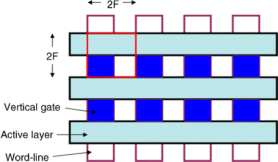
Figure 4.55 Top view of vertical gate NAND flash with multiple active layers. (Based on W.J. Kim et al., Samsung, VLSI Technology Symposium, June 2009 [37].)
One of the issues that vertical NAND flash strings had was increased program disturb and channel resistance as the number of WLs between top BL and bottom CSL increased. In this study, vertical gates and horizontal multiple active layers were introduced to solve some of these issues [37].
The formation of the vertical gate NAND used the following sequence:
- The source line, BL, and CSL were formed.
- Then multiple active layers (ONO) were deposited with ion implants and active patterning.
- The CT layer was deposited over the patterned active layers.
- The vertical gates were formed.
- Vertical plugs of drain current (DC), source, and body bias (VBB) were plugged [37].
Multiple SSL's were used to select data from a chosen layer out of multiple layers because the vertical gate NAND used common BL and common WL between multiple active layers. The number of process steps for the vertical gate NAND with multiple active layers was comparable to the one for planar NAND. P/E cycling to 1000 cycles and retention to 109 s were confirmed. A sketch of the cross-section of the vertical gate NAND along the WL direction is illustrated in Figure 4.56, which shows the eight active layers and the vertical gates [37].

Figure 4.56 Sketch of a SEM of the cross-section of vertical gate NAND along word-line direction. (Based on W.J. Kim et al., (Samsung), VLSI Technology Symposium, June 2009 [37].)
A schematic circuit diagram of the vertical gate NAND array is shown in Figure 4.57 [37]. NAND strings were horizontal in eight layers. WLs and gates were vertical. Source and body were tied to CSL. Each BL contained multiple active strings, a common vertical gate, and vertical plugs.
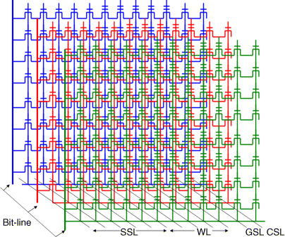
Figure 4.57 Schematic circuit diagram of eight-layer vertical gate NAND array. (Based on W.J. Kim et al., (Samsung), VLSI Technology Symposium, June 2009 [37].)
Program and body erase were done, and a 3.7 V program window resulted. The channel of the selected layer was boosted with a channel precharge, while channels of the nonselected layers were boosted without channel precharge during program inhibit operation. No distinguishable difference in program disturbance was found between the channel with and without precharge when there was a program window of 2.8 V. P/E endurance up to 1000 cycles was found.
A vertical block strategy was implemented for the vertical gate NAND, which reduced program disturbance because each vertical block used its own WL during program operation. Factors considered to cause complications in vertical channel NAND devices included number of trimmed WL contacts, program disturbance, and channel resistance due to increasing numbers of WLs between the BL and CSL. The channel resistance of both vertical channel NAND and vertical gate NAND was expected to increase with the number of layers at about the same rate. The number of WL contacts and the PGM disturbance were expected to be significantly different and are shown in Figure 4.58, which illustrates this advantage of the vertical gate NAND over the vertical channel NAND. The factor x1 is based on planar NAND with 32 WLs [37].
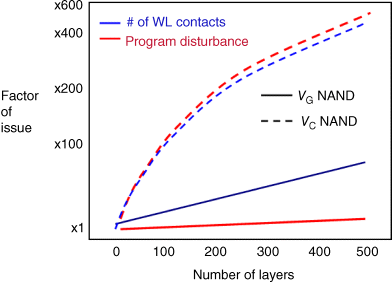
Figure 4.58 Advantages of vertical gate NAND over vertical channel NAND in program disturbance. (Based on W.J. Kim et al., (Samsung), VLSI Technology Symposium, June 2009 [37].)
4.4.4 3D Stacked CT TFT Bandgap-Engineered SONOS NAND Flash Memory
An eight-layer 3D vertical gate TFT bandgap-engineered (BE) CT NAND flash was discussed in June of 2010 by Macronix [38]. A buried channel n-type well device was used to improve the read current of TFT NAND. The buried channel permitted a junction-free structure, which is important for 3D stackable devices. A 6 V disturb-free memory window was achieved. The Z interference between adjacent vertical layers was studied [38].
A 3D array architecture of the vertical gate CT BE-SONOS is shown in Figure 4.59 [38]. The layout resembled the conventional NAND. The WLs were in the vertical plane, and the BLs were in the horizontal plane. Array efficiency is similar to that of the conventional NAND. An n-type depletion mode buried channel was used. The BE CT technology was discussed in Chapter 2 [38].

Figure 4.59 3D array architecture of vertical gate charge-trapping BE-SONOS. (Based on H.T. Lue et al., (Macronix), VLSI Technology Symposium, June 2010 [38].)
Each cell was a double-gate junctionless TFT BE CT device. A schematic cross-section of the BL in the X direction showing the BE CT device is shown in Figure 4.60 [38]. It shows the p-poly gate, the n-type polysilicon buried channel, and the BE-SONOS layer structure including the ONONO. The poly channel thickness was about 18 nm. The half-pitch of the structure was 75 nm technology.

Figure 4.60 Schematic cross-section of p-poly gate and BE-SONOS memory structure. (Based on H.T. Lue et al., (Macronix), VLSI Technology Symposium, June 2010 [38].)
A proposed scaling to a half-pitch of 25 nm in both the X and Y directions was proposed. This resulted in a vertical pitch of 60 nm, an ONO of 5 nm, 6 nm, and 6 nm, respectively, and a Vpass of 7 V. Array characteristics were determined. The read current of a 32-WL TFT NAND array was determined for various channel dopings. The buried-channel n-type well device showed improved read current over the surface channel p-type. A > 7 V memory window was found. The FN erase is different from the conventional substrate erase due to the floating body cell. In this case the BLs and source lines are raised together to provide an efficient FN erase on each WL.
Self-boosting programming was used for array operation with Vpgm applied to cell A while neighboring cells B, C, D, and E remained in the erased state. Cell A was the programmed cell with the corresponding BL and source line grounded. In all three dimensions, neighboring cells B, C, D, and E were inhibited. Figure 4.61 shows that during programming of cell A, the neighboring cells could be sufficiently inhibited [38]. The disturb-free window was nearly 6 V. Due to the junction-free channel and the floating body structure, the channel potential was mainly boosted by the Vpgm.

Figure 4.61 Programming cell “A” by self-boosting with neighboring cells in 3D inhibited. (Based on H.T. Lue et al., (Macronix), VLSI Technology Symposium, June 2010 [38].)
Z interference that comes from the fringing field induced potential change due to the floating body. It depended on the thickness of the buried oxide between adjacent layers. When the buried oxide thickness was greater than 40 nm, the Z interference was smaller than 200 mV when cell A was programmed with a 4 V Vth shift.
The various layers showed equally good endurance. Because the vertical gate NAND array was a “gate-last” process, there was no tunnel oxide damage. After 104 P/E cycles, the Vth window remained at about 4 V. Program was at 20 V for 200 μs and erase was at −13 V for 100 ms. Retention, after 150 °C bake for 105 s, retained a Vth window of about 4 V.
4.4.5 Horizontal Channel Vertical Gate 3D NAND Flash with PN Diode Decoding
In June of 2011 Macronix discussed a vertical gate 3D NAND architecture with p-type silicon n-type silicon junction (PN) diodes self-aligned at the source side of the vertical gate [39]. The BE-SONOS junctionless cell technology was used. A PN diode decoding method eliminated the need to make multiple SSL transistors inside the array, which enabled a symmetrical, scalable array structure as shown in Figure 4.62 [39]. A three-step programming pulse waveform was used to implement the program-inhibit method of programming. This method took into account the fact that the PN diodes could prevent leakage of the self-boosted channel potential. A greater than 5 V disturb-free program window was shown.

Figure 4.62 Vertical gate 3D NAND with self-aligned PN diodes. (Based on C.H. Hung et al., (Macronix), VLSI Technology Symposium, June 2011 [39].)
Vertical gate architectures do not have the pitch-scaling issue that the vertical channel architectures have, so a 4F2 cell is possible. However, the cell select/decode is more difficult. The solution proposed here was PN diode decoding, which eliminated the need to make multiple SSL gates in one block and resulted in a simple, scalable array.
For PN diode decoding, PN diodes were formed at the source side of the vertical gate NAND. The ON–OFF ratio of the diode was greater than six orders of magnitude, and the reverse current had leakage below 10 pA. Source lines of each memory layer were separately decoded, while WL, BL, SSL, and GSL were common vertically for the multilayer stacks. There was only one SSL and one GSL per block. A three-step programming pulse waveform was used to implement the program inhibit technique. This method used the PN diodes to prevent leakage of the self-boosted channel potential. A greater than 5 V Vth window was found free of program disturb. The PN diode decoding technique resulted in robust program disturb immunity without using a complex SSL design, and it had scalable pitch.
4.4.6 3D Vertical Gate BE-SONOS NAND Program Inhibit with Multiple Island Gate Decoding
In May of 2012, Macronix studied the program inhibit performance of their 3D vertical gate NAND flash, which uses a multiple island gate SSL decode. In this architecture, the array efficiency is improved by sharing WLs in the vertical direction and BLs in the lateral direction, as shown in Figure 4.63 [40].

Figure 4.63 3D vertical gate NAND flash with multiple island gate SSL decode. (Based on K.P. Chang et al., (Macronix), IMW, 20 May 2012 [40].)
For correct decoding of the array, every channel BL had its own island gate SSL control device. Many channel BLs were grouped together in one unit, and staircase BL contacts were formed to decode the various memory layers. A page operation occurred naturally by selecting each island gate SSL device. Due to the multiple SSL devices, the architecture had more pages when the number of stacked layers increased. This meant that program inhibit stress was larger than in conventional 2D NAND.
A top-view schematic diagram of the 3D vertical gate NAND with WLs of the vertical layers shared is shown in Figure 4.64 [40]. Every horizontal channel BL was separately decoded by one vertical island gate SSL device. In one unit that contained 2 × N (where N is the number of layers) channel BLs, all BLs were grouped together for each layer and connected to the metal layer 3 (ML3) BLs through the staircase BL contacts formed at the BL pad region. All island gate SSL devices were connected by CONT/ML1/VIA1/ML2 routing toward the SSL decoder. A CSL was used to share the source lines of all memory layers.

Figure 4.64 Top-view schematic of 3D vertical gate NAND with word-lines of the vertical layers shared. (K.P. Chang et al., (Macronix), IMW, 20 May 2012 [40], with permission of IEEE.)
Looking from the top down, the 2D layout schematic in Figure 4.64 is for N = 4 stacks. Every 2 × N = 8 channel BLs are grouped into one unit that share the same BL pad. In the BL pad, a staircase contact is made where each contact corresponds to one memory layer. The staircase contact is connected by ML3 BLs toward the page buffer for memory sensing. Each channel BL has its own island gate SSL for selection. The SSLs are connected through CONT/ML1/VIA1/ML2 toward the SSL decoder. A common source is made to connect source lines of all memory layers. Each device is a double-gate TFT BE-SONOS device and is selected by the intercept of the WL (Y direction) the ML3 BL (Z direction) and the SSL (x direction).The chip has 16Kb BLs and four memory layers. Because the ML3 BL has double X pitch, the total number of ML3 BL is 16Kbit/2 or 8 Kb, and the total unit number is 2Kb. Every unit has eight pages, where each page is defined by the selection of one SSL. To select one page for each WL, a total of 2Kb SSL devices is selected in many parallel units. For all-BL sensing for the four layers, the total number of selected devices are 2Kb × 4 or 8 Kb, which defines the page size [40].
To study the program disturb property during page operation, a two-layer device was made. It was found that the program disturb stress increased linearly as the number of memory layers increased, due to the greater number of pages. Program disturb testing results projected that the device had program disturb immunity sufficient to support more than 32 stacked memory layers.
4.4.7 3D Vertical Gate NAND Flash BL Decoding and Page Operation
The BL decoding and page operation of a 37.5 nm half-pitch 3D BE-SONOS NAND flash with 16 stacking layers was discussed in June of 2012 by Macronix [41]. This array was expected to be cost competitive with a 20 nm 2D NAND flash. A 3D vertical gate NAND was shown using a self-aligned IDG SSL transistor method of decoding. The IDG SSL improved program inhibit and read selection without increasing the cell size.
The decoding method was more difficult for vertical gate devices than for vertical channel ones because the BLs were horizontal and difficult to decode. The decoding method affected the design of the page operation as well as the cell size and array overhead.
This study proposed a self-aligned IDG SSL decoding technique for 3D vertical gate NAND. A 30 nm node range half-pitch 3D NAND was demonstrated, and good program inhibit performance was shown. A schematic of the IDG decoded 3D vertical gate NAND flash array structure is shown in Figure 4.65 [41]. The memory was a double-gate TFT CT device made by the intercept of source lines and BLs. The intercepts of the WL and BL can be seen in the upper structure. The BL contacts formed a staircase with the various memory layers, connecting the corresponding BLs to ML3. The SSLs were divided into a poly gate between the channel BLs and connected through ML1 and ML2 to the SSL decoder. A CSL was made that connects all source lines of every memory layer.
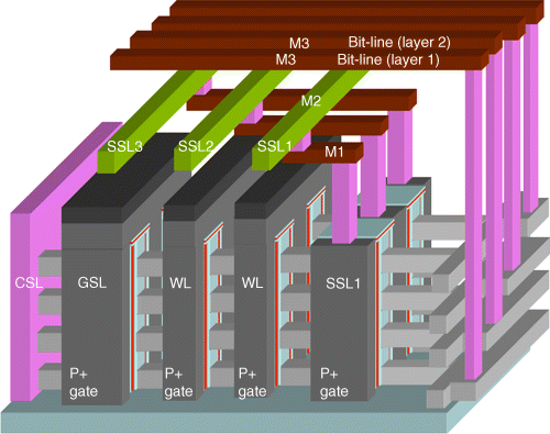
Figure 4.65 Schematic of IDG decoded 3D vertical gate NAND flash array structure. (Based on C.P. Chen et al., (Macronix), VLSI Technology Symposium, June 2012 [41], with permission of Macronix.)
The IDG decoded 3D vertical gate had a layout similar to that of a conventional NAND. It did not require additional area because it was self-aligned and the pitch was scalable. A top-down view of the layout schematic of the IDG decoded array is shown in Figure 4.66 [41]. This was an eight- layer stack. It had conventional WLs and BLs with SSLs divided into 16 groups that corresponded to 16 pages for each WL. The SSLs were connected through ML1 and ML2 to the SSL decoder. The BL pad in each unit shares 2N (16 = 2 × 8 layers) channel BLs. Every unit had N(8) different BL contacts that corresponded to various memory layers. When the number of memory stacks was increased, the layer efficiency remained unchanged but the page number of each unit and the BL pad layout did change.

Figure 4.66 Top-down view of layout schematic of ICG decoded array. (C.P. Chen et al., (Macronix), VLSI Technology Symposium, June 2012 [41], with permission of IEEE.)
Each memory device was selected by a WL, an ML3 BL, and the page that corresponded to the sandwich of two SSLs. Unselected adjacent pages were inhibited by the IDG SSL operation through the use of an inhibit bias on the other SSL gate. For the IDG SSL operation, a turn-on voltage Vssl = +2 V was applied to the two SSLs that sandwiched the selected channel BL. The adjacent unselected channel BL shared one side of the SSL, so a negative inhibit bias Vinhibit = −7 V had to be applied to the other side of the IDG SSL to turn it off [41].
The Id–Vg characteristics of the 30 nm range vertical gate TFT device showed good subthreshold behavior, which was due to good gate control capability in a narrow-width double-gate device. The Idsat of the array was over 150 nA, which gave sufficient current for memory sensing. The memory window was still well separated after program disturb stressing.
4.4.8 An Eight-Layer Vertical Gate 3D NAND Architecture with Split-Page BL
An eight-layer 3D horizontal channel stacked TFT NAND flash using BE CT devices with 64-WL NAND string with 63% array core efficiency was discussed in December of 2012 by Macronix [42]. The process had a WL half-pitch of 37.5 nm and a BL half-pitch of 75 nm. It was thought that an eight-layer stack device with this pitch could provide a technology at a lower cost than a conventional sub–20 nm 2D planar NAND. It was expected that this technique would permit NAND flash scaling below 15 nm node.
This architecture had two key features: the first was a split-page layout, with even and odd BLs and pages twisted in the opposite direction. This permitted island-gate SSL devices. The other key feature was a BL contact method that minimized the number of process steps. Metal interconnections were laid out in double pitch, which created a larger process window for BL pitch scaling. The 3D vertical gate architecture used WL and BL patterning so that the lateral pitch could be scaled in a similar manner to the 2D NAND. The decoding method for 3D NAND was, however, more difficult than for the vertical channel NAND; the BLs were horizontal and parallel to the multilayers and could, therefore, not be simply connected to metal BLs, as could be done with 2D NAND.
The vertical gate architecture used many rows of normally-on SSL devices to decode the BLs within the NAND string. As the stacked layer increased, the required number of rows of SSLs increased, which reduced the array efficiency. To compensate for this, an island gate SSL device was proposed in order to separate channel BLs for decoding. This permitted the array efficiency to be constant as the stack layers increased. However, making the island gate SSL within each channel BL was difficult with scaled BL pitch.
To improve scalability, a new architecture with a twisted layout was proposed in this study.
NAND strings were divided into even and odd pages so that string current flowed in opposite directions. This permitted the island gate SSL to be laid out at double the pitch of the BL. A top view of this split-page vertical gate architecture is shown in Figure 4.67 [42]. The island gate SSL devices were split into even and odd pages, and GSLs also had even and odd pages in the opposite direction, which provided a twisted BL layout. Each island gate SSL corresponded to one page during page program or read. In the BL direction, each BL pad grouped a total of 2 × N channel BLs, where each even or odd had N SSL devices per page. In the array, MI1 and MI2 connected the SSL gates to the decoder. Page operation selected one SSL in one unit and in parallel selected all units together. Staircase BL contacts in the BL pad connect to different memory layers. These contacts had double the pitch of the channel BL, which improved the process window. A poly plug was used for the staircase BL contact and source contact.

Figure 4.67 Top-down view of split-page vertical gate architecture. (S.H. Chen et al., (Macronix), IEDM, December 2012 [42], with permission of IEEE.)
A new method that used only three masks to define the contact for an eight-layer stack was implemented for the staircase contacts. This technique allowed 2M contacts using M masks. This staircase BL contact method of forming pages used the binary sum of M lithography and etching steps to achieve 2M contacts. This made it possible to minimize the number of etching steps by using multiple staircase contacts on each layer, which minimized the incremental layer cost. In this example three masks can be used to carry out eight-layer contacts; that is, random summation of 0,1,2,4 can generate 0,1,2,3,4,5,6,7. This means that to double the memory layer, just one more mask is needed. This is illustrated in Figure 4.68 [42].
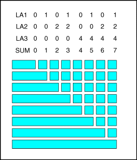
Figure 4.68 Minimal incremental layer cost method for staircase bit-line contacts. Random summation of 0,1,2, and 4 can make 0, 1, 2, 3, 4, 5, 6 and 7. To double the memory layer requires just one additional mask. (Based on S.H. Chen et al., (Macronix), IEDM, December 2012 [42].)
It was shown that each of the eight memory layers could be programmed with a memory window greater than 6 V. The schematic circuit diagram in Figure 4.69 shows the program inhibit method used for programming [42]. To program a page, the SSL for a page (page 0) was taken to Vcc while other SSLs had a slightly negative voltage applied to guarantee they were turned off. GSL (even) was turned off while GSL (odd) was turned on. Vcc was applied to CSL to inhibit. Page 2 (SSL2) was inhibited by floating the entire NAND string. Pages 1 and 3 were inhibited by precharging the channel using CSL and GSL.
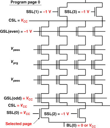
Figure 4.69 Schematic circuit showing program inhibit method for programming. (Based on S.H. Chen, et al., (Macronix), IEDM, December 2012 [42].)
Block erase used +13 V on CSL and BL, keeping all WLs at 0 V. A +6 V was applied to the SSL and GSL to reduce GIDL with minimum disturb to SSL and GSL. All memory layers and all WLs could be erased together. In this 3D vertical gate device, every WL had 2N pages, so to program one WL, every page had to endure a total number of program (NOP) stresses = 2N − 1. Stress capability was to sustain 64 = NOP stresses. The vertical gate NAND had planar ONO, which minimized the Vpass disturb. The conclusion was that an eight-layer 3D vertical gate NAND could provide a terrabit memory at 25 nm half-pitch using 32 stacked layers [42].
4.4.9 Various Innovations for 3D Stackable Vertical Gate
In December of 2012, Macronix discussed several design innovations for its 3D vertical gate NAND flash technology [43]. These included a “shift-BL scramble” intended to average the BL capacitances, which would provide uniform BL capacitances for various memory layers, optimized read waveforms intended to reduce the hot carrier–induced read disturb during page read, a reverse read with a multiple Vth sensing technique intended to compensate different memory layers for the Vth variation due to layer-to-layer process difference, and a program inhibit method for minimizing the Z-directional self-boosting program disturb present in 3D stacked memory. The result was improved chip performance with good memory window for SLC and MLC operations. This was demonstrated on a two-layer 3D vertical gate NAND chip.
An island gate SSL device was used to decode the array for different BLs. A scanning electron microscope (SEM) cross-section of the island gate SSL used to decode the array is shown in Figure 4.70 [43]. The CSL strapping area can be seen. In the CSL strapped area, the local ML1 CSL was connected toward the ML4 plate. A staircase BL contact was made and connected to the BL2 BL. ML1 and ML2 interconnects are used to decode the SSLs. An ML3 plate was used as the CSL to supply current during read [43].

Figure 4.70 3D schematic of two-layer device with island gate SSL device. (C.H. Hung et al., (Macronix), IEDM, December 2012 [43], with permission of IEEE.)
The 3D vertical gate stacked flash is considered the most pitch-scalable structure among all of the 3D NAND flash architectures. The decoding method is, however, more complex. To improve the decoding options, an island gate SSL was used to separate the BLs, and each memory layer was connected to its own metal BLs for sensing. The process window for the island gate SSLs was improved by splitting the even and odd pages to opposite sides of the array [43].
Each NAND string had 64 WLs connected in series with channel current flowing horizontally. The gate was shared vertically. Each memory cell was selected by the WL, BL M3, and SSL, which was an island gate SSL that separated the BL channel. In the BL direction, one unit had four (2 × N, where N = number of layers) pages, divided as even and odd pairs located on opposite sides. Each BL pad grouped 2 (= N) channel BLs in one side. Staircase BL contacts were made at the BL pad. The ML3 BL was connected to the page buffer for sensing the NAND string. ML1 and ML2 were used to connect SSL devices and the decoder. For page read and write, many SSLs from different units were selected together for high throughput. Four metal layers were used. M4 was the global CSL supporting a large current during page read [43].
The two-layer device was a 512Mb MLC test chip with core memory area of 2.3 mm ×2.6 mm. This area included the page buffer, WL, and SSL decoder and driver. Page size was 512 Bytes. More layers could be stacked with this configuration. The stack height of the array was significantly higher than those of the peripheral CMOS devices, which made planarization difficult. For this reason, the 3D vertical gate array was put in a deep trench in the silicon surface, and the peripheral CMOS devices were made on the original silicon surface, as shown in the schematic cross-section in Figure 4.71 [43].

Figure 4.71 Schematic cross-section of 512Mb MCL test chip process. (Based on C.H. Hung et al., (Macronix), IEDM, December 2012 [43].)
This CMOS-last process had the advantage of avoiding thermal budget issues on the peripheral CMOS. As a result, the periphery had similar characteristics to those of a 2D array and also had a high thermal budget, which could improve characteristics of the polysilicon TFT devices and optimize the ONO in the BE-SONOS.
An issue was that the ML3 global BL was connected to the different memory layers in each unit. Because of the parasitic capacitance of the BL pad, the capacitance was different for each layer. This led to about a 10% layer-to-layer capacitive difference. This effect was averaged out by using a “shift-BL scramble” design in which each ML3 BL was connected to different memory layers in various blocks. This technique provided a uniform BL capacitance for voltage sensing.
Another issue was optimizing the read waveform to suppress hot carrier–induced read disturb. An example is shown in the schematic circuit diagram in Figure 4.72 [43]. In this 3D array, each WL has 2 × N pages. A page read is done by selecting SSL0 while turning off the unselected pages. Because SSL must be off prior to sensing, if the selected WL is negative, then local self-boosting between the selected WL and SSL is induced during WL setup for both selected and unselected pages. The boosted channel potential induces hot carrier injection after many read cycles. This is illustrated in the read-timing diagram in Figure 4.73 [43]. Because there are many pages sharing the same WL, this read disturb can be a serious issue.

Figure 4.72 Schematic circuit diagram illustrating suppression of hot-carrier-induced read disturb. (Based on C.H. Hung et al., (Macronix), IEDM, December 2012 [43].)
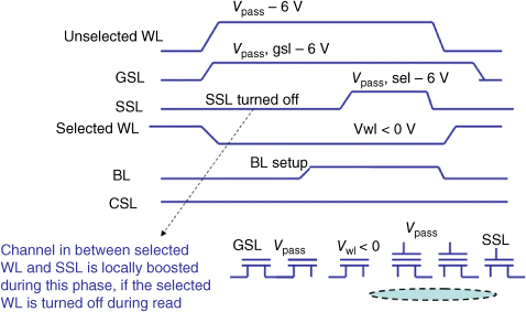
Figure 4.73 Read timing diagram of 3D vertical gate NAND flash showing read disturb. (Based on C.H. Hung, et al., (Macronix), IEDM, December 2012 [43].)
A solution for minimizing this read disturb is shown in the timing diagram in Figure 4.74 [43]. A “precharge channel to ground” was introduced at the rising phase of WL, while a “discharge channel to ground” was done at the falling phase. This avoided channel local self-boosting for both selected and unselected pages.
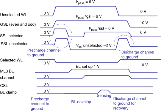
Figure 4.74 Timing diagram illustrating minimizing read disturb in 3D vertical gate NAND flash. (Based on C.H. Hung, et al., Macronix, IEDM, December 2012 [43].)
A layer-to-layer difference in the vertical slope of the etching process for the 3D NAND flash occurred. The bottom-layer device tended to be wider than the top-layer device and hence had a higher Vth and wider distribution due to the nonideal sloped BL profile. It was found possible to optimize the reverse read method so that the top- and bottom-layer Vth distribution could be tuned to being nearly the same.
A programming method was used to minimize Z-directional disturb. As an example, for page 0 programming, page 2 was inhibited by floating the NAND string without any precharging of the BL. Meanwhile, pages 1 and 3 were inhibited by precharging the CSL. A typical single-page checkerboard programming was used, where a large memory window of greater than 4.5 V was found within four pages of one WL.
Figure 4.75 shows the results of program disturb for a checkerboard when an adjacent memory layer was programmed [43]. Programming with and without Z-disturb showed Z-disturb causes about a 0.6 V higher Vth shift. The physical reason for the shift was that when adjacent vertical channels were at ground (i.e., programmed), the vertical capacitance coupling could reduce the boosted potential.

Figure 4.75 Program disturb with checkerboard pattern when adjacent memory layer is programmed. (Based on C.H. Hung, et al., (Macronix), IEDM, December 2012 [43].)
4.4.10 Variability Considerations in 2D Vertical Gate 3D NAND Flash
In December of 2012, Macronix discussed modeling the variability caused by random grain boundaries and the trap-induced asymmetrical read behavior for a vertical double gate 3D NAND TFT device [44]. A 37.5 nm half-pitch vertical gate NAND flash was made and characterized, and the random grain boundary effect was modeled using TCAD simulation. In the model used, the grain boundary created interface states that resulted in large local band bending and a surface potential barrier. Major physical mechanisms considered that affect the subthreshold behavior are gate-induced grain barrier lowering (GIGBL) and drain-induced grain barrier lowering (DIGBL).
Using the modeling, the impact of BL and WL critical dimensions of the double-gate TFT device were studied. It was found that narrower BL and larger WL critical dimensions were the most important parameters for providing tight Vth distribution and good memory window. An asymmetry was found of reverse read and forward read of the TFT device. This mechanism was explained using DIGBL. This asymmetry of reverse read and forward read could be used to determine the grain barrier trap lateral location and the interface trap density.
The polysilicon TFT device was needed to stack multilayer memory cells. Concerns in this case included large variability due to the random grain boundary traps and low mobility of the polysilicon channel. The variability of the TFT was the primary concern because an uncontrolled Vth distribution could cause the device to fail. This is particularly a concern with MLC devices. The low mobility was less critical because the large page size could compensate for a slower read latency. For this reason, the main focus of the study was on the variability model.
Each memory cell was a double-gate TFT BE CT device. A 37.5 mm half-pitch WL device was made. Critical WL dimension was 25 nm. A 64-transistor NAND string was used with an outer SSL–GSL select transistor. The critical dimension in the BL direction was about 30 nm. Several thermal annealing steps were done to increase the grain size and improve the polysilicon channel property. The channel was made of undoped polysilicon in order to reduce the doping fluctuation. The array was junction free with no N+ S/D. The fringe field of the adjacent pass gate bias induced a virtual inversion junction during read operation. The string Idsat was greater than 100 nA, which was sufficient for NAND sensing. It was found that narrower BL critical dimensions greatly improved the subthreshold slope behavior and gave a tighter Vth distribution. The transconductance and Idsat were not found degraded for narrower BLs because the inversion channel was induced primarily at the sidewall of the BL so that effective channel width was not proportional to the BL critical dimension [44].
It was estimated that the polysilicon grain sizes ranged between 20 and 50 nm. The TCAD simulation represented the grain boundary traps outside and beneath the selected gate. The subthreshold degradation and Vth for both cases were explored. In the case of grain boundary traps outside the selected gate, smaller degradation was found than for the fresh state. For traps beneath the gate, there was significant subthreshold degradation and higher Vth [44].
The impact of grain boundary traps in the TFT subthreshold current is shown in Figure 4.76 [44]. The insertion of grain boundaries lowers the surface potential and is the same as creating a higher surface potential barrier because the electron is negatively charged. It requires higher gate bias to reduce the barrier. In the example in Figure 4.76, the grain barrier was assumed to be at the gate center, where the barrier potential is lowered. Vg = 7 V was sufficient to reduce the barrier. This phenomenon is called GIGBL.

Figure 4.76 Impact of grain boundary traps in TFT subthreshold current. (Based on Y.H. Hsiao et al., (Macronix), IEDM, December 2012 [44].)
The drain bias also caused a drain-induced grain barrier lowering (DIGBL) effect, as shown in Figure 4.77, where the larger drain bias helped lower the grain boundary–induced surface potential barrier [44].
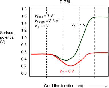
Figure 4.77 Illustration of DIGBL effect. (Based on Y.H. Hsiao, et al., Macronix, IEDM, December 2012 [44].)
The variability of 3D TFT NAND devices was accurately modeled using classical transport 3D TCAD with added grain boundary trap effects. The asymmetry of reverse and forward read was modeled, and a method for profiling the grain boundary trap lateral location and the interface trap density was suggested [44].
4.4.11 An Etching Technology for Vertical Multilayers for 3D Vertical Gate NAND Flash
An etching technology for preparation of smooth vertical multilayer stacked SiO2 and polysilicon BLs for use in 3D vertical gate NAND flash was discussed by Macronix in May of 2013 [45]. The shape evolution profile required was from tapered to less than 10 nm critical dimension difference between the bottom and top polysilicon layers. This ideal etch profile was done by an etch–trim–etch process sequence. A test chip was made with seven pairs of SiO2 and polysilicon layers. Initially, an organic antireflective film was deposited on top of the SiON. Photolithography followed using a 193 nm ArF scanner. The etch process consisted of various etch steps carried out using a commercial conductor etching chamber. A layer-to-layer etch sequence was then used; it consisted of etching the SiO2 and polysilicon layers separately, using different etching plasmas. The critical dimension difference between the eighth (top) polysilicon layer and the first (bottom) polysilicon layer was 42 nm and 77 nm, or a 35 nm difference. This was considered too tapered for use in a 3D vertical gate NAND flash cell. Electrical operation depends on the critical dimension difference between bottom and top polysilicon layers being less than 15 nm.
An etch sequence following the layer-to-layer etch was established. It consisted of an isotropic trim step and a high-energetic CFx ion bombardment etch step. The resulting critical dimension difference between the bottom and top polysilicon layers was less than 10 nm. The amorphous carbon hardmask was found sufficient even after the energetic bombardment step. The resulting profile was smooth and vertical within 10 nm top to bottom. An illustration of the initial film stack is shown in Figure 4.78 [45]. The stack consisted of seven layers of SiO2 alternated with polysilicon topped by a thick SiO2 layer and an amorphous carbon hardmask.

Figure 4.78 Smooth vertical multilayer stacked SiO2 and polysilicon bit-line stack. (Based on. Z. Yang et al., (Macronix), ASMC, 14 May 2013 [45].)
4.4.12 Interference, Disturb, and Programming Algorithms for MLC Vertical Gate NAND
In June of 2013, Macronix discussed MLC programming in 3D vertical gate NAND flash [46]. 2D FG NAND flash suffered from interference and disturb as the technology scaled, but much of the interference and disturb from scaling was alleviated in the 3D flash because the pitch was generally larger. The 3D NAND flash, however, suffered from a new source of disturb and interference as a result of operating in three dimensions.
A split-page 3D vertical gate NAND flash test chip was used to study the MLC programming algorithm. The memory array consisted of two layers of double-gate polysilicon TFT BE-SONOS CT devices. These devices had 37.5 nm half-pitch WL and a 64-WL NAND string. A 512Mb MLC test chip with 4Kb page size was used to develop the programming algorithms. Programming the split-page 3D vertical gate NAND architecture involved programming the pages. To program page 0, +Vcc was applied to SSL0 while other unselected SSLs were turned off. A BL pad was used to group several horizontal channels together. A staircase BL contact was made at the BL pad for memory layer decoding. For FN incremental step pulse programming (ISPP), the programming Vth distribution is an indicator of device intrinsic performance. Using polysilicon TFT device improvements, the intrinsic Vth sigma (standard deviation) was made smaller than 600 mV, and the distribution was uniformly shifted without erratic tail bits even after cycling. The advantage of a CT device being free of erratic tail bits was that it guaranteed there was no issue with overprogramming. This meant that the required ISPP bias range for various program-verify (PV) states could be estimated in order to minimize the number of programming cycles.
RTN is an intrinsic property of the device that limits the PV distribution. The PV distribution showed a finite Vth distribution that was consistent with the RTN distribution. WL and vertical (Z) interferences were found to be significant, but BL interference was found negligible because the poly gate shielded the adjacent BLs. Other diagonal interferences were also negligible. When two adjacent WLs in the same layer were programmed, WL interference contributed about a 400 mV Vth shift. The WL interference was caused by the junction-free NAND structure with tight-pitched WL because the adjacent pass-gate voltage affected the channel potential of the selected gate. The grain boundary interface trap could also make the WL interference worse. When the adjacent vertical layer was programmed, it showed about 150 mV Vth shift due to Z-directional interference. When adjacent vertical channels were programmed, the stored electrons changed the electrostatic potential of the selected channel. This “back-gate bias effect” was strongly affected by the Z-directional pitch. ONO, polysilicon, and buried-oxide thicknesses had to be optimized. These sources of interference came from electrostatic potential shift caused by the stored charge of an adjacent cell rather than from real charge injection in the selected cell. When there is real charge injection into the selected cell, it is called program disturb.
The primary program disturb mechanism in 3D vertical gate NAND was the Z-disturb. The Z-disturb occurred, for example, when the top poly layer was being programmed, the bottom poly layer was self-boosted, and the channel potential was raised. When both layers were boosted, there was a 600 MV smaller program disturb. Z-disturb-enhanced programming occurs when the second layer is also boosted, causing programming to be faster in the first layer. Z-disturb may introduce irregular programming speed when switching the programming code during PV. Vpass disturb requires a larger Vpass in order to increase the boosted channel potential. This in turn increases the Vpass disturb. In a 3D NAND flash, the many unselected pages normally introduce more Vpass disturb stress.
Programming algorithms were developed to reflect the understanding gained of the interference and disturb effects in the 3D vertical gate NAND device. A single ISPP sequence with reduced programming shots was developed that reflected the well-behaved ISPP Vth distribution, which had been found without tail bits. A layer-programming method was developed in which many layers were separated into three groups during programming. By doing this, each inhibited layer would only see one adjacent layer programmed so that Z-disturb was limited by one side only. In addition, each programmed layer always saw two adjacent layers boosted so the Z-disturb-enhanced programming was fixed during PV. Finally, the WL (WL) WL(n) was programmed to pre-PV, which was slightly smaller than the final PV. Programming WL(n + 1) would then introduce WL interference and raise WL(n)'s Vth slightly. Then WL(n) was programmed to the final PV. Iterating the pre-PV sequence would automatically compensate the WL interference. The optimized programming algorithms helped tighten the PV distribution. The wide memory window required less than 10 bits of ECC per page. The average number of page PV cycles was less than 40. It was believed that this made the device suitable for practical applications.
4.4.13 3D Vertical Gate NAND Flash Program and Read and Fail-Bit Detection
A 3D vertical gate NAND flash was discussed in June of 2013 by Macronix and National Tsing Hua University [47]. This device used circuit techniques to overcome degradations in speed, yield, and reliability that result from cross-layer process variations. These techniques included: layer-aware program, verify, and read (LAPV&R), layer-aware bitline precharge (LABP), and wave-propagation fail-bit-detection (WPFBD) schemes.
For LAPV&R, the profile of cells in a 3D vertical gate NAND array differ across layers because the etching processes do not produce perfectly vertical features. This affects program behavior, such as speed and Vth, and also creates disturb effects across layers. LAPV&R requires layer-aware Vth sensing to permit different Vth between layers and corresponding verify and read operations. The WPFBD scheme proposed takes only one cycle to detect a failed bit. For a design using j-bit error correction code (ECC), the detection cycle is repeated j times. For a 16Kb page with eight layers, WPFBD has a nine-times-faster fail-bit-detection (FBD) time than binary search FBD. A two-layer 3D vertical gate NAND test chip with 256Mb capacity was used to confirm that these various circuit techniques attain various target cell program Vth in each layer. They also need to attain a 40% reduction in sensing margin loss due to background pattern dependency with less than 0.1% area penalty for a gigabit-scale 3D vertical gate NAND device. The page size of the device was 512 bytes per page.
4.4.14 3D p-Channel Stackable NAND Flash with Band-to-Band Tunnel Programming
A p-channel 3D stackable NAND flash that uses new programming and erasing methods was discussed by Macronix in June of 2013 [48]. By using a p-channel 3D NAND, the disadvantage was avoided of GIDL-induced hole erase of the floating body n-channel NAND. This resulted in a very efficient FN hole erase and negligible disturb of the SSL and GSL devices. The p-channel NAND array permitted a new FN erase selection method. It also provided a new bit-alterable erase that allowed small-unit random code overwrite without block erase. In addition, the band-to-band tunneling–induced hot electron programming method provided lower operating voltage and enhanced scaling of the periphery. The device was implemented in a 37.5 nm half-pitch 3D vertical gate junction-free NAND architecture. A 3D schematic of the p-channel NAND array is shown in Figure 4.79 [48]. The memory device was junction free, while a P+ diffusion junction was formed at only one side of the long-channel SSL and GSL. The WL half-pitch was 37.5 nm, and the WL channel length was 25 nm.

Figure 4.79 3D schematic of p-channel vertical gate stacked NAND array. (Based on H.T. Lue et al., (Macronix), VLSI Technology Symposium, June 2013 [48].)
Most 3D NAND flash use n-channel devices in the array. A drawback of the use of an n-channel device was the need to use high +20 V FN programming bias so that the large CMOS WL drivers consume significant die area. For a negative FN block erase, GIDL-induced erase was needed. During a GIDL erase, a moderate negative voltage was applied to SSL and GSL, and a high positive voltage was applied to the BL and CSL to generate GIDL current at the SSL–GSL junction edge. Electrons and holes were generated by GIDL, and the holes were swept into the NAND string. The holes collected in the channel raised the channel potential, which led to negative FN hole-tunneling injection to the device. Drawbacks of GIDL erase include the following: the erase transient had time lag due to the long minority carrier (hole) generation time, and erase speed was dependent on GIDL current and SSL–GSL junction profile. Increasing GIDL current meant that higher negative voltages had to be applied to the SSL–GSL devices, which disturbed them during block erase. As a solution, this study proposed using a p-channel NAND with the lower-voltage hot electron programming. This permitted use of smaller CMOS design rules. GIDL erase was avoided in the p-channel NAND because channel hole erase could be easily induced without GIDL. The bit-alterable erase enabled a simple overwrite of any small unit without needing to use block erase.
In the p-channel 3D NAND architecture used, the TFT device had an undoped polysilicon channel and no junctions inside the NAND array. The P+ diffusion junction was formed only outside the long channel SSL and GSL devices. The junction-free NAND gave excellent short-channel device performance. The WL half-pitch was 37.5 nm with typical channel length of 25 nm. The NAND array used a 64-WL BL string. The device was a double-gate TFT BE CT device. The p-channel TFT NAND had similar read current to the n-channel device and had good subthreshold behavior. It was speculated that this result might mean that the hole mobility in a polysilicon TFT device was comparable to the electron mobility rather than slower, as found in a bulk device. Block erase was achieved using a high negative voltage applied to all WLs. Holes were easily induced in the p-channel NAND. While n-channel NAND often had an initial time lag for erase, there was no initial erase lag in p-channel 3D NAND, and the memory window was larger. The SSL–GSL had negligible disturb during erase.
For band-to-band hot electron programming, rather than using a large BL bias, local self-boosting was used to create a high virtual drain bias by channel boosting. A positive +9 V bias was applied to the selected WL(n) to cut off the p-channel NAND string, as shown in Figure 4.80 [48]. A large Vpass bias of −10 to −13 V was applied to WL(n + 1) and WL(63). The selected BL had Vcc = −3.3 V applied to boost the channel locally. A high band-to-band generation rate was found between WL(n) and WL(n + 1). Electron-hole pairs were generated by the band to band tunneling and accelerated by the lateral electric field, which induced hot carrier injection.
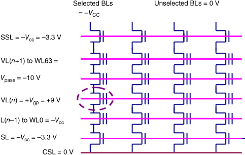
Figure 4.80 Band-to-band hot-electron programming method for p-channel 3D NAND. (Based on H.T. Lue et al., (Macronix), VLSI Technology Symposium, June 2013 [48].)
A large memory window with good inhibit was found. The programming was found to be more efficient with larger Vpass due to the larger boosted virtual drain bias. The Vpass stepping method was more efficient for programming and provided linear programming, with Vth linearly proportional to Vpass. When several pages shared the same WL, Vpass could be applied on unselected SSL. Because unselected SSL could not be turned off, self-boosting did occur. There was no hot hole injection observed for WLs with negative gate bias. This might mean that hot hole efficiency is weak in 3D TFT. Due to the need for a large Vpass, programming in sequence from G1 to G62 avoided having the negative Vpass disturb the already programmed cells.
For bit-alterable erase, the global self-boosting of the p-channel NAND could be done for negative FN erase select by inverting the bias polarity of the conventional n-channel NAND. This self-boosting erase technique showed good erase inhibit. The bit-alterable erase could also be performed in page mode to increase throughput.
An overwrite feature was available. When the device was already programmed by band-to-band hot electron injection, a bit erase on any small unit of the array could be performed without block erase. The operation bias in band-to-band hot electron injection and bit erase could be shifted simply by +Vcc so that negative voltage on the BL was avoided. It was possible to limit the maximum array operation voltage below an absolute 15 V, which permitted smaller CMOS design rules that could save area in the periphery.
4.4.15 A Bit-Alterable 3D NAND Flash with n-Channel and p-Channel NAND
A new bit-alterable dual-channel 3D NAND flash memory that had both n-channel and p-channel NAND characteristics was discussed in December of 2013 by Macronix [49]. The NAND channel was junction free with no dopant used inside the array. The drain side of the channel near the SSL was an N+ doped junction, while the source side of the channel near GSL was a P+ doped junction. A 3D schematic of an array with these characteristics is illustrated in Figure 4.81 [49].

Figure 4.81 Dual-channel 3D NAND with drain-side N+ bit-line and source-side P+ bit-lines. (Based on H.T. Lue, et al., (Macronix), IEDM, December 2013 [49].)
An advantage of this operation was that the carrier source for both positive FN programming and negative FN erase could be provided by either the N+ drain or the P+ source without waiting for the GIDL-generated minority carrier for the floating body 3D NAND. This resulted in faster FN speed than is possible with a conventional 3D NAND.
Both positive and negative FN operations had a suitable inhibit method, which enabled a bit-alterable flash memory. A positive pass-gate read voltage induced an n-type virtual S/D for the center WLs, which gave n-channel behavior. A negative pass-gate read voltage induced a p-type virtual S/D, which provided p-channel behavior. Id-Vg characteristics with very small leakage current resulted from both n-channel and p-channel reads.
For the array decoding method, a drain-side (N+) BL was vertically shared and connected to BLs in the metal one (M1) layer. On the source side (P+), the source line was horizontally shared and separately decoded for the various layers. The staircase source line contact was made every 128 ML1 BLs to reduce the source line loading. The source lines were then connected to the ML2 layer near the source line decoder. This array decoding method is illustrated in Figure 4.82 [49].

Figure 4.82 Array decoding method for the dual-channel vertical gate NAND flash. (Based on H.T. Lue et al., (Macronix), IEDM, December 2013 [49].)
The read method for the array consisted of applying +2 V to the selected source line while the unselected source line was set at 0 V. The selected BL was set at 0 V, while the unselected BL was set to +2 V. The source-side PN diode was necessary to prohibit the formation of a sneak path during read. The selected BL could be set at either 0 V or set slightly positive to obtain smaller background leakage. The typical polysilicon PN diode in the NAND array showed good on and off characteristics with small leakage and junction breakdown greater than 9 V.
The two sensing methods, both n-channel and p-channel read, were compared, and the trapped charge in the space between the WLs was identified. This both provided characterization of the lateral charge profile and also offered the potential for creating another storage node in the WL space inside the array.
References
- 1. Choi, J. and Seol, K.S. (June 2011) 3D Approaches for non-volatile memory, (Samsung). VLSI Technology Symposium.
- 2. Hsiao, Y.H., Lue, H.T., Hsu, T.H. et al. (16 May 2010) A critical examination of 3D stackable NAND flash memory architectures by simulation study of the scaling capability, (Macronix). IMW.
- 3. Tanaka, H. et al. (June 2007) Bitcost scalable technology with punch and plug process for ultra high density flash memory, (Toshiba). VLSI Technology Symposium.
- 4. Goda, A. and Parat, K. (December 2012) Scaling directions for 2Dand 3D NAND cells, (Micron). IEDM.
- 5. Clarke, P. (2013) Toshiba to Build Fab for 3D NAND Flash, EE Times (July 2).
- 6. Fukuzumi, Y. et al. (December 2007) Optimal integration and characteristics of vertical array devices for ultra-high density, bit-cost scalable flash memory, (Toshiba). IEDM.
- 7. Komori, Y. et al. (December 2008) Disturbless flash memory due to high boost efficiency on BiCS structure and optimal memory film stack for ultra high density storage device, (Toshiba). IEDM.
- 8. Maeda, T. et al. (June 2009) Multi-stacked 1G cell/layer pipe-shaped BiCS flash memory, (Toshiba). VLSI Circuits Symposium.
- 9. Katsumata, R. et al. (June 2009) Pipe-shaped BiCS flash memory with 16 stacked layers and multi-level-cell operation for ultra high density storage devices, (Toshiba). VLSI Technology Symposium.
- 10. Ishiduki, M. et al. (December 2009) Optimal device structure for pipe-shaped BiCS flash memory for ultra high density storage device with excellent performance and reliability, (Toshiba). IEDM.
- 11. Nitiyama, A. and Aochi, H. (June 2010) Bit cost scalable (BiCS) flash technology for future ultra high density storage devices, (Toshiba). VLSI Technology Symposium.
- 12. Ohshima, J. (16 April 2012) State-of-the-art flash memory technology, looking into the future, (Toshiba), GSA/SEMATECH Memory Conference.
- 13. Yanagihara, Y., Miyaji, K., and Takeuchi, K. (May 20, 2013) Control gate length, spacing and stacked layer number design for 3D-stackable NAND flash memory, (University of Tokyo). IMW.
- 14. Nitayama, A. and Aochi, H. (June 2013) Bit cost scalable (BiCS) technology for future ultra high density storage memories, (Toshiba). VLSI Technology Symposium.
- 15.Samsung (2013) Samsung Starts Mass Producing Industry's First 3D Vertical NAND Flash, Press release, August 6.
- 16. Kim, J. et al. (June 2008) Novel 3-D structure for ultra high density flash memory with VRAT (vertical-recess-array-transistor) and PIPE (planarized integration on the same plane), (University of California Los Angeles, Samsung). VLSI Technology Symposium.
- 17. Kim, J. et al. (June 2009) Novel vertical-stacked-array-transistor (VSAT) for ultra-high-density and cost-effective NAND flash memory devices and SSD (solid state drive), (Samsung). VLSI Technology Symposium.
- 18. Jang, J. et al. (June 2009) Vertical cell array using TCAT (terabit cell array transistor) technology for ultra high density NAND flash memory, (Samsung). VLSI Technology Symposium.
- 19. Cho, W.S. et al. (June 2010) Highly reliable vertical NAND technology with biconcave shaped storage layer and leakage controllable offset structure, (Samsung). VLSI Technology Symposium.
- 20. Nowak, E. et al. (12 June 2012) Intrinsic fluctuations in vertical NAND flash memories, (Samsung). VLSI Technology Symposium.
- 21. Jeong, M.K., Joe, S.M., Shin, H. et al. (2011) High-density three-dimensional stacked NAND flash with common gate structure and shield layer, (Seoul National University). IEEE Transactions on Electron Devices, 58 (12), 4212.
- 22. Ji, J., Park, B.G., Lee, J.H., and Shin, H. (16 May 2010) A comparative study of the program efficiency of gate all around SONOS and TANOS flash memory (Seoul National University), IMW.
- 23. Seo, M.S., Park, S.K., and Endoh, T. (May 16, 2010) The 3-dimensional vertical FG NAND flash memory cell arrays with the novel electrical S/D technique using the extended sidewall control gate (ESCG), (Tohoku University). IMW.
- 24. Seo, M.S. and Endoh, T. (June 2011) New design method of the 3-dimensional vertical stacked FG type NAND cell arrays without the interference effect, (Tohoku University, JST-CREST). VLSI Technology Symposium.
- 25. Seo, M.S., Park, S.K., and Endoh, T. (2011) 3-D vertical FG NAND flash memory with a novel electrical S/D technique using the extended sidewall control gate, (Tohoku University, Hynix). IEEE Transactions on Electron Devices, 58 (9), 2966.
- 26. Seo, M.S., Lee, B.H., Park, S.K., and Endoh, T. (22 May 2011) A novel 3-D vertical FG NAND flash memory cell arrays using the separated sidewall control gate (S-SCG) for highly reliable MLC operation, (Tohoku University, Hynix). IMW.
- 27. Seo, M.S., Lee, B.H., Park, S.K., and Endoh, T. (2012) Novel concept of the three-dimensional vertical FG NAND flash memory using the separated-sidewall control gate, (Tohoku University, Hynix). IEEE Transactions on Electron Devices, 59 (8), 2018.
- 28. Whang, S.J. et al. (December 2010) Novel 3-dimensional dual control-gate with surrounding floating-gate (DC-SF) NAND flash cell for 1 Tb file storage application, (Hynix). IEDM.
- 29. Yoo, H.S. et al. (22 May 2011) New read scheme of variable Vpass-read for dual control gate with surrounding floating gate (DC-SR) NAND flash cell, (Hynix). IMW.
- 30. Noh, Y. et al. (June 2012) A new metal control gate last process (MCGL process) for high performance DC-SF (dual control gate with surrounding floating gate) 3D NAND flash memory, (Hynix). VLSI Technology Symposium.
- 31. Aritome, S. et al. (2013) Advanced DC-SF cell technology for 3-D NAND flash, (Hiroshima University, Hynix). IEEE Transactions on Electron Devices, 60 (4), 1327.
- 32. Seo, M.S., Choi, J.M., Park, S.-K., and Endoh, T. (20 May 2012) Highly scalable 3-D vertical FG NAND cell arrays using the sidewall control pillar (SCP), (Tohoku University, Hynix). IMW.
- 33. Jeong, M.K. et al. (December 2012) Characterization of traps in 3-D stacked NAND flash memory devices with tube-type poly-Si channel structure, (Seoul National University, Hynix). IEDM.
- 34. Shim, K.S. et al. (20 May 2013) Inherent issues and challenges of program disturbance of 3D NAND flash cell, (Hynix). IMW.
- 35. Lee, J.W., Jeong, M.K., Park, B.G. et al. (10 June 2012) 3-D stacked NAND flash memory having lateral bit-line layers and vertical gate, (Seoul National University), Silicon Nanoelectronics Workshop.
- 36. Seo, J.Y. et al. (10 June 2012) Investigation into the effect of the variation of gate dimensions on program characteristics in3D NAND flash array, (Seoul National University), Silicon Nanoelectronics Workshop.
- 37. Kim, W.J. et al. (June 2009) Multi-layered vertical gate NAND flash overcoming stacking limit for terabit density storage, (Samsung). VLSI Technology Symposium.
- 38. Lue, H.T. et al. (June 2010) A highly scalable 8-layer 3D vertical-gate (VG) TFT NAND flash using junction-free buried channel BE-SONOS device, (Macronix). VLSI Technology Symposium.
- 39. Hung, C.H. et al. (June 2011) A highly scalable vertical gate (VG) 3D NAND flash with robust program disturb immunity using a novel PN diode decoding structure, (Macronix). VLSI Technology Symposium.
- 40. Chang, K.P. et al. (20 May 2012) Memory architecture of 3D vertical gate (3DVG) NAND flash using plural island-gate SSL decoding method and study of its program inhibit characteristics, (Macronix). IMW.
- 41. Chen, C.P. et al. (June 2012) A highly pitch scalable 3D vertical gate (VG) NAND flash decoded by a novel self-aligned independently controlled double gate (IDG) string select transistor (SSL), (Macronix). VLSI Technology Symposium.
- 42. Chen, S.H. et al. (December 2012) A highly scalable 8-layer vertical gate 3D NAND with split-page bit line layout and efficient binary-sum MiLC (minimal incremental layer cost) staircase contacts, (Macronix). IEDM.
- 43. Hung, C.H. et al. (December 2012) Design innovations to optimize the 3D stackable vertical gate (VG) NAND flash, (Macronix). IEDM.
- 44. Hsiao, Y.H. et al. (December 2012) Modeling the variability caused by random grain boundary and trap-location induced asymmetrical read behavior for a tight-pitch vertical gate 3D NAND flash memory using double-gate thin-film transistor (TFT) device, (Macronix). IEDM.
- 45. Yang, Z. et al. (14 May 2013) Investigation of shape etching on multi-layer SiO2/Poly-Si for 3D NAND architecture, (Macronix). ASMC.
- 46. Hsieh, C.C. et al. (June 2013) Study of the interference and disturb mechanisms of split-page 3D vertical gate (VG) NAND flash and optimized programming algorithms for multi-level cell (MLC) storage, (Macronix). VLSI Technology Symposium.
- 47. Hung, C.H. et al. (June 2013) 3D stackable vertical-gate BE-SONOS NAND flash with layer-aware program-and-read schemes and wave-propagation fail-bit-detection against cross-layer process variations, (Macronix, National Tsing Hua University), VLSI Circuits Symposium.
- 48. Lue, H.T. et al. (June 2013) A novel bit alterable 3D NAND flash using junction-free p-channel device with band-to-band tunneling induced hot-electron programming, (Macronix). VLSI Technology Symposium.
- 49. Lue, H.T. et al. (December 2013) A novel dual-channel 3D NAND flash featuring both n-channel and p-channel NAND characteristics for bit-alterable flash memory and a new opportunity in sensing the stored charge in the word-line space, (Macronix), IEDM.