
CONTENTS
1.1.2 Passive Imaging Fundamentals
1.2 Single-Pixel Silicon-Based Passive Imaging Receiver
1.2.1 A Passive Imaging RX Using Balanced LNA with Embedded Dicke Switch
1.3 Focal Plane Array Imaging Receivers
1.3.2 Receiver Building Blocks
Passive millimeter-wave (PMMW) imaging is a method that forms images through the passive detection of natural millimeter-wave radiation (30–300 GHz) from objects. Although such systems have been developed and studied for decades, cost is still the major factor that limits the number of pixels in a real imager for commercial and medical use, resulting in lower resolution images. Benefiting from the aggressive feature size scaling, silicon-based technologies (e.g., CMOS, SiGe, BiCMOS) have become more and more popular in the realm of millimeter-wave (MMW) system design, which makes it possible to develop low cost, compact, high performance MMW imaging systems. This chapter provides a brief overview of the silicon implementation of the fully integrated W-band PMMW imaging receiver.
During the past decade, extensive research efforts have been put into developing silicon-based MMW systems for the target applications of short-range, high data rate wireless communication [1], short-range/long-range automotive radar [2], sensing, and imaging [3]. Figure 1.1 enumerates several frequency bands below 100 GHz, with their relevant applications, that have been approved by the Federal Communications Commission (FCC). The 24/77 GHz automotive radar sensors are mounted around the vehicle to detect surrounding objects in close range (<40 m) and long range (~150 m), which accommodates a wide variety of safety measures including collision avoidance, blind spot detection, airbag activation, and automatic cruise control. The 60 GHz band offers wide, unlicensed bandwidth from 57 to 66 GHz, stimulating many high data rate wireless applications such as wireless HDMI, wireless gigabit Ethernet, and wireless laptop docking stations. Note that although the 24 GHz band is not within the MMW range, it is included here, since it is very close to 30 GHz and it is designated for automotive radar applications.
Within the 30–300 GHz MMW frequency range, there are identifiable propagation windows located near 35, 94, 140, and 220 GHz, as shown in Figure 1.2, where the atmospheric absorption is relatively low—not only in clean air but also through smoke, dust, fog, and clothing. This notion makes a passive MMW imaging system an ideal candidate for various applications such as remote sensing, security surveillance (e.g., concealed weapon detection at the airport), and nondestructive inspection for biological tissues as well as industrial process control [4,5]. Compared to an active imaging system that employs a transceiver, a passive imaging system detects the thermal radiation from the objects and therefore exhibits less system complexity, lower cost, and also lower overall power consumption. Additionally, the noninvasive nature of passive imaging avoids any public health concern in medical and security applications. Figure 1.3 shows the visible (top row) and corresponding PMMW images of an individual with various weapons concealed by the sweatshirt shown in the visible picture at the start of the bottom row. The PMMW images were acquired indoors with a 94 GHz radiometer using a scanning 24 in. dish antenna.
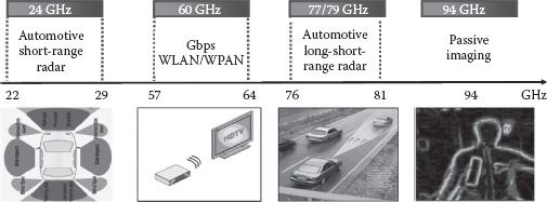
FIGURE 1.1 Miscellaneous MMW applications (frequency boundaries shown in the figure are not accurate).
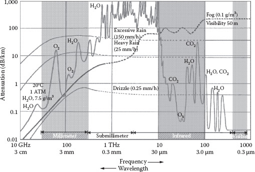
FIGURE 1.2 The attenuation of millimeter waves by atmospheric gases, rain, and fog [4].
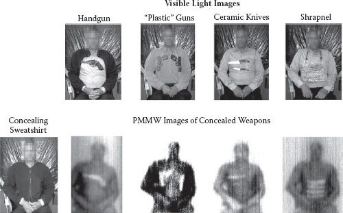
FIGURE 1.3 Passive MMW images [4].
PMMW imaging systems operating near the 94 GHz frequency window provide reasonable balance among capability of currently available silicon technologies, chip size, spatial resolution, and atmospheric attenuation. III-V compound semiconductor technologies have been commonly used as ideal platforms to realize MMW radiometers or passive imaging receivers that are based on multichip modules [6,7]. Recently, benefiting from the aggressive feature size scaling, silicon technology has shown the capability for implementation of W-band passive imaging receivers with fine image and temperature resolution [3,8–9,10]. However, these efforts are limited to a single receiver/pixel. Only recently, efforts have been made to design and implement multipixel imaging array [11–13]. The transition of W-band signals from chip to antenna remains a challenging task, particularly in the context of the multipixel imaging systems. To reduce the scanning time and enable video rate real-time imaging, focal-plane array (FPA) could be used with an array of detectors located at the focal plane of a focusing system [11–13]. Despite non-negligible loss at W-band frequency range, the use of an on-chip antenna can still be advantageous considering the nontrivial electrical interface and assembly cost to implement antenna-in-package or on-board in a multipixel FPA system [12,13]. This chapter provides an overview of the passive imaging design and implementation in silicon technologies.
1.1.2 PASSIVE IMAGING FUNDAMENTALS
This section provides an overview of passive millimeter-wave imaging systems. It covers the basic concept of passive imaging, the miscellaneous applications, the system architecture of a radiometer receiver, the commonly used figure of merit to evaluate passive imaging systems, and the state-of-the-art imaging receivers.
Figure 1.4 shows the block diagram of a total power radiometer, which consists of a low noise RF pre-amplification stage, a square-law power detector, a low frequency amplifier, and an integrator. The radiometer collects the radiated power (PE = kBΔTB) from the target object and produces an output voltage proportional to the incident power. Delta-T is the effective radiometric temperature [4], B is the receiver bandwidth, and kB is the Boltzmann constant.
The sensitivity or the minimum detectable temperature change of an imaging receiver is characterized by a noise equivalent temperature difference (NETD), which is expressed by (1.1) for a total-power radiometer [13,14]:
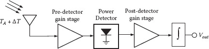
FIGURE 1.4 Block diagram of a total power radiometer.
(1.1) |
where Ts is the system noise temperature, B is the bandwidth, and τ is the integration time, which is typically less than 30 ms (standard video imaging rate) in real-time imaging application.
To build a “useful” imaging system, the NETD needs to be below 1 K, while less than 0.5 K NETD is preferred for good imaging quality [6]. However, the NETD of a total-power radiometer suffers from gain fluctuation, as the RX cannot distinguish between the change in input signal power and the variation of front-end gain. The NETD in the presence of gain fluctuation is given as [14]
(1.2) |
where ΔG/G denotes the total gain fluctuation in percentage. For example, 0.1% gain fluctuation merely translates to an NETD of 3 K for an imaging RX with 3000 K noise temperature. This problem can be solved by periodically chopping above the gain fluctuation frequency using Dicke architecture [15].
Figure 1.5 shows the block diagram of a Dicke radiometer that employs two synchronized single-pole double throw (SPDT) switches: The one at the front end switches between the antenna and a reference load, while the one after the detector demodulates the signal by multiplying it with ±1 in the opposite phase with respect to the front-end switch. In addition to the gain fluctuation problem, the 1/f noise is another source of low frequency disturbance, affecting the system NETD in a similar way. Therefore, the chopping frequency also needs to be higher than the 1/f noise corner frequency.
A power or energy detector serves as the core of an imaging pixel. The common figure of merit to evaluate performance of a power detector is noise-equivalent power (NEP) , defined by (1.3) as a detector’s output rms noise voltage divided by responsivity, R. The responsivity provides a measure of the detector gain and equals the output DC voltage divided by the input RF power—that is,
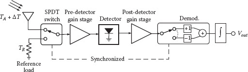
FIGURE 1.5 Block diagram of a Dicke radiometer.
(1.3) |
The NEP and responsivity definitions can be generalized to any power-detecting system—for instance, a power detector preceded by pre-amplification gain stage. In addition to (1.1), there are also other ways to calculate NETD, as reported in May and Rebeiz [3] and Tomkins, Garcia, and Voinigescu [8] and shown in (1.4) and (1.5). The gain fluctuation term is not included in (1.4) and (1.5) for simplicity.
(1.4) |
(1.5) |
NEPdet and NEPsys are the noise-equivalent power of the detector (detector NEP) and imaging RX (system NEP), respectively; G is the total gain preceding the power detector; and kB is the Boltzmann constant. Other parameters carry the same meaning as in (1.1). A brief discussion showing how these formulas are related to each other and how they are applied to different kinds of imaging receivers follows.
For a stand-alone detector acting as a simple imaging RX without any pre-amplification, the NEP rather than NF is the proper measure for noise performance, since the square-law detector is essentially a nonlinear circuit. Therefore, (1.5) should be used to calculate NETD. Note that in this case, NEPsys equals NEPdet. For a direct detection imaging RX consisting of a pre-amplification gain stage (e.g., LNA) and a power detector [3,8,9], both the noise temperature (or NF) of the pre-amplification stage and noise from the detector (measured by NEPdet) contribute to overall system noise. Therefore, the system NETD is obtained either from system NEP, NEPsys, using (1.5) or by superposing the noise contribution from the pre-amplification stage and the detector using (1.4). As clearly seen from (1.4), although the pre-amplification stage also contributes noise denoted by the first term under the square root, it is still required to suppress detector noise in order to achieve a less than 1 K NETD. For a frequency conversion type imaging RX architectures, such as the ones demonstrated in references 10, 12, and 13, where the detector noise is suppressed by high front-end gain, the first term under the square root of (1.4) (representing noise from the front end) dominates and thus (1.4) is simplified to (1.1). In this case, the system NETD calculated from (1.1) and (1.5) should reconcile. Note that a factor of two corresponding to Dicke radiometer needs to be added to all NETD calculations [15].
1.2 SINGLE-PIXELSILICON-BASED PASSIVE IMAGING RECEIVER
Traditionally, radiometers operating at W-band frequency range have been implemented in III-V semiconductor technologies, using multichip systems with module-based level of integration [6]. Figure 1.6 shows a radiometer module that was designed using an imaging chip set consisting of an InP HEMT LNA and an Sb-based backward tunnel diode detector with a horn antenna input and E-plane probe transition. Thermal sensitivity and output noise measurements demonstrate excellent system performance with 0.45 K NETD for a 3.125 ms integration time.
SiGe technologies with fT > 200 GHz have made possible the development of fully integrated, highly compact, passive imaging systems. May and Rebeiz [3] described the design of a W-band passive radiometer chip in a standard 0.12 μm SiGe BiCMOS technology, as shown in Figure 1.7. They presented a total-power radiometer that achieved a temperature resolution of 0.69 K (30 ms integration time) with periodic calibration or chopping above 10 kHz. They also presented a switched Dicke radiometer chip, which addresses the 1/f noise issue of the total-power radiometer and can achieve a temperature resolution of 0.83 K with a 30 ms integration time.
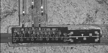
FIGURE 1.6 A W-band radiometer chipset in III-V technology [6].
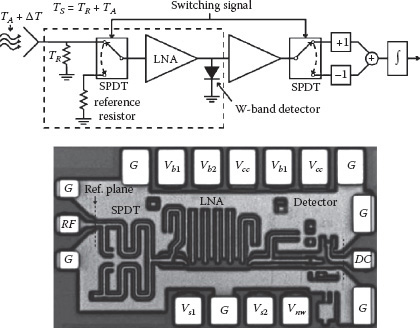
FIGURE 1.7 A W-band single-chip SiGe BiCMOS Dicke radiometer [3].
Although the III-V diodes are not compatible with SiGe/CMOS technology, a high-responsivity, relatively low noise W-band SiGe detector circuit can still be constructed, as shown in Figure 1.8 [3]. The detector is a high-speed SiGe HBT biased in class B regime with a 94 GHz LC notch filter at the output port. The load resistance is chosen to be around 1 k in this design to obtain a high responsivity at video frequencies. The notch filter suppresses the generation of unintended nonlinearities by reducing RF variations in VCE and reduces the effect of transistor collector capacitances.
For the total-power radiometer in May and Rebeiz [3], a five-stage common-emitter LNA was designed and fabricated. The bias currents are chosen for low noise in stages 1 and 2 and for high gain in stages 3–5 (see Figure 1.9). The input transistor is sized to provide simple matching with a near-minimum noise figure. Shunt transmission line stubs and small metal–oxide–metal (MOM) capacitors provide interstage matching. Each stage uses five-layer MOM capacitors beneath the inductive transmission line loads to provide approximately 5 pF of total supply decoupling capacitance at W-band. The 56 Ω transmission line stubs have a signal width, W = 11 μm, and spacing, S = 11 μm, and have Q-factor of 9–1 9–15 from 80 to 100 GHz (including via resistances for connections to transistors) [3]. A deep trench is placed beneath the interstage matching capacitors to reduce substrate coupling. The use of a common-emitter stage, however, raises questions about stability of this LNA. The LNA exhibits higher peak gain of 27 and 24 dB gain across 82–100 GHz [3].
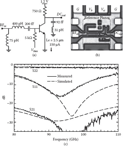
FIGURE 1.8 (a) Detector schematic, (b) chip micrograph (386 × 370 mm2 including pads), and (c) measured S-parameters [3].
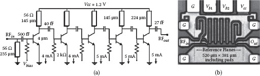
FIGURE 1.9 (a) The five-stage LNA schematic, and (b) the die photo.
1.2.1 A PASSIVE IMAGING RX USING BALANCED LNA WITH EMBEDDED DICKE SWITCH
Typically, the Dicke switch is implemented as an SPDT switch (Figure 1.5) using PIN diodes [16]. This traditional architecture, with a switch right before the LNA, has the drawback of the front-end NF being degraded by the insertion loss of the SPDT switch. This directly results in an increase in NETD. This is not a major problem in III-V technologies, due to the availability of low loss PIN diode switches [17] and, more recently, zero-biased diode detectors [6]. However, silicon-based MMW switches exhibit unacceptably high insertion loss (~5 dB for an HBT switch in a standard SiGe technology). System-level analysis indicates that this 5 dB loss prior to the LNA will degrade the receiver NETD by a factor of approximately three, as shown in Figure 1.10. This degradation, coupled with the inherently high NF of silicon transistors, results in an NETD greater than 0.5 K (which is typically cited as the threshold for acceptable performance in indoor applications [2]). This drawback has been the major motivation behind the front-end architecture shown in Figure 1.11, which promises to eliminate this problem by embedding the Dicke switch functionality within a balanced LNA such that the switch insertion loss contributes minimal effect on the RX’s NF [17]. In this design, the insertion loss of the input coupler directly adds to the front-end NF.
The system comprises a balanced LNA with an embedded Dicke switch, a power detector, and the baseband circuitry [17].
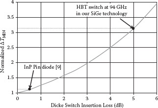
FIGURE 1.10 NETD versus Dicke switch insertion loss.
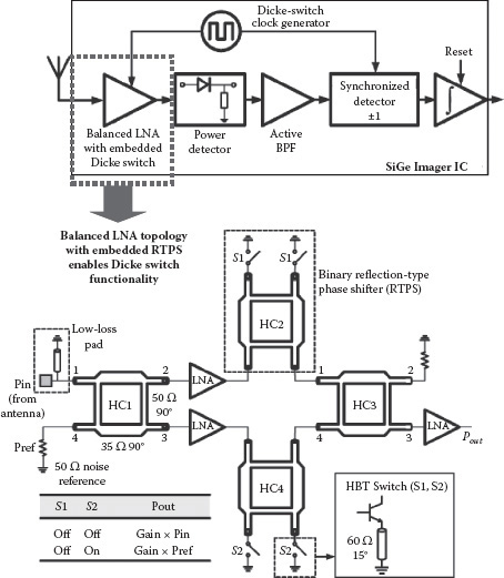
FIGURE 1.11 A W-band direct-detection imaging receiver employing a balanced LNA with embedded Dicke switch.
1.2.1.1 Design and Analysis of Balanced LNA with Embedded Dicke Switch
Figure 1.5 shows the schematic of the balanced LNA (BLNA) incorporating the embedded Dicke switch. Inspired by the GaAs topology first presented in Lo et al. [18], the circuit primarily comprises a balanced LNA with the addition of a reflection-type binary phase shifter in each branch. The operation of this BLNA can be understood using power-waves analysis [19]. Given the well-known S-parameter matrix of a branch-line coupler,
(LC is the insertion loss of the branch coupler), using the superposition principle and assuming input, power waves on ports 1 (antenna port) and 4 (reference port) are expressed as
where aIN,k and θk denote the amplitude and phase of the power wave at the kth port, respectively; we compute the signal magnitude and phase at each point in the BLNA. Note that for this case, the power wave aIN4 represents the noise power of the 50 Ω noise reference. Since the insertion loss LC appears in both gain paths of the BLNA, the power waves of intermediate and output ports are all normalized to LC throughout power-wave analysis.
Port 2 of hybrid coupler HC1 will have the power wave
(1.6) |
and port 3 of HC1 will have the power wave
(1.7) |
For the case when both phase shifters are in the same state, both power waves go through identical paths consisting of LNA gain and phase shift as well as identical attenuation and phase shift due to the reflection-type phase shifters (RTPSs) in Figure 1.11. Therefore, the power wave at port 1 of HC3 will be
where GLNA is the LNA’s gain, LRTPS denotes the RTPS’s loss, and Φ represents the combined phase shift of both the LNA and RTPS. Similarly, the power wave at port 4 of HC3 will be
We then use superposition to compute the power delivered to port 3 of HC3 (i.e., the output port):
(1.8) |
where GTOTAL is the product of the LNA’s gain and the RTPS’s loss. As seen in (1.8), when the phase shifters are in the same state, only a power incident at port 1 of HC1 (aIN1) is present at the BLNA’s output port. However, when the phase shifters are in opposite states, one power wave will experience an additional 180° phase shift. In this case, the power delivered to the output port is expressed as
(1.9) |
This shows that when phase shifters are in opposite states, only power from the 50 Ω reference resistor (aIN4) is delivered to the output port. By toggling between these two states, the desired chopping operation of the Dicke switch is achieved. It can also be shown that when the phase shifters are in opposite states, power from port 1 of HC1 is dissipated in the 50 Ω resistor connected to port 2 of HC3.
To compare NF performance of the BLNA in Figure 1.11 analytically with that of the traditional LNA + switch in Figure 1.7, suppose that each LNA stage in Figure 1.7 exhibits a gain of GLNA. The noise factor of the LNA + switch FSW-LNA in Figure 1.7 is readily expressed as
(1.10) |
where LSW represents the linear loss of the Dicke switch, and FLNA represents the noise factor of the LNA in Figure 1.7. The noise factor of the BLNA with embedded Dicke switch is found to be
(1.11) |
The loss of the hybrid couplers is two to three times (~4 dB) lower than that of SPDT switches. The improvement in noise factor IMF is
(1.12) |
Assuming 20 dB gain for each LNA; 6.5 and 6 dB losses for RTPS and Dicke switches, respectively; and 0.5 dB loss for hybrid coupler, approximately 2.5 dB improvement in NF will be achieved.
Figure 1.12 shows the measured gain and isolation from the antenna and reference ports for the two different phase-shifter states.
As expected, when both phase shifters are in the same state, the signal from the antenna is amplified while the reference signal is suppressed. Conversely, when the phase shifters are in opposite states, the reference input is amplified, while the antenna signal is suppressed. Note that the balanced structure ensures equal gains in both the antenna and reference modes. An additional LNA is used after the balanced structure in order to achieve a total predetection gain of 30 dB, as can be seen in Figure 1.12. The proposed BLNA with embedded Dicke switch achieves a minimum NF of around 9.7 dB.
The BLNA with embedded Dicke switch uses four couplers and three 5-stage LNAs. The LNA in a conventional SPDT structure uses two 5-stage LNAs to achieve almost the same predetection gain and therefore will consume a small chip area. Nevertheless, the BLNA, by virtue of its design, is able to achieve the required NETD for indoor imaging applications. On the other hand, the SPDT architecture (in currently available SiGe technology) essentially cannot. The use of a switch prior to the LNA in the conventional approach degrades the system noise temperature and, therefore, NETD (see Equation 1.4). It is noteworthy that the layout was done conservatively in order to avoid high-frequency EM coupling and to ensure first-pass success. A more aggressive layout approach (e.g., avoiding the use of quarter-wave length bias chokes) can be used to reduce the chip area.
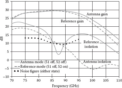
FIGURE 1.12 Measured gain, NF, and isolation for the BLNA.
1.2.1.2 Reflection-Type Phase-Shifter Design
The RTPS structure of Figure 1.13 was chosen because it provides broadband input and output matching. Additionally, the RTPS phase shift stays within ±10% of 180° for the majority of the W-band. Figure 1.13 shows the measured S-parameters as well as measured phase shift for the RTPS structure. The input and output return losses as well as insertion loss of this structure for both possible switch-state operations have been measured. The output return loss was measured to be identical to the input return loss (due to the symmetric nature of the RTPS) and therefore was not included in Figure 1.13. The insertion loss for both operation states is better than –8 dB from 73–100 GHz. It should be noted, however, that this loss comes after 20 dB of LNA amplification and therefore does not contribute to front-end NF as a conventional Dicke switch architecture would.
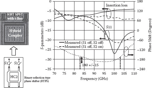
FIGURE 1.13 Measured RTPS S-parameters and phase shift.
1.2.1.3 Five-Stage LNA Design and Analysis
Figure 1.14 shows the maximum available gain (MAG) and minimum achievable NF (NFmin) of a common-emitter HBT in the technology used in this work. The device is optimally sized and biased such that it achieves the lowest NFmin for this technology. Simulations of the single HBT at 90 GHz show a MAG of 3.9 dB and an NFmin of 7.2 dB. A multistage amplifier designed in this technology, therefore, incorporates a first amplifier stage whose gain will not be high enough to reduce the NF contribution of the subsequent stages significantly. Using the well-known Friis equation for the cascaded NF of a multistage amplifier along with the transistor’s MAG and NFmin values, the effect of the latter gain stages on the overall LNA NF can be estimated. It turns out that the second stage will add at least 1.2 dB to the overall LNA’s NF. Adding a third and a fourth stage will contribute 0.4 and 0.1 dB to the overall NF, respectively, resulting in theoretical four-stage MAG and NFmin of 15.6 and 9.0 dB. The previous analysis assumes that each stage achieves maximum gain and minimum NF. However, by design, the first stage of an LNA will trade off a certain amount of available gain in order to achieve the best possible noise match at the input. This, along with loss in the matching networks, necessitates the use of a fifth gain stage in order to achieve the desired 15 dB LNA gain. The fifth stage has a negligible (<0.1 dB) contribution to the LNA NF.
The five-stage common emitter LNA schematic, used inside each LNA block of the BLNA circuit in Figure 1.11, is shown in Figure 1.15. The input matching networks of the first two stages (i.e., the high-pass L- and the π-match networks at the input ports of the first and the second CE stages) are designed to achieve minimum NF.
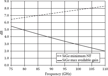
FIGURE 1.14 MAG and NFMIN for the device used in this work across the W-band.
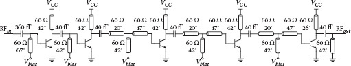
FIGURE 1.15 Five-stage LNA schematic.
These high-pass matching networks reduce the power gain at lower frequencies, where the HBT transistors exhibit naturally high gain, which helps the LNA’s stability. Furthermore, it is desirable to keep the topologies of these matching networks as compact as possible in order to minimize any pregain losses, which will otherwise contribute to higher NF. To achieve the preceding goals, a different design methodology compared to standard silicon-based techniques for obtaining simultaneous power and noise match (presented in Nicolson and Voinigescu [20]) is used. Specifically, due to the low gain of the HBTs in the W-band, inductive emitter degeneration is not employed, thereby avoiding the associated reduction in gain. First, the current density that minimizes the HBT’s NFmin is obtained. In HBT LNAs, as opposed to CMOS LNAs, maximizing fT will not necessarily result in minimizing NFmin because, in HBT devices, an increase in bias current will lead to significantly higher shot noise. The minimum NFmin is thus achieved at a bias current lower than that for maximum fT. The location of the optimum source reflection coefficient, Γopt, for noise match is plotted on the Smith chart, along with the device unmatched input reflection coefficient Γin. The device size is then swept such that Γopt moves sufficiently close to the 50 Ω point on the Smith chart, while at the same time, Γin moves to the same resistance (or conductance) contour as Γopt. This choice of the device size will require only a single stub at the input in order to move the device Γin toward Γopt, thereby achieving excellent noise and impedance match.
Following the methodology described before, an optimum HBT emitter area of 0.75 μm2 is found. Figure 1.16 indicates simulated Γin, Γopt, and the 7.3 dB NF circle (which intersects the 50 Ω point on the Smith chart). As shown in Figure 1.16, Γopt is located on the circle with a constant VSWR of 1.4:1, which corresponds to –15 dB input return loss. A short-circuited stub at the input moves Γin along a constant conductance contour such that it achieves an input noise match within 0.1 dB of NFmin and an input return loss of –15 dB at 90 GHz.
Starting with the output of the second gain stage, all subsequent interstage matching networks employ a more complex T-match network topology realized using transmission lines (t-lines). This matching network offers more degrees of freedom than a single-stub matching network and therefore enables conjugate matching between the output of each stage and the input of the subsequent stage over a larger bandwidth than a single-stub matching network. As a result, maximum power transfer, and hence maximum gain, from the last three stages will be achieved. The insertion loss of the t-lines in the T-match should be minimized, since this loss will reduce the amplifier gain. To this end, t-lines were implemented as slow-wave coplanar waveguide (CPW) structures. A slow-wave CPW (SW-CPW) t-line achieves roughly 60% higher phase shift compared to standard conductor-backed CPW t-lines, for a given length. This translates to reduced loss of the matching networks, as well as reduced chip area.
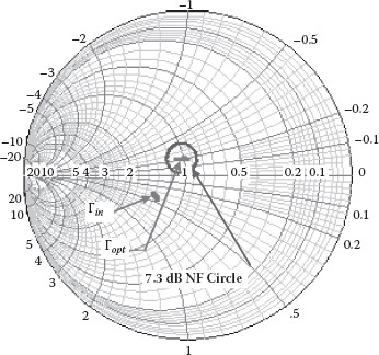
FIGURE 1.16 ΓIN, ΓOPT, and a 7.3 dB NF circle.
The LNA layout has been carefully designed to avoid parasitic feedback across each LNA stage. In particular, every input and output matching stub alternates its orientation in the layout in order to minimize EM coupling between the t-lines and further stabilize the LNA. The simulated k-factor was consistently greater than 10 across the W-band.
On-wafer LNA S-parameters were measured using a VNA with W-band frequency extenders. The VNA measurement results in Figure 1.17 are in good agreement with both theory and simulation, and they show a peak gain of 19 dB at 80 GHz, and better than –12 dB input return loss and –9 dB output return loss from 70 to 110 GHz. NF measurements, shown in Figure 1.17, were performed using a spectrum analyzer (Agilent E4448A) and an external down-converter. The NF was only measured up to 95 GHz due to limitations of the external down-converter. The input and output ports of the LNA were probed with a spectrum analyzer, and no oscillations were observed in the frequency range from 1 to 110 GHz, verifying the stability of the design. The core five-stage LNA draws 35 mA of current from a 1.8 V supply and consumes 1.0 mm2 of chip area.
1.2.1.4 Detector Design and Analysis
The operation principle of a power detector in a direct-detection architecture is to convert the MMW input power to a constant output voltage. Therefore, a linear relationship between input power and output voltage needs to be established. This necessitates that the detector should operate in the square-law region. The detector in this work consists of a pair of common-emitter HBTs, as shown in Figure 1.18. The HBTs are biased via current mirrors and the MMW signal is applied to the base of one of the HBTs. The DC output voltage is taken differentially at the two collectors. Assuming that the input signal is a sinusoidal wave with frequency f and amplitude Vim, the output voltage is expressed as
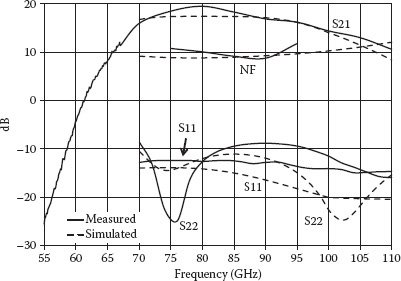
FIGURE 1.17 Measured and simulated five-stage LNA performance.
(1.13) |
where VBE,ON is the bias voltage at the base, VT = kT/q is the thermal voltage, and R is the load resistor. Expanding (1.13) using Taylor series, while truncating higher order terms and leaving the DC output, VOUT becomes approximately equal to
(1.14) |
where IDC is the DC current in each branch, PIN is the input power, RS is the source resistance, and Zin is the input impedance of the HBT.
An important detector figure of merit for imaging applications is the responsivity, which measures the change in detector output voltage per unit input power. From (1.11), the responsivity R can be calculated as
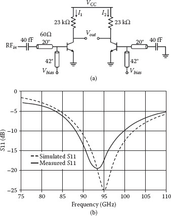
FIGURE 1.18 (a) W-band power detector schematic; (b) simulated and measured detector input return loss.
(1.15) |
where α (in W–1 units) accounts for MMW power transfer due to the input matching network. As can be inferred from (1.15), the responsivity is proportional to the DC current and the load resistor and inversely proportional to the square of the temperature.
The load resistor and HBT device generate three major types of noise at the detector output: shot noise, thermal noise, and flicker noise. Since the Dicke switch is necessarily designed to modulate the PMMW signal above the technology’s 1/f corner frequency, flicker noise can be ignored. The output noise power density is then readily expressed as
(1.16) |
The detector NEP is defined as the minimum input power required for a signal-to-noise ratio of unity at the detector output. From (1.15) and (1.16), the NEP (in W/Hz1/2) is obtained as
(1.17) |
The foregoing analysis provides design insights for a differential HBT-based detector. Most notably, increasing the voltage drop across the load resistor will enhance both the responsivity and the NEP so long as the HBT stays in the forward-active region. Taking this design trend into account, the detector in Figure 1.18(a) is biased to have a collector current of 42 μA and a load resistance of 23 kΩ. As seen in Figure 1.18(a), an input matching network is also used in order to deliver maximum power to the detector input and provide a 50 Ω matched termination at the LNA output.
Figure 1.18(b) shows measured and simulated S11. The detector’s responsivity has been measured using a coherent test setup consisting of a signal generator as a variable input power source and an oscilloscope to measure the output voltage changes. The output spot noise power of the detector was measured using a spectrum analyzer at 1 MHz frequency (the frequency of our Dicke switch).
1.2.1.5 Measurement Results
Figure 1.19 shows the SiGe imaging RX chip micrograph. The power detector is followed by an active bandpass filter with an in-band gain of 20 dB and bandwidth of 0.1–10 MHz, which captures the first nine harmonics of the detector’s output square wave. As mentioned before, all feedback capacitors are implemented using standard on-chip MIM capacitors in the SiGe process, which provides a capacitance density of 2.0 fF/μm2.
In order to evaluate the passive imaging RX performance, relevant imaging parameters have been measured on wafer, with a system integration time of 30 ms. The responsivity of the RX chip is estimated by measuring the integrator’s output voltage with the Dicke switch activated. A baseline calibration is performed before the responsivity measurement in order to estimate the input noise temperature when no signal is applied.
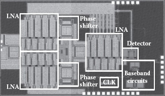
FIGURE 1.19 SiGe imaging RX chip micrograph.
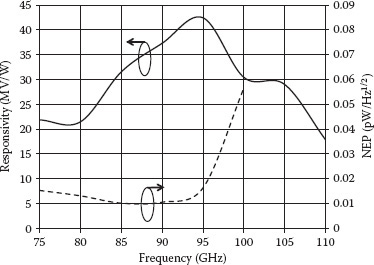
FIGURE 1.20 Measured system responsivity and NEP.
Figure 1.20 shows measured responsivity and NEP versus frequency of the passive imaging RX. The RX achieves a responsivity of 20–43 MV/W across the W-band. The minimum NEP of the imaging system is 10 fW/Hz1/2, which is almost 10 times lower than that of the five-stage LNA + detector. The reason is because the entire integrated imager employs the BLNA of Figure 1.11, whose gain is 11 dB higher than that of the five-stage LNA. Although the base-band op-amp increases the signal level and the output noise, the improvement in NEP is primarily due to higher front-end gain.
Figure 1.21 shows the lab setup for the line-of-sight active measurement of the passive imaging RX. A 12–18 GHz signal generator drives a ×6 multiplier, providing a transmit power of –30 dBm at 90 GHz to a WR-10 horn antenna. The radiated power from the antenna is used to illuminate the object of interest, which, in turn, increases the SNR at the RX input. The RX employs an off-chip narrow-beam horn antenna manufactured by Quinstar Technology. The pyramidal standard gain horn antenna has an aperture size of 26.2 × 20.3 mm2, a midband gain of 24 dB, and a beam width of 11°. The horn antenna is connected through a WR-10 waveguide to the wafer probe. A mechanical drawing of the imaging test setup is shown in Figure 1.22. A simple MMW image of an envelope containing a coin (US quarter) was created and demonstrated in Figure 1.23. The image was generated, one pixel at a time, by stepping the envelope position over a 60 × 40 mm2 area in 5 mm increments. This coarse step was chosen due to the limited accuracy of manual movement of the envelope. The chip output voltage was read on an oscilloscope for each pixel.
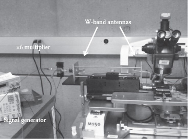
FIGURE 1.21 Imaging test setup.
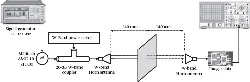
FIGURE 1.22 Imaging test setup diagram.
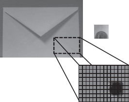
FIGURE 1.23 Image of an envelope containing a coin in visible light and the MMW image.
1.3 FOCAL PLANE ARRAY IMAGING RECEIVERS
The previous section focused on design and implementation of a single receiver/pixel. A real imaging system is, however, required to incorporate multipixel architecture. More precisely, to reduce the scanning time and enable video rate real-time imaging, focal-plane array (FPA) could be used with an array of detectors located at the focal plane of a focusing system [11–13].
In direct detection architecture, discussed in the previous section, the high gain requirement can be met by cascading several LNA stages [3]. Alternatively, one way to improve the sensitivity of a radiometer, without risking oscillation, is to spread gain across multiple frequencies. This can be done using a frequency-conversion type of receiver. Given the fact that the operation frequency is half of fmax for this design, in order to meet the stringent design requirement of the imaging receiver, the direct conversion architecture [10,12,13] is adopted with the LO frequency being placed in the middle of the RF band. Because the input signal is, in fact, broadband noise that contains no phase information, no I/Q path is needed to fulfill down-conversion. The design requirement for the zero-IF amplifier is also relaxed since the IF bandwidth is reduced to one-half of the RF bandwidth. Another advantage of employing direct conversion architecture is that the detector will operate at IF frequency instead of MMW frequency, which leads to lower detector NEP due to higher responsivity and lower output noise. And the lower detector NEP would in turn reduce the required predetection gain for the system to be limited by the front-end noise rather than the detector noise.
The proposed multipixel direct conversion imager architecture is shown in Figure 1.24. The multipixel imager architecture is presented in Figure 1.1. Each RX employs a local frequency tripler whose input is fed by a main 32 GHz PLL [21]. The PLL is shared among the four RXs with the PLL’s output placed at the center of the chip to facilitate skew-minimized LO distribution. An advantage of the proposed scheme is that the LO signal can be generated/distributed at one-third the 96 GHz operation frequency. Each RX (Figure 1.1) consists of a folded slot antenna, an SPDT switch, a four-stage LNA, a single-balanced mixer, an injection-locked frequency tripler (ILFT), an IF VGA, a power detector, a bandpass VGA, and a synchronous demodulator. All signal paths are fully differential after the LNA. An off-chip 200 kHz clock is used to synchronize the SPDT switch with the baseband demodulator for Dicke operation.
1.3.2 RECEIVER BUILDING BLOCKS
1.3.2.1 On-Chip Folded Slot Dipole Antenna
The small antenna form factor at MMW frequency makes it possible for on-chip antenna integration [22–25]. The antenna on-chip solution turns out to be an attractive option for a multipixel FPA imager, since it eliminates the complicated, lossy, and expensive (sub) MMW packaging [11,13]. Despite the benefits of integrating antenna on-chip, the combination of high dielectric constant (εr = 11.9) and low resistivity (8 Ω·cm) of silicon substrate poses a major challenge to on-chip antenna design. The bulk silicon substrate absorbs most of the radiation energy from the antenna into the undesired surface-wave mode due to its high permittivity, and the substrate’s low resistivity leads to electric field loss, which is found to be the dominant loss factor. Several methods [23–25] have been proposed to overcome this problem and improve antenna efficiency. Babakhani et al. [23] attach a hemispherical silicon lens to the bottom of the chip to realize backside radiation. In Wang et al. [24], an off-chip antenna director is placed half a wavelength away from the antenna to guide the electromagnetic wave. In Ahamdi and Naeini [25], a dielectric resonator is built on top of the chip, which enhances the radiation efficiency. However, these solutions either use additional off-chip components [24] or require complex postfabrication processes [23,25]; this makes the packaging even more challenging, reduces the yield, and increases the overall cost.
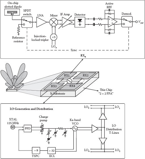
FIGURE 1.24 Block diagram of the 2 × 2 FPA.
Figure 1.25 depicts the three-dimensional view of the SFDA with the CPW feed line used in this design. The folded-slot structure is favored since it provides wide bandwidth, CPW-friendly interface, low metallic loss [22], and high isolation. The advantages of using an SFDA can be better understood by comparing its complementary counterpart—that is, a folded dipole antenna (FDA), shown in Figure 1.26. The FDA is a differential type of antenna that requires balanced excitation from a differential feed line (cf. Figure 1.26). Although this differential type of antenna makes it possible to realize a fully differential RX, the front-end circuits of this chip (SPDT switch and LNA) use single-ended design for the purpose of power/area saving and easy characterization, since there is no four-port W-band VNA available in the lab. Therefore, if the FDA is employed, an additional balun is needed at the antenna interface, which degrades both gain and NF. By interchanging conductive and dielectric material, an FDA is converted to an SFDA, which is excited by a pair of balanced slots instead of balanced metal lines in an FDA. When a signal travels along a single-ended CPW line, a differential electromagnetic field is generated in the two slots between the signal line and the two ground sidewalls. These two slots can thus provide balanced excitation to the SFDA antenna (cf. Figure 1.25). In other words, the CPW feed line provides single-ended interface (through the metal trace) to the front-end circuits and, from the other side, provides differential interface (through the two slots) to the SFDA.
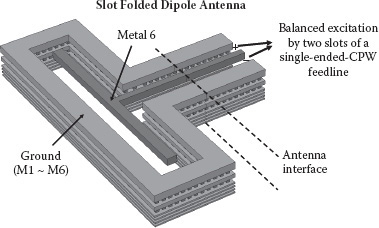
FIGURE 1.25 Three-dimensional view of the slot folded dipole antenna (SFDA).
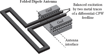
FIGURE 1.26 Three-dimensional view of the folded dipole antenna (FDA).
As shown in Figure 1.25, the ground walls surrounding the slot consist of all metal layers shorted by array of vias in parallel. This configuration leads to several advantages. First, it helps to meet metal density rules for all layers in the vicinity of the antenna. Second, the conductive loss from metals becomes significantly lower compared to FDA, since the current now flows through a much wider path. Third, the ground wall confines the electromagnetic field and prevents mutual coupling between antenna and front-end circuits. In contrast, the radiation pattern of FDA is susceptible to interference from surrounding metal lines or other circuit components. Moreover, the presence of the FDA will also negatively affect the performance of adjacent circuits, especially passive devices like inductors and transformers.
To improve the antenna efficiency further, a patterned deep trench mesh is embedded in the substrate underneath the antenna, as shown in Figure 1.27. In this way, the conductive bulk silicon substrate is decomposed into an array of isolated small squares near its surface. The deep trench available from the technology is 7–10 μm deep from the substrate’s surface and is made of high resistivity material, and the substrate thickness of this process is 280 μm. The deep trench is commonly employed to surround the HBT transistor (as part of the p-cell) to reduce substrate coupling among active devices. The main advantage offered by the deep trench mesh is that it effectively increases the substrate resistance and thus reduces the substrate’s electric field loss, which is the key factor for antenna efficiency. Note that although the depth of the deep trench is much smaller than that of the substrate, it is still effective in improving antenna efficiency because the electric field losses are more pronounced near the substrate’s surface.
To examine the effect of deep trench lattice on antenna performance and validate the preceding analysis, two SFDA test structures have been fabricated and characterized. The two SFDAs have exactly the same design except that one employs deep trench lattice underneath, whereas the other one does not. The measurement results in Figure 1.28 demonstrate an increase in antenna gain by an average value of 2dB as a result of using deep trench lattice. This translates to an efficiency improvement of 1.6 times if antenna directivity is assumed to be the same. The deep trench lattice also reduces coupling between the antenna and other building blocks of the PMMW RX through silicon substrate. In simulation, the SFDA exhibits an efficiency of 16% with deep trench. Figure 1.29 shows the simulated radiation pattern of the SFDA.
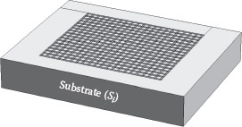
FIGURE 1.27 Silicon substrate with embedded deep trench mesh.
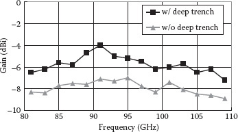
FIGURE 1.28 Measured peak gain of the SFDA with and without deep trench underneath.
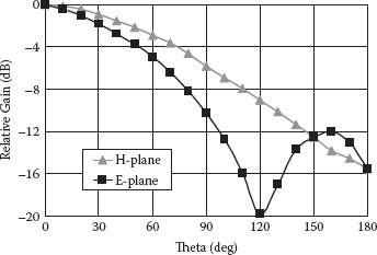
FIGURE 1.29 Simulated radiation pattern of the SFDA.
1.3.2.2 SPDT Switch
The SPDT switch, shown in Figure 1.30(a), is based on a λ / 4 t-line approach similar to the one in Uzunkol and Rebeiz [26]. By turning on and off the shunt NMOS transistor connected to port 1 (or 2), the corresponding branch shifts between isolated and through state. The basic idea is as follows: When the NMOS transistor is turned on (gate voltage equals supply voltage), the drain terminal is shorted to ground. Since a λ / 4 t-line converts “short” to “open,” this branch presents an infinite impedance to port 3 and all the signals will go through the other branch. Because the insertion loss of the switch is directly added to the noise figure, it needs to be minimized for the sake of improving system sensitivity or NETD. In order to reduce insertion loss, we need to minimize the transistor’s on-state resistance and at the same time maximize the off-state (gate voltage = 0 V) impedance.
The on-state resistance of a transistor can be reduced by choosing a large W/L ratio. The off-state impedance can be modeled using a parallel R-C network [26], where the capacitance is tuned out by a shorted t-line stub acting as an inductor and the off-state resistance is highly dependent on the substrate resistance. The substrate resistance can be increased by two layout techniques: (1) surrounding the NMOS device by deep trench, and (2) reducing the number of substrate contacts and placing the contacts several micrometers away from the transistor. Shown in Figure 1.30(b) is the CPW line used in the SPDT switch design with its geometry labeled on the figure. The characteristic impedance is 50 Ω, and the signal line combines M5 and M6 in parallel to reduce loss. The simulated loss at 95 GHz is 0.8 dB/mm. The CPW line uses a ground plane (M1) underneath and two ground side walls to isolate the signal line from the environment.
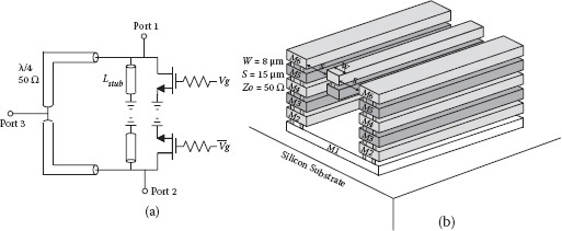
FIGURE 1.30 (a) Schematic of the SPDT switch; (b) geometry of the CPW line used in SPDT switch.
1.3.2.3 LNA
The LNA is a four-stage, single-ended cascode topology (Figure 1.31a). In order to reduce the footprint, lumped inductors (rather than t-lines) are used for output as well as interstage matching. Input matching is designed for minimum NF and is realized using the t-line to avoid layout discontinuity at the interface between the switch and the LNA. The first LNA stage is biased at minimum NF current density, whereas the last three stages are biased for highest gain. Occupying only 380 × 300 μm2 (excluding pad), the LNA breakout circuit exhibits a measured peak gain of 25 dB, 3 dB bandwidth of 20 GHz (86–106 GHz), and a minimum NF of 8.3 dB, as shown in Figure 1.31(b). The LNA draws 21 mA from a 2.5 V supply.
1.3.2.4 LO Generation/Distribution and Tripler
The 32 GHz LO from the PLL is distributed to a local tripler within each RX through a symmetric differential CPW T-line H-tree network with two buffer stages (Figure 1.24). It is found from simulation that to ensure a locking range of >5 GHz for the injection-locked frequency tripler (ILFT), the LO power level at the input of each local tripler should be 1 dBm. The schematic of the ILFT is shown in Figure 1.32. The injection-locking operation is realized by feeding the third harmonic of the input signal generated by Q3 and Q4 into the emitters of a differential Colpitts oscillator. To minimize mutual as well as substrate noise coupling, ground shielded CPW lines (T1 ~ T6) are used at base, collector, and emitter to provide the tank, the load, and part of the degeneration inductances. Additional emitter degeneration inductance is realized by spiral inductor (L1 and L2) to save area. The 96 GHz output signals are taken out from the collector terminals of Q1 and Q2 through a differential cascode buffer. The tripler circuit consumes 70 mW from a 2.5 V supply.
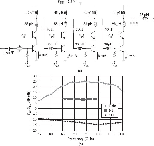
FIGURE 1.31 (a) Schematic and measured performance of LNA; (b) measurement results.
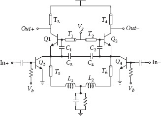
FIGURE 1.32 Schematic of ILFT.
1.3.2.5 Mixer and IF/BB Circuitry
A single-balanced mixer is adopted for better noise performance. Further LO rejection is provided by the IF VGA, which is based on Cherry-Hopper topology with 10–20 dB of variable gain. Finally, power detection is realized using a common-emitter-based square law detector.
The front-end RX achieves 34–44 dB variable gain and 11.3 dB minimum NF, as shown in Figure 1.33. The PLL and tripler together exhibit a measured tuning range of 92.67–98.2 GHz, which is limited by the locking range of the ILFT. Using a 125 MHz crystal oscillator (CVHD-950) as reference, the PLL + tripler’s phase noise at 96 GHz is –93 dBc/Hz at 1 MHz offset (Figure 1.34).
A chip-on-board solution was used to evaluate the system performance. Figure 1.35 shows the measured responsivity (antenna de-embedded) and the NEP referred to the input of the switch for RX1. The average responsivity and NEP over 3 dB BW are 285 MV/W and 8.1 fW/√Hz, respectively. Imaging functionality of the 2 × 2 FPA was verified using an incoherent source in a transmission mode measurement setup [11,13], shown in Figure 1.36. Image of a metallic object inside an envelope is constructed by mechanically scanning the chip and mapping the output voltage of each pixel to corresponding grayscale intensity.
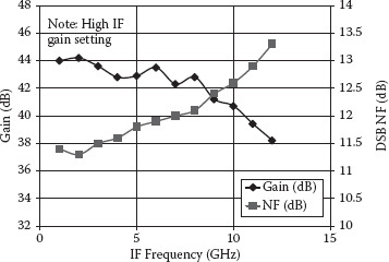
FIGURE 1.33 Measured receiver front-end gain and NF.
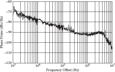
FIGURE 1.34 Measured 96 GHz phase noise.
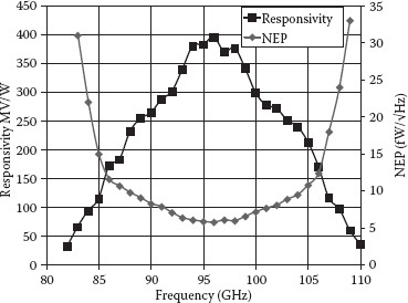
FIGURE 1.35 Measured single RX responsivity and NEP.
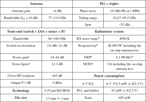
The complete measured performance of the 2 × 2 FPA is summarized in Table 1.1. The imaging chip achieves a calculated NETD of 0.48 K with 30 ms integration time. The chip is fabricated in a 0.18 μm SiGe BiCMOS process and occupies an area of 3.5 × 3 mm2 (Figure 1.37).
The author thanks all PhD members of the NCIC Labs, including Zhiming Chen, Chun-Cheng Wang, Vipul Jain, and Leland Gilreath. The author also thanks TowerJazz Semiconductor for chip fabrication. This work has been supported in part by an NSF grant under contract ECCS-1002294 and an SRC grant under contract 2009-VJ-1962.
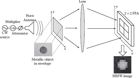
FIGURE 1.36 Imaging system measurement setup and MMW image.
a Includes switch loss.
b Average over 3 dB bandwidth.
c A factor of 2 was included for Dicke switching; assumes 30 ms integration time; calculated with measured NEP.
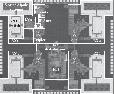
FIGURE 1.37 Die micrograph of the 2 × 2 FPA.
1. C. Marcu, D. Chowdhury, C. Thakkar, J.-D. Park, L.-K. Kong, M. Tabesh, Y. Wang, et al., A 90 nm CMOS low-power 60 GHz transceiver with integrated baseband circuitry. IEEE Journal of Solid-State Circuits, vol. 44, no. 12, pp. 3434–3447, Dec. 2009.
2. V. Jain, F. Tzeng, L. Zhou, P. Heydari, A single-chip dual-band 22–29 GHz/77–81 GHz BiCMOS transceiver for automotive radars. IEEE Journal of Solid-State Circuits, vol. 44, no. 12, pp. 3469–3485, Dec. 2009.
3. J. W. May, G. M. Rebeiz, Design and characterization of W-Band SiGe RFICs for passive millimeter-wave imaging. IEEE Transactions Microwave Theory & Technology, vol. 58, no. 5, pp. 1420–1430, May 2010.
4. L. Yujiri, M. Shoucri, P. Moffa, Passive millimeter wave imaging. IEEE Microwave Magazine, vol. 4, no. 3, pp. 39–50, Sept. 2003.
5. R. Appleby, R. N. Anderton, Millimeter-wave and submillimeter-wave imaging for security and surveillance. IEEE Proceedings, vol. 95, no. 8, pp. 1683–1690, Aug. 2007.
6. J. J. Lynch, H. P. Moyer, J. H. Schaffner, Y. Royter, M. Sokolich, B. Hughes, Y. J. Yoon, J. N. Schulman, Passive millimeter-wave imaging module with preamplified zero-bias detection. IEEE Transactions Microwave Theory & Technology, vol. 56, no. 7, pp. 1592–1600, July 2008.
7. W. R. Deal, L. Yujiri, M. Siddiqui, R. Lai, Advanced MMIC for passive millimeter and submillimeter wave imaging. IEEE ISSCC Digest Technical Papers, pp. 572–573, Feb. 2007.
8. A. Tomkins, P. Garcia, S. P. Voinigescu, A passive W-band imaging receiver in 65 nm bulk CMOS. IEEE Journal of Solid-State Circuits, vol. 45, no. 10, pp. 1981–1991, Oct. 2010.
9. L. Gilreath, V. Jain, P. Heydari, Design and analysis of a W-band SiGe direct-detection-based passive imaging receiver. IEEE Journal of Solid-States Circuits, vol. 46, no. 10, Oct. 2011.
10. L. Zhou, C.-C. Wang, Z. Chen, P. Heydari, A W-band CMOS receiver chipset for millimeter-wave radiometer systems. IEEE Journal of Solid-States Circuits, vol. 46, no. 2, pp. 378–391, Feb. 2011.
11. E. Ojefors, U. R. Pfeiffer, A. Lisauskas, H. G. Roskos, A 0.65 THz focal-plane array in a quarter-micron CMOS process technology. IEEE Journal of Solid-State Circuits, vol. 44, no. 7, pp. 1968–1976, July 2009.
12. C.-C. Wang, Z. Chen, H.-C. Yao, P. Heydari, A fully integrated 96 GHz 2 × 2 focal-plane array with on-chip antenna. IEEE RFIC Symposium Digest, pp. 357–360, June 2011.
13. Z. Chen, C.-C. Wang, P. Heydari, A BiCMOS W-band 2 × 2 focal-plane array with on-chip antenna. IEEE Journal of Solid-State Circuits, vol. 47, 2012.
14. M. Tiuri, Radio astronomy receivers. IEEE Transactions on Antennas and Propagation, vol. 12, no. 7, Dec. 1964.
15. R. H. Dicke, The measurement of thermal radiation at microwave frequencies. Reviews Scientific Instruments, vol. 17, pp. 268–275, July 1946.
16. C. Martin et al., Rapid passive MMW security screening portal. Proceedings of SPIE Defense and Security 2008, vol. 6948.
17. V. Ziegler et al., Low-power consumption InGaAs PIN diode switches for V-band applications. Japan Journal of Applied Physics, vol. 38, pp. 1208–1210, 1999.
18. D. C. W. Lo et al., Novel monolithic millimeter wave multi-functional balanced switching low noise amplifiers. IEEE Transactions Microwave Theory and Techniques, vol. 42, no. 12, pp. 2629–2634, Dec. 1994.
19. G. Gonzalez, Microwave transistor amplifiers: Analysis and design, 2nd ed. Englewood Cliffs, NJ: Prentice Hall, Aug. 1996.
20. S. T. Nicolson, S. P. Voinigescu, Methodology for simultaneous noise and impedance matching in W-band LNAs. Proceedings IEEE Compound Semiconductor Integrated Circuits Symposium, pp. 279–282, Nov. 2006.
21. Z. Chen, C.-C. Wang, P. Heydari, W-band frequency synthesis using a Ka-band PLL and two different frequency triplers. IEEE RFIC Symposium Digest, pp. 83–86, June 2011.
22. A. Arbabian, S. Callender, S. Kang, B. Afshar, J.-C. Chien, A. M. Niknejad, A 90 GHz hybrid switching pulsed-transmitter for medical imaging. IEEE Journal of Solid-State Circuits, vol. 45, no. 12, pp. 2667–2681, Dec. 2010.
23. A. Babakhani, X. Guan, A. Komijani, A. Natarajan, A. Hajimiri, A 77 GHz phased-array transceiver with on-chip antennas in silicon: Receiver and antennas. IEEE Journal of Solid-State Circuits, vol. 41, no. 12, pp. 2795–2806, Dec. 2006.
24. C.-H. Wang, Y.-H. Cho, C.-S. Lin, H. Wang, C.-H. Chen, D.-C. Niu, J. Yeh, et al., A 60 GHz transmitter with integrated antenna in 0.18 μm SiGe BiCMOS technology. IEEE ISSCC Digest Technical Papers, pp. 659–660, Feb. 2006.
25. M. R. N. Ahamdi, S. S. Naeini, On-chip antennas for 24, 60, and 77 GHz single package transceivers on low resistivity silicon substrate. IEEE Symposium Antennas and Propagation, pp. 5059–5062, 2007.
26. M. Uzunkol, G. M. Rebeiz, A low-loss 50–70 GHz SPDT switch in 90 nm CMOS. IEEE Journal of Solid-State Circuits, vol. 45, no. 10, pp. 2003–2007, Oct. 2010.