
Large Signal and Small Signal Building Blocks for Cellular Infrastructure |
|
CONTENTS
7.2 Fully Integrated, High Performance, Low Noise Amplifier
7.3 Flexible, High Efficiency Radio Frequency Power Amplifier Designs
7.3.1 Switched Mode Wideband Class-E Out-Phasing Power Amplifier
7.4 Highly Integrated RF Power Amplifiers in CMOS Technology
7.4.1 RF Power Amplifier with Wideband Transformer Combiner
7.4.2 Broadband Class-E RF Power Amplifier
Mobile wireless communications have become a mainstream technology for everybody; the number of subscribers is expected to hit five billion subscriptions in 2011. Network operators have experienced a strong increase in demand for fast mobile broadband applications, which are also the focus of more recent releases for cellular communications standards as frequency spectrum for cellular applications is limited. The desired high data rates come at a price: Ever more complex modulation schemes and fairly high signal-to-noise ratios in increasingly smaller cells are required to support high speed operation. Spatial diversity multiple input multiple output (MIMO) schemes using several antennas per radio channel will become the norm in cellular infrastructures (i.e., base station designs, which aim at offering the maximum throughput to the mobile user). Network operators are faced with an increasing need for flexible solutions; installation costs and operating expenses need to come down as well in order to be able to deal with the increase in number of cell sites needed to offer adequate coverage and capacity in a given area. This requirement calls for highly integrated solutions to address cost; radio frequency (RF) power amplifiers with a high DC power efficiency along with new base station partitioning options such as remote radio head units significantly reduce the operating expenses.
There are actually only a few key building blocks in the analog domain for cellular infrastructure. Low noise amplifiers, frequency conversion mixers, and radio signal drivers and power amplifiers are the main ones. Implementing these in silicon-based process technologies allows one to meet the cost and performance targets while offering a high level of integration at the same time. In the following sections a number of examples will be given that demonstrate the capabilities of recent integrated circuit designs in the field of analog components for cellular infrastructure and the methodologies applied to reach this achievement.
7.2 FULLY INTEGRATED, HIGH PERFORMANCE, LOW NOISE AMPLIFIER
Low noise amplifiers (LNAs) for wideband code division multiple access (W-CDMA) base stations need to meet two key requirements. Firstly, a noise figure below 1 dB at operating frequencies in the cellular bands from 700 up to 2700 MHz is required for optimal receiver sensitivity. Secondly, the interference resulting from operations in adjacent frequency channels demands high linearity and thus low third-order intermodulation distortion.
Two alternative semiconductors materials technologies have been applied in the past to meet these requirements. The classical solution is amplifiers based on GaAs pHEMT devices (e.g., references 1 and 2). They do not have problems achieving the low noise and high linearity requirements but suffer from the lack of protection against electrostatic discharge (ESD), low level of integration, and the need for costly external, high quality passive components to implement impedance matching while maintaining optimum noise performance. Historically, LNA designs based on pure Si process technology, the second alternative, were not very efficient or had difficulties meeting all requirements. Some designs have been reported in the past, but they either had difficulties achieving the target specifications or did not implement 50 Ω impedance matching [3–4,5].
We introduce a fully integrated LNA design based on advanced Si technology that is able to overcome the issues associated with III-V compound technologies mentioned earlier. A 0.25 μm SiGe:C BiCMOS technology has been used to implement a two-stage LNA design [6]. The process technology offers active devices with a cutoff frequency ft of 130 GHz. The first stage, an NPN device with an emitter width of 0.4 μm, is optimized for a noise figure of 0.5 dB at 2 GHz operating frequency and a gain of more than 10 dB at the same frequency. It is operated at 1.8 V supply voltage. The second stage is operated at 3.0 V supply voltage and is designed to meet the linearity requirements. It provides 15 dB gain at a noise figure of 0.7 dB.
The starting point for the development of the input stage was a single transistor design with 17 dB DC gain, an emitter length of 10 μm, and a DC bias current of 1.3 mA. Simulation results have shown that this design would not allow simultaneous input impedance match and noise match, and the OIP3 would be about–12 dBm for a gain Gmax of close to 15 dB. In order to improve the linearity of the input stage and at the same time bring the input and optimum noise impedances back to acceptable values, 12 identical transistor stages have been connected in parallel at the expense of a 16 mA bias current. This arrangement lowers the impedances by the same factor of 12 and raises the OIP3 to +27 dBm while maintaining a noise figure close to the minimum noise figure of 0.5 dB.
Following a similar strategy for the second stage, which is optimized to match the high linearity requirement, its design employs 30 identical stages in parallel, each using a high voltage device with an emitter width of 20 μm. The second stage draws 54 mA DC current from a 3 V supply voltage and achieves an OIP3 of +40 dBm and a noise figure of around 0.7 dB. The circuit diagram of the complete low noise amplifier is shown in Figure 7.1 along with a microphotograph of the chip.
For the final design, which combines the two stages, special attention had to be paid to the impedance matching at input, interstage, and output levels. A tapped load inductor at the output of the first stage is chosen to lower the output impedance of the first stage to 5–10 Ω, which is closer to the 3 Ω input impedance of the second stage. The matching is further improved by adding a degeneration inductor in the emitter path of the first stage combined with a shunt capacitor at its collector output and a feedback capacitor from the collector output of the second stage back to its base to achieve a flatter frequency response. ESD protection circuitry has been added to all relevant pins, a feature not available in III-V compound technologies.
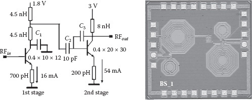
FIGURE 7.1 The low noise amplifier comprises a low noise input stage and an output stage optimized for high linearity. It is manufactured in SiGe:C BiCMOS technology, and the chip area is 1.1 × 1.3 mm2. The chip microphotograph is shown on the right.
The final design features a die size of 1.1 × 1.3 mm2 and consumes a total power of 190 mW: 16 mA at 1.8 V supply voltage and 54 mA at 3 V supply. The devices were packaged in an HVSON10 package and mounted on a printed circuit board for testing. The measured noise performance indicates that an almost optimal noise match at the input has been obtained. The noise figure is 0.75 dB in the 900 MHz GSM band and 0.9 dB in the 1800 MHz band; it remains below 1 dB up to 2 GHz operating frequency (see Figure 7.2, left). At 900 MHz operating frequency a gain ∣S21∣ of 34 dB has been realized; at 1.8 GHz the measured gain was 24 dB. An important parameter in cellular systems design apart from the absolute gain value is its flatness within an 80 MHz wide frequency band. At frequencies of 900 MHz the gain flatness is better than 1 dB. For frequencies higher than 1.8 GHz the flatness improves to even better than 0.6 dB.
A very good input impedance match to 50 Ω has been achieved over a wide range of input frequencies; the input return loss S11 is better than 18 dB at the W-CDMA operating frequencies. The input return loss is better than 10 dB in the frequency range between 750 MHz and 2.4 GHz.
Two-tone linearity tests according to test standards (i.e., with tones 1.5 MHz apart) have been carried out on the devices in the 900 MHz frequency band. The devices exhibit an output IP3 of +36 dBm and a 1 dB output compression point of +19 dBm (see Figure 7.2, right). Linearity tests with two tones at 1800 MHz produced similar results. Compared to the more conventional, largely discrete solutions based on compound semiconductor technologies, the present fully integrated LNA design offers the additional benefits of including ESD protection on all its pins including the RF input/output pins and offering an input impedance matched to 50 Ω without the need for external matching components.
This Si-based two stage LNA design is an example that noise figures below 1 dB combined with high linearity performance are possible. Even though III-V compound technologies may offer better noise figures, the present design can offer more robustness through integrated ESD protection and a higher level of integration while meeting target specifications.
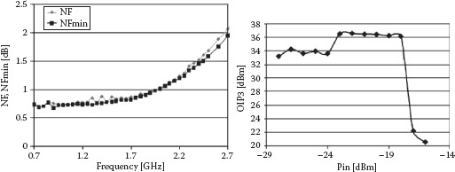
FIGURE 7.2 The low noise amplifier design meets the target specifications for application in cellular infrastructure. The noise figure stays below 1 dB up to 2 GHz. The LNA achieves an OIP3 of 36 dBm.
7.3 FLEXIBLE, HIGH EFFICIENCY RADIO FREQUENCY POWER AMPLIFIER DESIGNS
In modern cellular communication systems the RF power amplifier has to deal with modulated signals, which employ a high peak-to-average ratio. Complex digital modulation schemes are used to achieve communication at high data rates while using the available bandwidth efficiently. In these modulation schemes both the phase and the amplitude of the carrier signal are being modulated. As a result high requirements are imposed on the linearity of the transmitter and particularly its power amplifier. A base station transmitter design needs to address the challenge to preserve high linearity and high power efficiency over a wide operating frequency range in order to decrease overall power consumption and heat dissipation, ultimately leading to lower operating cost for the network operator.
7.3.1 SWITCHED MODE WIDEBAND CLASS-E OUT-PHASING POWER AMPLIFIER
An out-phasing power amplifier is an old concept [7] applied to the challenges of current communications systems in an attempt to address the linearity–efficiency trade-off; it is based on linear amplification using nonlinear components. A switched mode power amplifier takes this concept to the extreme in that it does not even attempt to preserve any amplitude information, but rather applies hard switching of the output stages in order to achieve very high power added efficiency (PAE). In an out-phasing transmitter, the complex modulated input signal is decomposed into two signals with constant amplitude and a relative phase difference θ corresponding to the time-varying envelope of the original input signal. The two branch signals are amplified separately in highly efficient switch-mode output power stages. The two amplified signals are finally added to produce the desired complex signal with time-varying amplitude using trigonometric equalities. In the 19 W RF output power class-E power amplifier described here, the addition is implemented in a modified Chireix combiner, which offers a particularly wide operating bandwidth [8]. The output stage of the amplifier employs GaN power transistors for the nonlinear switching type amplification and a dedicated CMOS (complementary metal oxide semiconductor) driver circuit.
7.3.1.1 Details of the Design
The challenge in the design of the CMOS driver circuit is associated with the high input capacitance of the GaN power switch transistors. The gates of the GaN transistors need to be driven with pulsed signals at radio frequency with amplitudes exceeding 5 Vpp in order to achieve the fast switching times required for very high PAE and drain efficiency. These voltage swings are not in line with the voltage handling capabilities of regular CMOS technologies and as a result high voltage handling capabilities have to be added to the design. Instead of the device-stacking technique most commonly used to achieve high voltage performance extended drain, thin oxide MOS (EDMOS) transistors have been employed in this driver design [9]. The EDMOS transistors have been added to a 65 nm low voltage CMOS process technology without extra masks or process steps. They achieve a breakdown voltage of 12 V while offering transit frequencies fT beyond 30 GHz. The resulting high speed driver can deliver 8 Vpp output swing up to 3.6 GHz [17].
The final output stage of the driver circuit consists of an EDMOS-based inverter stage. The EDMOS inverter stage can be driven directly by low voltage, high speed standard CMOS inverters, allowing for easy interfacing to the digital logic, which generates the modulated input signals, and integration on the same die. Three CMOS inverter stages in series with increasingly larger transistor geometries have been used. Throughout the design of the driver circuit a unitary P (positive) MOS to negative (N) MOS transistor size ratio has been maintained with the intention to achieve optimum layout symmetry between the two RF paths prior to the output stage. Each transistor of the four stages employed is actually made up of a large number of unit transistor parameterized cells (P-cells); they all feature minimum gate length and have gate widths of 240, 480, 1440, and 4032 μm (EDMOS device), respectively. Figure 7.3 outlines the overall block diagram of the driver circuit.
The driver design includes large on-chip AC-coupling and -decoupling capacitors. They are implemented as parallel-plate interdigitated metal-fringe capacitors. The input coupling capacitors have a capacity of 16 pF each and also implement the level shifter in combination with two DC input biasing lines. For the output pins, DC-coupled and AC-coupled outputs are available, the latter using a 49 pF coupling capacitor. Besides using thick and wide power supply lines, on-chip decoupling capacitors are also integrated on chip using four capacitors for a total decoupling capacitance of about 700 pF. The total chip area of the driver device is 1.99 mm2; the EDMOS output stage and the inverter driver stages consume just 0.16 mm2.
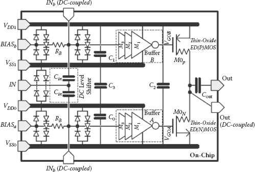
FIGURE 7.3 Circuit diagram of the CMOS driver device. Three conventional CMOS inverters amplify the input signals and drive the EDMOS output stage transistors. Level shifting and decoupling capacitors are integrated on chip.
The CMOS driver has pulse-width control capabilities built in over the output square wave signal. A variable gate bias technique has been applied to achieve the required pulse-width modulation. This approach offers a way to perform fine adjustment and tuning functionality to enhance the performance of a switched mode RF power amplifier. The bias level of the first inverter of the two parallel paths shifts up/down the sinusoidal RF input signal with respect to the inverter’s own switching threshold. A change on this bias voltage will vary the pulse width at the output of this inverter; the resulting pulse-modulated signals are then propagated through following two inverter stages before they are combined at the output of the two EDMOS output transistors.
For the final RF output amplifier the driver circuit is combined with two RF output power transistors (see Figure 7.6). The RF power output stage switches are realized in 28 V GaN HEMT technology; they are driven by one such CMOS driver circuit each. The CMOS drivers are capacitively coupled to the gates in order to support the negative bias voltage needed for the GaN switches. The desired amplified output signal is available after combining of the two branch signals. Ideally, a transformer would be used to merge the two signals into a combined output signal. However, a lumped element transformer is difficult to implement for high output power levels at radio frequencies. A Chireix combiner [7] attempts to implement the summation function by using transmission lines connecting the two switch outputs to the common output load; in its classical form it employs quarter wavelength transmission lines with extra compensation elements either as lumped elements or integrated in the combiner itself. Despite its elegant design, some drawbacks in the context of switched mode out-phasing power amplifiers needed to be addressed. With the conventional Chireix combiner, the efficiency would depend not only on the out-phasing angle but also on the operating frequency because both the Chireix compensation elements and the properties of the quarter wavelength transmission lines are frequency dependent [10]. This would be highly undesirable for a class-E out-phasing amplifier, especially under the intended wide bandwidth operation.
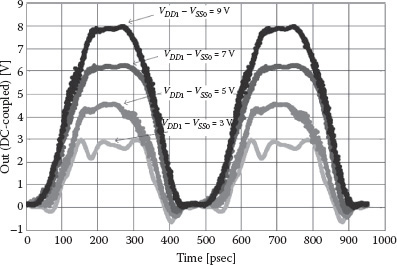
FIGURE 7.4 The CMOS driver circuit can deliver signal output swings up to 8.04 Vpp when operating from a 9 V supply voltage and driving a 50 Ω load. This performance can be maintained for operating frequencies reaching 3.6 GHz.
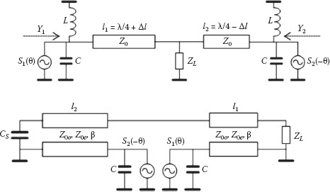
FIGURE 7.5 Schematic block diagrams of the original Chireix combiner (left) and the combiner based on coupled transmission lines (right).
In order to increase the operational bandwidth of the combiner, the quarter wavelength transmission lines of the conventional Chireix combiner design were replaced by coupled transmission lines meant to implement a transformer like behavior (refer to Figure 7.5). This combiner approach makes it possible to achieve improved efficiency over a wide peak-to-average ratio power range and increased RF bandwidth by removing some of the frequency dependent behavior of the original Chireix combiner.
For a more detailed analysis we start with the conventional Chireix combiner and derive some of the critical design parameters from its equivalent circuit diagram [8]. The prototype admittance conditions needed at the drain terminal of the transistor switches in order to establish the desired class-E terminations and also the Chireix compensation elements can be found to be
In this equation, BE,LM and GE,LM are the optimum class-E susceptance and conductance for load modulation, respectively. For an optimum design parameter q = 1.3, they can be approximated as
For this choice of design parameter q we observe that if the load resistance changes from its nominal to a higher value, the class-E power amplifier responds to this change by changing its turn-on voltage slope to a negative slope while keeping its turn-on voltage close to zero. By doing so, the efficiency is preserved for the varying load conditions that can occur on an out-phasing amplifier. The required Chireix compensation susceptance is then defined by the following formula:
With these intermediate results, the element values for the actual Chireix combiner using coupled transmission lines can be determined by equating the prototype admittance of the original combiner to the input port admittances of the new coupled transmission line combiner. A necessary condition is that at one side of the coupled transmission line combiner is terminated with a capacitor C as given by
This capacitor will tune out the leakage inductance of the coupled transmission line “transformer” element. The electrical lengths βl1 and βl2 of the coupled transmission line combiner are unequal due to the Chireix compensation elements and can be calculated to be
The last design step for the new Chireix combiner approach is to determine the optimum even-mode and odd-mode impedances Z0e and Z0o. The odd-mode impedance Z0o can be calculated based on the impedance transformation from the output (ZL) to the input port impedances Z1 and Z2:
In this equation, n = Z0e/Z0o and should be large so as to maximize the magnetic coupling in the coupled transmission line “transformer” element. With these modifications we achieved an improvement in operating bandwidth by a factor of two for a coupling factor k = 0.88.
7.3.1.2 Measurement Results
The CMOS driver circuit was first tested in a stand-alone test setup with the die directly mounted on a printed circuit board. The tests were carried out in a 50 Ω load environment. The input of the device was driven with a sinusoidal input signal at 2.1 GHz. The output signal at the DC-coupled output pin was monitored using a high speed digital sampling oscilloscope for supply voltages between 3 and 9 V. The maximum output voltage swing observed was 8.04 Vpp for a 50 Ω load and a 9 V supply voltage. The output signal traces for a variety of supply voltages are shown in Figure 7.4. An on-resistance of the driver output of 4.6 Ω was measured. The ability to apply pulse width modulation to the input signal was also tested. At 2.4 GHz operating frequency and with 5 V supply voltage, a control range of the duty cycle between 30.7% and 71.5% was measured. The driver circuit achieves a much higher output voltage swing and higher operating frequency than previously reported state-of-the-art designs in CMOS [11]. Its performance is comparable to that achieved with designs in SiGe BiCMOS technology [12] with the extra benefit of pulse width control capability and better efficiency.
A demonstrator out-phasing switched mode RF power amplifier has been built using the aforementioned CMOS driver circuit in combination with GaN devices and the modified coupled transmission line Chireix combiner discussed before. A fourth-order Butterworth matching filter connected to the output of the combiner transforms the 50 Ω antenna impedance to the required class-E load and also sets the required loaded quality factor. In this demonstrator the Chireix combiner is built with symmetrical broadside coupled transmission lines, which are implemented between the top metal layers in a dual-layer Rogers laminate with a dielectric constant εr = 3.5. The top layer is 0.1 mm thick and nearly level with the surface of the GaN switch device dies that are attached directly to the flange. The bottom layer is 1 mm thick and terminated with a metal ground plane. The layer thickness aspect ratio basically determines the maximum ratio between the even-mode and odd-mode impedance of the coupled transmission line implementation.
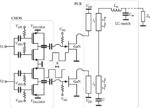
FIGURE 7.6 The out-phasing class-E RF power amplifier consists of the three stages CMOS input driver, GaN output switch transistors, and Chireix combiner using coupled transmission lines. It can achieve a high DC power efficiency over a broad operating frequency range.
The CMOS driver devices are mounted close to the two GaN output transistor switches in order to allow for short bond wires when connecting the two devices via chip-to-chip bonding. This will minimize the inductance of the bond wires and helps to maximize the signal bandwidth of the interface. A similar approach is used for the wiring to the laminate input and output connections. Figure 7.7 shows the CMOS driver chips, the two GaN power switch transistors, and the bond wire connections in more detail.
The demonstrator class-E out-phasing switched mode power amplifier module has been characterized using a dedicated measurement setup capable of acquiring single-tone data and analyzing the performance of the power amplifier with complex modulated input signals including predistortion. The module has been evaluated by sweeping a single tone from 1.75 to 2.1 GHz. The drain efficiency is defined as the RF output power at the 50 Ω connector interface divided by the DC power supplied to the drains of the GaN switch transistors. The total lineup efficiency also includes the power dissipated by the CMOS driver and the RF input power delivered to the inputs of the module. The peak power and drain efficiency have been measured over the given frequency range for a number of back-off scenarios. The peak power is about 42.4 dBm and varies only 0.7 dB over the frequency range (see Figure 7.8). The drain efficiency varies with the power back-off as a result of the change in load impedance of the combiner with the phase difference applied and is better than 60% over a bandwidth larger than 250 MHz for 6 dB back-off, 150 MHz for 8 dB back-off, and 70 MHz for 10 dB back-off. At 10 dB back-off the drain efficiency is 65% and the total lineup efficiency is 44%. For an 8 dB back-off the results change to a drain efficiency of 70% and a total lineup efficiency of 53%. Even though the present switched mode RF power module is a two-way system, the drain efficiency at 10 dB back-off is comparable to what has been reported previously for a three-way GaN Doherty power amplifier [13]—but now with the extra benefit of better broadband capabilities and the integration of a CMOS driver stage, which enables direct digital steering of the power amplifier.
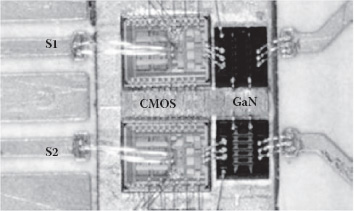
FIGURE 7.7 Chip microphotograph showing details of the assembly of the CMOS driver circuit and the GaN output switching transistors on the Rogers laminate substrate. Multiple bond wire connections are used for most of the signals so as to lower the inductance and thus improve the signal bandwidth.
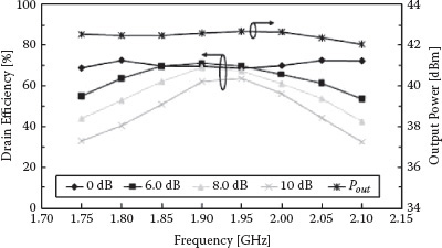
FIGURE 7.8 The out-phasing class-E RF power amplifier achieves an output power level of about 42 dBm over a wide operating frequency range. The DC power efficiency is better than 60% over a 250 MHz frequency range at 6 dB power back-off; at 10 dB back-off it can maintain this efficiency level over a range of more than 70 MHz.
7.4 HIGHLY INTEGRATED RF POWER AMPLIFIERS IN CMOS TECHNOLOGY
For base station designs targeting very small cells such as pico and femto cells, a more fully integrated solution may be preferred by the network operators. The possibility of full integration of the RF power amplifier with the CMOS transceiver and baseband subsystems is of particular interest. The expected RF output power is usually below 30 dBm. Even at these relatively low RF output power levels, the designer needs to choose between a more linear power amplifier design with its associated poor power efficiency and a highly nonlinear switched-mode design, which is much more power efficient.
In the following sections two examples will be given for RF power amplifier designs that are implemented in bulk 65 nm CMOS technology. Besides their application in small cell base stations, they can also serve as amplifiers in mobile terminals. The implementation of CMOS RF power amplifiers in a standard CMOS technology is a challenging task due to the associated low breakdown voltage of the active devices. Lately, devices with high breakdown voltage, such as extended drain MOS (EDMOS) and thick-oxide MOS transistors, have gained increased interest [9]. Such devices can withstand a higher drain-source voltage than regular CMOS transistors and are therefore able to deliver more RF output power reliably.
7.4.1 RF POWER AMPLIFIER WITH WIDEBAND TRANSFORMER COMBINER
The same out-phasing technology discussed before for high RF output power levels can also be applied at lower output levels to achieve linear amplification using nonlinear components. The two branch signals are being amplified in highly nonlinear amplifier stages and are later combined to produce the desired original amplified output signal. In order to avoid the bandwidth limitations of the Chireix combiner with two quarter wavelength transmission lines, a new approach using a wideband transformer-based design has been applied [10]. Such an approach becomes practical now that we are focusing on much lower RF output power levels.
7.4.1.1 Details of the Design
There are two basic circuits that can be used to combine two output signals into a single load impedance without any bandwidth limitations. We either connect the two signal sources to a floating load or we connect the signal sources in series to feed the load impedance. Despite the advantage of being very wideband because they do not employ any frequency limiting passive components, both solutions suffer from the disadvantage of requiring either a floating load or signal source.
Transformer designs have been reported that can provide large bandwidth [14], and we have designed an RF power amplifier using a transformer as a balun to avoid the need for floating components while still achieving a large operating bandwidth [10]. Two transformer configurations have been analyzed, each turning the floating component of the original configuration mentioned before into a single ended component (see Figure 7.9, top left and right).
Analysis of the first circuit, in which the transformer replaces the floating load, has shown that the conductance seen by one of the signal sources can still get negative for some operating frequencies and out-phasing angles. This is the result of the transformer’s magnetizing inductance. As negative conductance is one of the issues to be avoided in switched mode power amplifier design, this topology was not considered worth pursuing further.
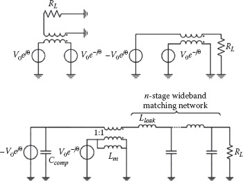
FIGURE 7.9 Two alternative options can be used to drive a single ended load from two single ended sources using a transformer (top left and right). The actual transformer-based combiner design includes the transformation and leak inductances in the analysis along with the output matching network (bottom).
The alternative transformer topology turns the single ended signal source into a floating signal source such that the two signal sources combined can feed a single ended load impedance. This approach turned out to be more promising even when including also the parasitic elements of the transformer in the analysis. For the final analysis, not only have the transformer’s magnetizing and leakage inductance been included but also a wideband matching network at the secondary side of the transformer (Figure 7.9, bottom). The leakage inductance in the equivalent circuit diagram is taken as the first reactive element of the matching network.
In order for the out-phasing transmitter concept to work properly, one of the sources needs an inductive compensation susceptance while the other requires a capacitive compensation component. The transformer magnetizing inductance can be used as the inductive compensation element, while the capacitive compensation element has to be added separately. It can be shown that the transformer’s transformation ratio must be equal to one for correct operation. In order to achieve this ratio, the primary inductance Lp and the secondary inductance Ls must satisfy the following equation:
with k being the coupling coefficient of the transformer. The secondary inductance Ls can be derived from this formula; the coupling coefficient k will be typically fixed for a given implementation technology and Lp is constrained by the required compensation susceptance. The resulting leakage inductance can then be calculated as follows:
In order to achieve broadband operation of the combiner, Lp must be small, and k should be close to one. The final transformer-based combiner design has been tested with a class-E power amplifier device built with NXP Semiconductors’ 65 nm CMOS technology and EDMOS devices. The series resonators for both class-E output stages are shifted to the secondary side of the combiner in series with the transformer leakage inductance. A two-stage wideband impedance matching network was also added to offer the correct load impedance to the active devices over a wide operating bandwidth. The transformer was implemented using a three-layer printed circuit board with minimum feature sizes of 100 μm. The transformer coupling coefficient is rather low at 55%; it is the main bandwidth limiting factor.
7.4.1.2 Measurement Results
The output power and drain efficiency values of the transformer-based power amplifier design have been tested under various driving conditions; the supply voltage has been 3.6 V. The peak output power of 33.9 dBm was measured at 700 MHz; the maximum power gain observed was 20.1 dB at the same frequency. The maximum drain efficiency for 10 dB power back-off was measured at 650 MHz and was better than 50%.
7.4.2 BROADBAND CLASS-E RF POWER AMPLIFIER
Cellular network operators have a clear preference for flexible radio solutions. They would like to use as few different components in their system deployment as possible. From an RF power amplifier design point of view, this translates into a requirement for flexibility in operating frequencies and supported modulation schemes while maintaining high DC efficiency levels. A class-E RF power amplifier can serve as a building block for a variety of different cellular standards and modulation schemes. The challenge in designing a class-E power amplifier for broadband operation lies in the requirement for high efficiency and flat RF output power over a relatively large output frequency range.
In the analytical model used in the design of the amplifier, the active device is replaced by a switch with resistance values of Ron and Roff for the on and off states of the switch, respectively [15, 16]. The analysis further considers the DC feed inductance L, the loaded quality factor of the output tank circuit Q0, and operating mode (see Figure 7.10). Suboptimum class-E variable voltage operation (EVV operation) and nonzero switching voltage and zero switching slope have been chosen in order to reduce the peak voltage across the transistor terminals and to protect from over-voltage conditions. For class-EVV operation, at the switching time T, the following conditions must be met for the voltage VC(t) across the switch:
with α VDD being the voltage across the switch at the moment in time when the switch is closed (i.e., t = T = 1 ∕ fo). The peak voltage across the switch can decrease from 3.6 VDD to 2.5 VDD when α increases from α = 0, which corresponds to the ideal class-E operation, to α = 2 for certain nonideal switch, on-resistance Ron, as shown in Figure 7.10 (bottom). This indicates that class-EVV operation will lead to lower peak voltage across the switch and as a result the power amplifier can use a higher supply voltage and thus deliver more RF output power at the cost of a slight decrease in efficiency.
The power output stage of the amplifier is designed using a single, extended drain, thick oxide NMOS transistor device implemented in 65 nm CMOS technology. It achieves an off-state breakdown voltage of 15 V. The output transistor is actually built using an array of smaller unit cell transistors; the total gate width of the transistor is 3.84 mm, and the channel length is 0.28 μm. This leads to an on-resistance Ron of 0.7 Ω, an off-resistance Roff of 10 kΩ, and a total off-state output capacitance of 4.14 pF. The square wave signal required to drive and operate the transistor as a switch is generated by an inverter-based driver implemented using standard thick-oxide MOS devices with a gate length of 0.28 μm. With proper biasing and a 2.4 V supply voltage, the driver stage can deliver a 2.4 Vpp square wave signal to the EDMOS output device.
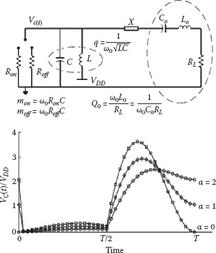
FIGURE 7.10 Schematic diagram of the analytical model used in the analysis and optimization of the class-E RF power amplifier (top). The timing diagram at the bottom shows the trace of the drain voltage of the transistor VDD over time normalized to the supply voltage for various values of the parameter a. After time T, the cycle repeats again.
With the desired target output power of 30 dBm at 1 GHz and 5 V supply voltage and the switch parameters as indicated previously, we can move on to determine the remaining values of the class-E circuit elements. In simulations it was found that for values α > 1.5, the peak voltage VDS across the EDMOS transistor is less than its breakdown voltage. We also noticed that the highest drain efficiency is not obtained for α = 0, the ideal class-E case, due to higher switching losses under this condition. In this design, α = 1.5 was chosen as an optimum compromise between output power, drain efficiency, and peak source drain voltage VDS. The corresponding optimum output load impedances for the fundamental (Z1,opt) and second harmonic (Z2,opt) output frequency were found to be
With these values as a starting point, the design of the two-stage LC-ladder matching network is relatively straightforward. The matching network needs to provide the desired load impedances from a 50 Ω termination within the frequency range of interest. During the optimization process more emphasis was put on a flat magnitude response for the fundamental frequency than a flat phase response.
7.4.2.1 Measurement Results
For test and measurement purposes the CMOS power amplifier chip was mounted on a printed circuit board made from Rogers substrate with εr = 3.5 and a thickness of 0.203 mm. The bond wires used to connect the chip to the substrate were kept as short as possible in order to keep their influence on the load impedances limited. The measurements were taken with a supply voltage of 5 V for the EDMOS output stage and 2.4 V for the driver stage.
In the frequency range between 550 and 1050 MHz a flat characteristic was measured for the available RF output power at a value of 30.5 dBm ± 0.5 dBm (see Figure 7.11). A power gain of about 16.5 dB was measured over the same frequency range. The drain efficiency and PAE remain above 67% and 52%, respectively, across the same bandwidth. The peak drain efficiency of 77% and peak PAE of 65% were observed at an operating frequency of 700 MHz and 31 dBm output power.
The class-E RF power amplifier can also be used as part of a polar transmitter architecture. In this case the drain efficiency with a reasonable power back-off is more critical. To enable output power control of the class-E amplifier and to improve its PAE at power back-off, supply voltage modulation has been applied. A power added efficiency of 45% and a drain efficiency of 68% were achieved with 10 dB power back-off from the reference of 30.2 dBm at 900 MHz operating frequency.
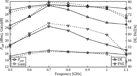
FIGURE 7.11 The class-E RF power amplifier can deliver about 30 dBm of output power over a wide operating frequency range. The drain efficiency and power added efficiency remain above 67% and 52%, respectively, over a frequency range of 550 to 1050 MHz.
We have presented several silicon-based solutions for large signal and small signal building blocks aimed at cellular infrastructure applications. They replace the more conventional GaAs technology-based designs except for the GaN transistors used for efficiency reasons in RF power amplifiers. These solutions can be seen as a first step toward further integration of the radio components in a cellular base station. The demonstrated measurement results can match up with state of the art in III-V compound technology solutions, but offer lower cost, higher level of integration, and additional features such as ESD robustness, calibration, and reconfigurability over a broad range of operating frequencies. The out-phasing RF power amplifier approach allows one to achieve high levels of DC power efficiency over a broad range of RF output power levels and operating frequencies. This enables the step up toward next generation cellular technologies such as LTE and phased array antenna approaches.
1. Avago Technologies, MGA-631P8. Low noise, high linearity, active bias low noise amplifier. Data sheet.
2. T. Chong et al., Design and performance of a 1.6–2.2 GHz low-noise high gain dual amplifier in GaAs e-pHEMT. Proceedings APMC, pp. 1–4, 2005.
3. O. Boric-Lucbeke et al., Si-MMIC BiCMOS low-noise high linearity amplifiers for base-station applications. Proceedings Asia-Pacific Microwave Conference, pp. 181–184, 2000.
4. V. Aparin et al., Highly linear SiGe BiCMOS LNA and mixer for cellular CDMA/AMPS applications. Proceedings RFIC, pp. 129–132, 2002.
5. L. Belostotski, J. W. Haslett, Sub-0.2 dB noise figure wideband room temperature CMOS LNA with non-50 ohm signal source impedance. IEEE Solid State Circuits, vol. 42, pp. 2492–2502, 2007.
6. D. Leenaerts, J. Bergervoet, J-W. Lobeek, M. Schmidt-Szalowski, 900 MHz/1800 MHz GSM base station LNA with sub-1 dB noise figure and +36 dBm OIP3. IEEE RFIC Symposium, pp. 513–516, 2010.
7. H. Chireix, High power out-phasing modulation. Proceedings of the IRE, pp. 1370–1392, Nov. 1935.
8. M. P. van der Heijden, M. Acar, J. S. Vromans, D. A. Calvillo-Cortes, A 19 W high-efficiency wide-band CMOS-GaN class-E Chireix RF out-phasing power amplifier. IEEE MTT-S Symposium, 2011.
9. J. Sonsky, A. Heringa, J. Perez-Gonzales, J. Benson, P. Chiang, S. Bardy, I. Volokhine, Innovative high voltage transistors for complex HV/RF SoCs in baseline CMOS. Proceedings International Symposium on VLSI Technology, Systems and Applications, 2008.
10. M. van Schie, M. van der Heijden, M. Acar, A. de Graauw, L. de Vreede, Analysis and design of a wideband high efficiency CMOS out-phasing amplifier. Proceedings 2010 IEEE Radio Frequency Integrated Circuits Symposium, p. 399 ff., 2010.
11. B. Serneels et al., A high-voltage ouput driver in a standard 2.5 V 0.25 μm CMOS technology. Digest of Technical Papers, International Solid State Circuits Conference, Feb. 2004.
12. S. Heck et al., A switching mode amplifier for class-S transmitters for clock frequencies up to 7.5 GHz in 0.25 μm SiGe BiCMOS. Digest IEEE RFIC Symposium, May 2010.
13. M. J. Pelk et al., A high-efficiency 100-W GaN three-way Doherty amplifier for base station applications. IEEE Transactions on Microwave Theory and Technology, vol. 56, no. 7, pp. 1528–1591, July 2008.
14. J. R. Long, Monolithic transformers for silicon RF IC design. IEEE Journal of Solid State Circuits, vol. 53, Sept. 2000.
15. M. Acar, A. Annema, B. Nauta, Variable-voltage class-E power amplifiers. Digest IEEE MTT-S International Microwave Symposium, pp. 1095–1098, June 2007.
16. R. Zhang, M. Acar, M. van der Heijden, M. Apostolidou, L. de Vreede, D. Leenaerts, A 500–1050 MHz +30 dBm class-E power amplifier in 65 nm CMOS. IEEE RFIC Symposium, 2011.
17. D. Calvillo-Cortes, M. Acar, M. van der Heijden, M. Apostolidou, L. de Vreede, J. Sonsky, A 65 nm CMOS pulse-width-controlled driver with 8 Vpp output voltage for switch-mode RF paths up to 3.6 GHz. Proceedings IEEE International Solid States Circuits Conference, p. 12, 2011.