
CONTENTS
4.1 Bit Error Rate, Noise, Gain, and Nonlinearity
4.3.2 Special Case: Zero-IF Receiver and Worst-Case Nonlinearity
4.4 Sensitivity to Block-Level Performance
4.4.2 Special Case: Zero-IF Receiver and Worst-Case Nonlinearity
4.5.1 Constant-Sensitivity Approach
4.5.2 Reduced Second-Order Sensitivity Approach
4.7 Adjustment of Process Variation Impact
4.7.1 Tuneability in Different LNA Topologies
4.7.2 Tuneability in Other Stages
4.7.3 Overall Design Considerations
4.7.4 Correcting the Corner Performance
4.7.5 Layout Impact Approximated
The increasing demand for compactness and speed of digital circuits and the necessity of integration of the digital back end electronics with radio frequency front ends calls for exploiting deep submicron technologies in RF circuit design. However, scaling into the deep submicron regime, mainly in CMOS (complementary metal oxide semiconductor) technologies, accentuates the effect of process spread and mismatch on the fabrication yield [1]. Furthermore, design for manufacturability requires all manufacturing and process variations to be considered in the design procedure. Statistical circuit-level methods based on modeling data provided by fabrication foundries (e.g., Monte Carlo) are extensively used to evaluate the effect of process spread and are utilized by simulation tools to design circuits with the desired performance over the specified range of process variation [2]. However, most of these statistical methods are based on random variation of design variables, which need long simulation times for large-scale circuits, like a full receiver. Furthermore, as the size and complexity of designs are increased, less insight is obtained from these random statistical methods.
Recently, system-level design techniques have been developed to determine the specifications of individual blocks of a receiver for minimum overall power consumption and for a given noise and nonlinearity performance [3–4,5]. However, system-level design guidelines in the literature do not sufficiently address the sensitivity of the receiver to process variations. In this chapter, for a given required overall performance, the block-level budgeting is performed in such a way that the effect of process variation on the overall performance is minimized. A system-level sensitivity analysis is performed on a generic receiver that can pinpoint the sensitive building blocks and show how to reduce the overall sensitivity to the performance of individual building blocks. Based on the presented analysis, the optimum plan for block-level specifications in terms of sensitivity to variability of components can be determined.
In this chapter, each building block of the receiver is described by three process-sensitive parameters: noise, nonlinearity, and voltage gain. In our analysis these parameters are defined in a way that they include the loading effect of the preceding and following blocks; in other words, the parameters are determined when the block is inside the system. The sensitivity of the overall performance of the receiver to variations of noise, nonlinearity, and gain of building blocks is calculated. In fact, the variations of noise, nonlinearity, and gain of building blocks represent variations in any circuit-level or process-technology level parameter that can affect the goal function of the receiver (BER as defined in the next section). Therefore, the presented methods include all relevant sources of variability. Since the number of parameters is limited to three for each block, faster computations are possible. On the other hand, any part of the receiver that can be characterized by these three parameters can be identified as a building block in the analysis. Therefore, the analysis is flexible in defining the building blocks of the system. To guarantee passing the yield test for all interferers, this analysis is carried out for the specified worst-case interferer.
The presented methods can include RF circuits, analog baseband circuitry, and ADC in the analysis. They are generic and can be used for any circuit topology or process technology, but there are some limitations:
1. The presented methods are applicable to narrowband systems or to wideband systems, the noise, nonlinearity and gain of which can be represented by an equivalent value across the whole band of operation. Therefore, some types of filters or frequency-dependent components cannot be covered by this analysis.
2. The interferers are assumed either to be completely filtered or to be amplified by almost the same gain as the desired signal is amplified with.
3. The operation bandwidth of the components preceding the mixer is assumed to be narrow enough so that the harmonics of the local oscilator (LO) do not down-convert the noise of these components. In other words, only the fundamental harmonic of the LO down-converts the noise of the preceding stages of the mixer. This assumption allows using the Friis formula to calculate the noise figure of a cascade of stages including a zero-IF mixer. For nonzero-IF mixers, additional calculations are done to include the effect of image noise.
Performing the analysis on systems violating any of these limitations may invalidate the obtained results.
In Section 4.1, bit error rate (BER) is defined as the goal function of the receiver and is described as a function of total noise, total nonlinearity, and input impedance of the receiver (for the given type of modulation). In Section 4.2, the performance requirements of a typical 60 GHz receiver for indoor applications are described. Total noise and total nonlinearity are described as a function of block-level noise, nonlinearity, and gain in Section 4.3—providing a connection between BER and block-level performance parameters. In Section 4.4, the relationships derived in Sections 4.1 and 4.3 are used to determine the sensitivity of the overall performance of the receiver to the performance of the building blocks. It is shown that, for all blocks, the first-order sensitivity to the gain of the block can be nullified, whereas the sensitivity to noise and nonlinearity of all the blocks cannot be minimized simultaneously. In Section 4.5, different approaches to minimizing the sensitivities derived in Section 4.4 are investigated. In Section 4.6 the design of two 60 GHz receivers including and excluding the ADC is explored using different system-level design guidelines presented in this chapter.
4.1 BIT ERROR RATE, NOISE, GAIN, AND NONLINEARITY
Defined as the ratio of erroneous received bits to the total number of received bits, bit error rate (BER) is an essential performance measure for every receiver involved with digital data. The BER in a receiver is, for a given type of modulation, directly determined by the signal-to-noise-plus-distortion ratio (SNDR). Normally, one can determine the required SNDR for the desired BER by system-level simulation of the baseband demodulator. Having the required SNDR and the specified minimum detectable signal (MDS), the maximum total noise-plus-distortion (NPD) can be calculated by
(4.1) |
where NPD is in watts, MDS is in dBm, and SNDR is measured in decibels at the output of the receiver. NPD is selected as the goal function of our analysis and since it is defined as the sum of the noise and nonlinearity distortion, it can be described as a function of noise and nonlinearity by
NPD = NAntenna + Ni,tot + ∞∑q=2PIMDqi,tot |
(4.2) |
where NAntenna is the noise coming from the antenna, Ni,tot is the equivalent input-referred available noise power of the receiver, and PIMDqi,tot is the equivalent input-referred available power of in-band qth order intermodulation distortion due to an out-of-band interferer.
We have assumed that there is no correlation between noise and distortion and between distortion components of different orders. We have also assumed that the noise and distortion have equal influence on the BER. However, in general that is not the case and the influence of the distortion on the BER depends on many factors, such as the modulation type of the interferer. Therefore, if the modulation type is known, (4.2) should be modified in a way that reflects the weight of the distortion. As illustrated in Figure 4.1, a noisy and nonlinear circuit can be described by an ideal noiseless and linear circuit with equivalent noise and nonlinearity distortions referred to the input. In this case, as shown in Figure 4.1(b), input-referred noise and distortions are represented by voltage sources. This representation can also be applied to a zero-IF mixer by considering its RF port as the input and its IF port as the output. In order to describe NPD in terms of equivalent voltages, we need to convert the available power of noise and distortion in (4.2) to their equivalent voltages. This results in
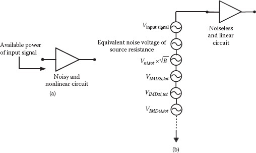
FIGURE 4.1 (a) A noisy and nonlinear circuit that can serve here both as the total receiver or one of its building blocks; (b) corresponding noiseless and linear circuit with equivalent noise and distortion voltage at input.
where
k = 1.38 × 10⁻²³ J/K is the Boltzmann constant
T is the absolute temperature
B is the effective noise bandwidth
Rin is the input impedance
Rs is the source impedance
Vni,tot is the equivalent input-referred noise voltage in V/√Hz
VIMDqi,tot is the equivalent input-referred voltage of qth order intermodulation distortion in volts, as shown in Figure 4.1(b)
Without loss of generality and for simplicity, the input impedance of the receiver is assumed to have only a real part.
Once the required Vni,tot and VIMDqi,tot of the whole receiver are determined, overall system specifications, including noise factor (NFtot) and the voltage of qth order input intercept point (VIPqi,tot), can be calculated:
NFtot = 4kT × Rs + ˉV2ni,tot(Rin + RsRin)24kT × Rs |
(4.4) |
1Vq−1IPqi,tot = VIMDqi,totVqinterferer |
(4.5) |
where Vinterferer is the worst-case out-of-band interferer signal voltage at the input. Substituting ViMDqi,tot from (4.5) in (4.3) yields the NPD as a function of VIPqi,tot and Vni,tot:
NPD = kTB + (Rs + Rin)24RsR2in × (BˉV2ni,tot + ∞∑q=2V2qinterfererV2q−2IPqi,tot) |
(4.6) |
The NPD can also be affected by IQ mismatch (only in receivers with I and Q paths) and phase noise. IQ phase or amplitude imbalance results in some cross talk between I and Q channels. This cross talk appears as a distortion and affects the NPD. Block-level budgeting of the noise, gain, and nonlinearity does not have a significant (if any) impact on the IQ mismatch. Therefore, if the amount of the IQ cross talk is known, its impact can be treated as a constant distortion added to the NPD and in this way it can be incorporated in the analysis. Extensive research has been done on IQ mismatch cancelation methods over the past years. Digital IQ imbalance compensation methods are widely used to suppress the impact of IQ mismatch. Details of these methods are beyond the scope of this chapter.
The phase noise originating from the frequency synthesizer can cause interchannel and in-band interference. The interchannel interference can be modeled as a distortion added to the NPD, assuming a worst-case adjacent-channel interference. However, the impact of in-band interference is signal dependent and cannot be modeled with just a constant additive distortion because the effect of phase noise is multiplicative and not additive, like thermal noise. Nevertheless, the impact of phase noise is hardly dependent on the noise, gain, and nonlinearity of the building blocks of the receiver. Therefore, the way the block-level budgeting is performed in the receiver can hardly influence the impact of the phase noise on the receiver performance. Minimization of the phase noise impact can be best accomplished in the frequency synthesizer section (e.g., phase-locked loop). In the rest of the chapter, the focus will be on the impact of the noise, gain, and nonlinearity distortion of individual blocks of the receiver on the NPD. Therefore, IQ mismatch and phase noise, which are rather independent of the block-level budgeting of the receiver, will not be addressed any further in this chapter.
The frequency band of 57–66 GHz, as allocated by the regulatory agencies in Europe, Japan, Canada, and the United States, can be used for high rate wireless personal area network (WPAN) applications [6]. According to the IEEE 802.15.3c standard, three different modes are possible for the physical layer of such a network: single-carrier mode, high speed interface mode, and audio/visual mode. The single-carrier mode supports various types of modulation schemes including π/2 QPSK, π/2 8-PSK, π/2 16-QAM, precode MSK, precoded GMSK, on/off keying (OOK), and dual alternate mark inversion (DAMI). The high speed interface mode is designed for non-line-of-sight operation and uses OFDM. The audio/visual mode is also designed for non-line-of-sight operation, uses OFDM, and is considered for uncompressed, high definition video and audio transport.
The whole band is divided into four channels with center frequencies located at 58.32, 60.480, 62.640, and 64.8 GHz, each with a bandwidth of 2.16 GHz [6]. A transceiver complying with the single-carrier mode should support at least one of these channels. A transceiver complying with the high speed interface mode should support at least the channel centered at 60.480 GHz or the one centered at 62.640 GHz. The audio/visual mode is in turn divided into two modes of low data rate (LRP: in the order of 5 Mbps) and high data rate (HRP: in the order of 1 Gbps). A transceiver complying with HRP mode should support at least the channel centered at 60.480 GHz. On the other hand, in the LRP mode, the bandwidth of the channels is about 98 MHz (i.e., in each of the mentioned channels, three LRP channels, with 98 MHz bandwidth, are defined around the center).
Different physical layer definitions are a result of different possible application demands. For example, a kiosk application would require 1.5 Gbps data rate at a 1 m range. This data rate at such a short range can be easily provided by the single-carrier mode with less complexity and thus lower cost compared to physical layer definitions, which use OFDM. On the other hand, the audio/visual mode is best fitted to uncompressed video streaming applications. An ad hoc system for connecting computers and devices around a conference table can be best implemented by the high speed interface mode because, in this case, all the devices in the WPAN are expected to have bidirectional, non-line-of-sight, high speed, low latency communication [6].
According to the IEEE 802.15.3c standard, the limit for effective isotropic radiated power (EIRP) at this frequency band is 27 dBi for indoors and 40 dBi for outdoors in the United States. The EIRP limit in Japan and Australia is 57 dBi and 51.8 dBi, respectively. It is worth remembering that EIRP is the sum of the transmitter output power and its antenna gain.
In the single-carrier mode, the frame error rate must be less than 8%, with a frame payload length of 2,048 octets. The minimum detectable signal varies between –70 and –46 dBm, depending on the data rate. The maximum tolerable power level of the incoming signal, which meets the required error rate, is –10 dBm.
In the high speed interface mode, for a BER of 10–6, the minimum detectable signal varies between –50 and –70 dBm, depending on the required data rate. The maximum tolerable power level of the incoming signal, which meets the required error rate, is –25 dBm.
In the audio/visual mode, a BER of less than 10–7 must be met with a bit stream generated by a special pseudorandom sequence defined in the standard. The audio/visual mode has two different data rate options: high data rate in the order of gigabits per second and low data rate in the order of megabits per second. For low data-rate and high data-rate applications, the minimum detectable signal of the receiver should be –70 and –50 dBm, respectively. The maximum tolerable power level of the incoming signal is –30 and –24 dBm for low data rate and high data rate modes, respectively.
To address the impact of block-level performance on the overall performance, we first start with a rather general case including the image noise and a precise calculation of the total nonlinearity and then we derive a more useful special case.
In this section the building blocks of the receiver are described with three parameters including noise, nonlinearity, and gain, as shown in Figure 4.2(a). The system consists of N stages with at least one mixer as the Lth stage. The gain of each stage is defined as the ratio between the output voltage and the input voltage of each stage when the stage is inside the system, as shown in Figure 4.2(b). The output noise voltage of each stage is observed by assuming that all the other stages and also the antenna are noiseless. Then the input noise voltage of the stage is calculated via dividing the output noise voltage by the gain, as shown in Figure 4.2(c). A similar procedure is used to define the nonlinearities of stages, as described later in more detail. The stages prior to the mixer are characterized by two additional parameters: Avn,k,image is the gain by which the noise voltage of the previous stage (the antenna in the case of k = 1) at the image band is amplified and Vnout,k,image is the noise at the output of the kth stage, generated by the stage itself, residing at the image band. Defining Vnout,k as the output noise of the kth stage, generated by the stage itself, Vni,k is defined as Vnout,k divided by voltage gain (Avn,k). In order to calculate the overall equivalent input-referred noise voltage (Vni,tot) as a function of the noise and gain of individual stages, the total noise at the output of the receiver, generated by the receiver itself (and not by the antenna), is expressed in (4.7).
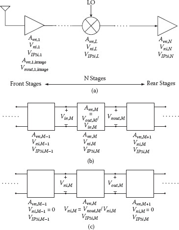
FIGURE 4.2 (a) N nonlinear and noisy stages cascaded in the receiver described by their noise, nonlinearity and gain. (b) Gain is defined as the ratio between the output voltage of the stage to its input voltage when the stage is in the system. (c) Noise of a stage is defined by assuming that all the other stages and antenna are noiseless and observing the noise voltage at the output of the stage.
The meanings of all parameters are described in Table 4.1. Two dummy variables—Avn,0 and Avn,N+1—are defined as unity to facilitate the representation of calculations:
Defining two auxiliary variables, as in (4.8) and (4.9); replacing Vnout,k with Vni,kAvn,k; and making some simplifications, the total input-referred noise of the receiver is obtained in (4.10).
cImN,k = ˉV2nout,k,imageˉV2nout,k |
(4.8) |
(4.9) |
TABLE 4.1
Some of the Notations Used in the Formulae
Notation for |
||
Parameter |
kth Stage |
Whole receiver |
Noise voltage at the output |
Vnout,k |
Vnout,tot |
Image noise voltage at the output |
Vnout,k,image |
Vnout,tot,image |
Gain: the ratio between output voltage and input voltage at the signal band |
Avn,k |
Avn,tot |
Image gain: the ratio between output voltage and input voltage at the image band |
Avn,k,image |
Avn,tot,image |
Equivalent input-referred noise voltage |
Vni,k = Vnout,kAvn,k |
Vni,tot = Vnout,totAvn,tot |
For obtaining (4.10), the relationship between the effective noise bandwidth (B) in (4.6) and the signal bandwidth (Bsig) is defined as follows:
(4.11) |
The contribution of the kth stage to the total noise is calculated from
This means that the noise contribution of each stage is inversely proportional to the square of the voltage gain of its preceding stages.
In order to calculate the overall voltage of the qth order input intercept point of the receiver (VIPqi,tot) in terms of that of the individual stages, the phase relationships between the nonlinearities and the gains of the stages must be introduced into the calculations.
To start the analysis, the nonlinearity and gain parameters of the receiver and its stages are expressed in phasor form, as shown in Table 4.2. The total input-referred voltage of the qth order intermodulation distortion can be expressed in terms of the distortion of the individual stages by
VIMDqi,tot∠φIMDqi,tot = N∑k=1VIMDqi,k∠φIMDqi,kk−1∏j=0Avn,j∠qφvn,j |
(4.13) |
Then the distortions can be expressed in terms of intercept points:
VIMDqi,k∠φIMDqi,k = Vqinterferer × k−1∏j=0Aq−1vn,j∠qφvn,jVq − 1IPqi,k∠(q − 1)φIPqi,k |
(4.14) |
TABLE 4.2
Some of the Notations in Phasor Form
Phasor notation for |
||
Parameter |
kth Stage |
Whole receiver |
Input-referred voltage of the qth order intermodulation distortion |
VIMDqi,k < ϕIMDqi,k |
VIMDqi,tot < ϕIMDqi,tot |
Voltage of the qth order input intercept point |
VIPqi,k < ϕIPqi,k |
VIPqi,tot < ϕIPqi,tot |
Voltage gain including the loading effect |
Avn,k < ϕvn,k |
Avn,tot < ϕvn,tot |
Therefore, the total intercept point can be expressed in terms of the intercept points of the individual stages by substituting the distortions from (4.14) into (4.13):
or
4.3.2 SPECIAL CASE: ZERO-IF RECEIVER AND WORST-CASE NONLINEARITY
In the special case of a zero-IF receiver with worst-case nonlinearity superposition, the preceding relationships can be simplified substantially. This special case is the focus of most of the analysis in the rest of this work.
In a zero-IF mixer with a complex mixer and I/Q signal paths, (4.10)–(4.12) simplify to (4.17)–(4.19):
ˉV2ni,tot = N∑k=1ˉV2ni,kk−1∏j=0A2vn,j |
(4.17) |
(4.18) |
CNoise(k) = ˉV2ni,kk−1∏j=0A2vn,j |
(4.19) |
If the intermodulation distortions of the consecutive stages are added in-phase, resulting in a worst-case scenario, the expression for the intercept point in (4.15) simplifies to [3]
1Vq−1IPqi,tot = N∑k=1k−1∏j=0Aq−1vn,jVq−1IPqi,k |
(4.20) |
The preceding relationships are based on the assumption that the interferer and the in-band signal are amplified with almost the same gain. However, if the interferer is far from the in-band signal in the frequency domain, it can be filtered at the input of the receiver such that it generates no distortion.
Based on (4.20), the contribution of the kth stage to the total qth order nonlinearity distortion is equal to
CDistortion,q(k) = k−1∏j=0Aq−1vn,jVq−1IPqi,k |
(4.21) |
This means that the nonlinearity distortion contribution of each stage is directly proportional to the combined voltage gain of its preceding stages. This in fact creates a trade-off in defining the gain of stages. The parameters CNoise and CDistortion will play a central role in the rest of our analysis.
4.4 SENSITIVITY TO BLOCK-LEVEL PERFORMANCE
In analogy with the previous section, the sensitivities of the overall performance to the block-level performance are calculated in both general and specific cases.
To find a block-level budgeting for optimum robustness of the receiver to variability of block-level performance, one has to minimize the sensitivity of the total performance to the performance of individual blocks. In fact, one way to make the receiver robust to process variations is to make it robust to performance degradations of its building blocks. In this section, the sensitivity of total NPD to the noise, nonlinearity, and gain of individual blocks is calculated. The normalized single-point sensitivity of F(x) to the variable x is defined by the following operator [2]:
(4.22) |
This should be calculated at the selected nominal values of x and F(x). As mentioned earlier, to achieve a certain BER, a specific NPD requirement has to be met. Therefore, variations of NPD can cause variations in BER. The variations of NPD can be described as a function of the variation of the performance parameters of the individual stages:
The random variables ΔAvn,k, ΔVni,k, ΔVIPqi,k, and ΔZin, which represent the performance variations of the individual stages and the input impedance, are usually correlated. However, regardless of the amount of correlation between these random variables, one can minimize ΔNPD by minimizing (ideally, nullifying) the derivatives in (4.23), which are proportional to the sensitivity functions. Furthermore, the random variables ΔAvn,k, ΔVni,k, and ΔVIPqi,k are in general different for different stages (i.e., different values of k). If they are significantly larger for a specific stage, it is advisable to focus on reducing the sensitivity of the total performance to the performance of that stage. However, such knowledge requires circuit-level information about each stage, which may be achieved during the circuit design. Therefore, in this analysis, we attempt to reduce all the sensitivities, assuming that the random variables ΔAvn,k, ΔVni,k, and ΔVIPqi,k are in the same order for different stages. The sensitivity functions of NPD to performance parameters of each stage (Vni,k, VIPqi,k, and Avn,k) are listed in (4.25), (4.26), and (4.27), respectively. The derivatives are taken using the chain rule applied to (4.6), (4.10), and (4.16). To simplify the equations, an auxiliary variable is defined in the following:
(4.24) |
It is clear from (4.25)–(4.27) that the sensitivities to the noise and nonlinearity of the stages cannot be made zero, whereas the sensitivity to the gain of individual stages can be made zero.
4.4.2 SPECIAL CASE: ZERO-IF RECEIVER AND WORST-CASE NONLINEARITY
If the receiver is zero-IF with a complex mixer and I/Q signal paths in IF and the design is done for worst-case scenario, in which the intermodulation distortions of the individual stages are assumed to add up in phase, (4.25)–(4.27) are simplified to (4.28)–(4.30):
SNPDˉV2ni,k = BReq × NPD × ˉV2ni,kk−1∏j=0A2vn,j |
(4.28) |
SNPD(1Vq−1IPqi,k) = 2V2qinterfererReq × Vq−1IPqi,tot × NPD × k−1∏j=0Aq−1vn,jVq−1IPqi,k |
(4.29) |
The second-order sensitivity of NPD to block-level gain is proportional to the second-order derivative of NPD with respect to block-level gains as described in (4.31) and (4.32):
∂2NPD∂A2vn,k = 2R−1eqA2vn,k × (∞∑q=2(V2qinterferer((q − 1)2(N∑j=k+1j−1∏m=1Aq−1vn,mVq−1IPqi,j)2 + (q −1)(q −2)Vq−1IPqi,tot × N∑j=k+1j−1∏m=1Aq−1vn,mVq−1IPqi,j)) + 3 N∑j=k+1BˉV2ni,jj−1∏m=1A2vn,m) |
(4.32) |
These are valid for (1 ≤ k < N).
An inspection of (4.19) and (4.28) and, in the general case, (4.12) and (4.25) shows that the sensitivity to the noise performance of each stage is proportional to its contribution to the total noise of the receiver. A similar inspection of (4.21) and (4.29) reveals that the sensitivity to the qth order nonlinearity of each component is proportional to its contribution to the total qth order nonlinearity. Therefore, for a given total noise and total nonlinearity, reducing the sensitivity to noise/nonlinearity of one stage results in increased sensitivity to noise/nonlinearity of other stages. On the other hand, the sensitivity to gain of each block can be set to zero as implied by (4.27) or (4.30). Furthermore, according to (4.31) and (4.32), the second-order sensitivity to block-level gains cannot be nullified, but can be reduced by lowering the contribution of the rear stages to the total noise and nonlinearity.
One solution for zeroing the first order sensitivity of NPD to gains in (4.30) is
(4.33) |
(4.34) |
(4.35) |
where αk (1 ≤ k < N) is a parameter that must be chosen by the designer; we call it contribution factor of a stage, because it determines the ratio of the noise and nonlinearity distortion contribution of each stage to that of its following stage. To nullify (4.30) for every stage, (4.33)–(4.35) must be satisfied for (1 < k ≤ N). In case of dominance of third-order nonlinearity, (4.35) simplifies to
(4.36) |
which means that the third-order intermodulation distortion must be 3 dB below the level of the noise coming from the receiver itself.
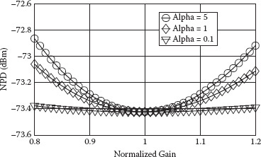
FIGURE 4.3 NPD versus normalized variation of the gain of the first stage for different values of α.
According to (4.31) and (4.32), the second-order sensitivity of NPD to the gain of front stages is bigger than that of rear stages. For a system that satisfies (4.33)–(4.35), the reduction of the second-order sensitivity to the gain of front stages requires their α to be smaller than unity, resulting in a lower contribution of rear stages to total noise and nonlinearity. In fact, if α is smaller than unity for every stage, the contribution of each stage to the total noise and nonlinearity, as quantified by (4.12), (4.19), and (4.21), will be smaller than that of its previous stage. It is worth mentioning that a higher contribution of a stage to the total noise (or nonlinearity distortion) does not necessarily mean that it is noisier (or more nonlinear), because the contribution of one stage to total noise (or total nonlinearity distortion) is not only a function of the noise (or nonlinearity) of the stage itself but also a function of the gain of its previous stages, as described by (4.12), (4.19), and (4.21). Figure 4.3 shows the NPD of a receiver as a function of the gain of its first stage (normalized to its nominal value) for different values of α. It shows the significant impact of α on the second-order sensitivity, with smaller values of α yielding smaller second-order sensitivity to the gain of the LNA.
The equations derived in Section 4.4 are insightful for both analysis and synthesis of a receiver. From the analysis perspective, they can determine the most sensitive building blocks of the receiver. From the synthesis perspective, they can be used to develop design approaches for minimum sensitivity to variability of building blocks. In this section, three design approaches are investigated. In all of them, the firstorder sensitivity of the NPD to the gain of each block is set to zero. The difference between the three methods is in the different values chosen for α.
In the first approach, the sensitivities of the NPD to the noise and nonlinearity of the individual stages are all the same, while the sensitivity of the NPD to the gain of each block is set to zero by setting α to one. In the second approach, the second-order sensitivity to the gain of building blocks is reduced, while the first-order sensitivity to gain is kept at zero, by keeping α smaller than one. In the third approach, an optimum-power design method is described [3] and the first-order sensitivity to the gain of building blocks is set to zero by adding a new condition to the method; in this method, α is a function of the power consumption of the components. All the approaches are presented for the special case of the zero-IF receiver with a worst-case nonlinearity scenario, although they have the potential to be generalized to other receiver architectures and scenarios.
4.5.1 CONSTANT-SENSITIVITY APPROACH
For a given total noise and total nonlinearity, reducing the sensitivity to noise/non-linearity of one stage results in increased sensitivity to noise/nonlinearity of other stages, because reducing the contribution of one stage to total noise or nonlinearity, (4.19) and (4.21), increases the contribution of other stages. As a result, by keeping sensitivities equal for all the stages, one can avoid extra-sensitive nodes in the receiver. Forcing the sensitivity to noise in (4.28) to be equal for all k (1 ≤ k ≤ N) and using (4.17) and (4.19) yields
(4.37) |
This means that the input-referred noise voltage of each stage must be better than that of its following stage by a factor of its voltage gain:
(4.38) |
Forcing the sensitivity to nonlinearity in (4.29) to be constant for all k (1 ≤ k ≤ N) and using (4.20) and (4.21) yields
CDistortion,q(k) = k−1∏j=0Aq−1vn,jVq−1IPqi,k = 1N × Vq−1IPqi,tot |
(4.39) |
This means that the qth order nonlinearity performance of each stage must be better than that of its preceding stage by a factor of voltage gain of its preceding stage:
(4.40) |
In the constant-sensitivity approach, (4.37) and (4.39) guarantee that the sensitivity to noise and nonlinearity of all the stages is the same and the contribution of all the stages to total noise and nonlinearity is equal.
According to (4.38) and (4.40) two conditions for zeroing the first-order sensitivity of NPD to the gain, (4.33) and (4.34), are automatically satisfied in this approach with α equal to unity for all the stages. Consequently, the designer has to satisfy (4.35) to nullify the first-order sensitivity to the gain.
Therefore, in this approach, first-order sensitivity to gain of each stage is set to zero and the sensitivity to noise and nonlinearity of all stages is equal.
4.5.2 REDUCED SECOND-ORDER SENSITIVITY APPROACH
In this approach, in addition to nullifying the first-order sensitivity to block-level gains in (4.30), the second-order sensitivity to the gain of front stages in (4.31) and (4.32) is reduced. To achieve that, α must be smaller than unity for every stage, resulting in
(4.41) |
(4.42) |
In contrast to the constant-sensitivity approach, in the reduced second-order sensitivity approach there is no unique solution for zeroing (4.30); that is, choosing any α smaller than unity is sufficient. In fact, making α smaller for each stage can further reduce the value of the second-order sensitivity to the gain of that stage. Theoretically, there is no lower limit for α and setting α to zero yields the lowest second-order sensitivity; however, in practice, obtaining very low values of α is difficult because it demands highly linear and low noise components, which are either impractical to implement or entail extremely high power consumptions.
In this approach, more attention is paid to the sensitivity of the NPD to the gain of individual blocks and no constraints are defined for sensitivity to the noise and nonlinearity of building blocks, because reducing the sensitivity of the NPD to the noise or nonlinearity of one stage increases the sensitivity of the NPD to the noise and nonlinearity of other stages, as described in the preceding subsection. Therefore, the overall impact of adjusting the sensitivities to block-level noise and nonlinearity on the robustness is not expected to be significant. Consequently, the reduced second-order sensitivity approach is expected to provide more robustness to process variations as compared to the constant-sensitivity approach.
As a side effect of reducing the second-order sensitivity of the NPD to the gain of the stages, the sensitivity to noise and nonlinearity of front stages (such as LNA) is increased in this approach, whereas the sensitivity to noise and nonlinearity of rear stages (like baseband filters) is reduced.
In optimum-power design, as suggested in reference 3, a linear relationship is assumed between power consumption and dynamic range of the components:
(4.43) |
where P is the power consumption of the component and PC is the proportionality constant and is called power coefficient.
This assumption is valid in many RF components in specific operating regions [3]. Therefore, the resulting method is applicable solely in those regions. In this thesis, the optimum-power method is used as a means of comparison with the methods developed in this work so that we can verify that the methods aiming at robustness may also satisfy the requirements of optimum-power design. Optimum-power methodology proposes a block-level budgeting plan, which results in minimum power consumption for a given total noise and nonlinearity requirement [3]:
CNoise(k) = ˉV2ni,kk−1∏j=0A2vn,j = ˉV2ni,tot × 3√PCkN∑m=13√PCm |
(4.44) |
CDistortion,3(k) = k−1∏j=0A2vn,jV2IP3i,k = 1V2IP3i,tot × 3√PCkN∑m=13√PCm |
(4.45) |
where PCk is the power coefficient of the kth stage and the total power consumption after optimization is obtained from (4.46). In this approach, third-order nonlinearity is assumed to be the dominant source of distortion and the other orders of nonlinearity are neglected.
(4.46) |
In the special case that the power coefficients of all blocks are equal, (4.44) and (4.45) simplify to (4.37) and (4.39), respectively, and the optimum-power design gives the same results as the constant-sensitivity design.
However, the guideline proposed in reference 3 does not determine the total noise and total nonlinearity of the receiver. As was mentioned in Section 4.1, the required BER determines the required noise plus distortion (NPD) but does not specify the contribution of the noise or nonlinearity to the total NPD. Thus, the designer needs to specify VIP3i,tot and Vni,tot in such a way that the total power consumption in (4.46) is minimized and the required NPD in (4.3) is satisfied. It can be proven that minimum power is achieved when the condition of (4.36) is met.
An inspection of (4.44)–(4.45) reveals that in this approach the noise and nonlinearity of consecutive stages have the following relationships:
(4.47) |
(4.48) |
This means that this approach also satisfies the first two conditions for zeroing the first-order sensitivity of NPD to the gain of stages as described in (4.33)–(4.34) and α is equal to the third root of the ratio of the power coefficients. Therefore, satisfying (4.36) is also necessary for zeroing the first-order sensitivity to the gains. Thus, selecting the total noise and nonlinearity of the receiver for minimum power leads to the nullification of the first-order sensitivity of NPD to block-level gains. This is an important advantage of the optimum-power design.
Based on (4.44) and (4.45), and (4.28) and (4.29), the sensitivity to the noise and nonlinearity of each block is directly proportional to the third root of its power coefficient—meaning that the overall system performance is more sensitive to power-hungry blocks.
In the rest of the chapter, the optimum-power approach refers to the herewith modified version of the method introduced in reference 3, which also satisfies the condition of (4.36).
In the course of development of this method, it is assumed that the noise and nonlinearity performance of an RF circuit can be improved linearly and indefinitely by just increasing the power consumption and that, for constant power consumption, the noise and linearity performance can be traded for each other [3]. Due to the limited range of validity of these assumptions, the method should be used with caution.
The three approaches studied in this section are summarized in Table 4.3. Clearly, these approaches should be compared when their specified NPDs are equal. According to the second and last row of the table, the optimum-power design only satisfies the necessary conditions for reduced second-order sensitivity design if the power coefficients of the rear stages are smaller than those of the front stages. Alternatively, the optimum-power design only gives the same specifications of the constant-sensitivity approach if the power coefficients of all the stages are equal.
In the special case that the power coefficient of each block is smaller than that of its previous stage, the α of the optimum-power design is smaller than unity and the optimum-power design meets the conditions of the reduced second-order sensitivity approach. Accordingly, the second-order sensitivity of the NPD to the gain of a stage is higher if its following stages have larger power coefficients because, in optimum-power design, the blocks with larger power coefficients have higher contribution to the total noise (CNoise) and nonlinearity distortion (CDistortion); this can be verified by inspection of (4.19) and (4.21) and (4.47)–(4.48). In other words, for a stage followed by another one with a larger power coefficient, the value of α is larger than unity, contradicting the requirements of the reduced second-order sensitivity approach. In fact, optimum-power design does not put any constraint on the position of large-power coefficient blocks, but having this sort of block at the front stages of the receiver would let the optimum-power design produce the same specifications as suggested by the reduced second-order sensitivity approach.
TABLE 4.3
Summary of the Three Explained Approaches
Constant sensitivity |
Reduced second-order sensitivity |
Optimum power |
|
Contribution factor (αk) |
= 1 |
<1 |
=3√PCk+13√PCk |
First-order sensitivity to the gain of stages |
0 |
0 |
0 |
Second-order sensitivity to the gain of front stages |
High |
Low |
High if rear stages are power hungry; low if rear stages are low power |
Sensitivity to noise and nonlinearity of each stage |
Constant |
High for front stages; low for rear stages |
Proportional to third root of power coefficient |
As a conclusion, the reduced second-order sensitivity approach is the ideal solution in terms of improving the robustness of a receiver to process variations. However, it is not always a practical solution, considering its implications for the power consumption. If the large-power coefficient blocks are located in the front stages of the receiver, the reduced second-order sensitivity approach can be used without excessive increase in the power consumption. However, if the large-power coefficient blocks are in the rear stages of the receiver, the optimum-power method is preferred as it meets the requirement for zeroing the first-order sensitivity to the gain of all the stages while yielding the minimum power consumption.
In this section we apply the design approaches described in Section 4.2.5 to 60 GHz zero-IF receivers. First, we investigate the case of a receiver without analog-to-digital converter (ADC) and then we study another receiver that includes an ADC.
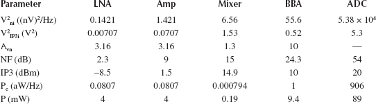
The ADC-less 60 GHz zero-IF receiver shown in Figure 4.4 is considered to perform a comparison between different design approaches. A nonoptimum design based on a tested 60 GHz LNA and mixer is also included in the comparison. The power coefficients, used to estimate the power consumption in each case, and the block-level gains are extracted from simulated and measured circuits [7,8]. The requirements of the overall system are an SNDR of 12 dB and an MDS of –61.4 dBm, which result in an NPD of –73.4 dBm. The tolerable interference power at the input of the receiver is –33 dBm and the RF bandwidth is 2 GHz. For the sake of practicality, these requirements are based on state-of-the-art 60 GHz receivers [9]. Assuming that third-order intermodulation distortions are the dominant part of nonlinearities, (4.36), (4.3), (4.4), and (4.5) can be used to find the required noise figure and IIP3, which are 6 dB and –10 dBm, respectively. Block-level specifications obtained from each of the four design approaches are listed in Table 4.4. The input impedance of the receiver is assumed to be 50 Ω for all cases. All four designs satisfy the noise figure and IP3 requirements. The power consumption is estimated by [3]
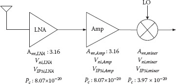
FIGURE 4.4 Three-stage ADC-less receiver used in the case study.
(4.49) |
The variation of NPD as a function of the variations in the gain of the LNA, for the four approaches, is illustrated in Figure 4.5. The gain of the LNA is varied by ±20% around its nominal value.
Except for the nonoptimum design, all the approaches result in zero first-order sensitivity of the NPD to the gain of the LNA, whereas the reduced second-order sensitivity design shows minimum variation of NPD with respect to gain deviations in the LNA. In this example the second-order sensitivity to gain in optimum-power design is not much higher than the one in the reduced second-order sensitivity approach because the power coefficient of the final stage is very low and therefore its noise and nonlinearity contribution are low. Please note that because only the gain of one stage is varied in Figure 4.6, the variations of NPD are small. The value of α in the case of reduced second-order sensitivity approach is 0.43. If smaller values of α could be obtained, smaller second-order sensitivities would be possible.
TABLE 4.4
Block-Level Specifications of the Four Design Approaches
Parameter |
Constant sensitivity |
Reduced second-order sensitivity |
Optimum power |
Nonoptimum |
V2ni,LNA (V2/Hz) |
2.06 × 10⁻¹⁹ |
3.599 × 10⁻¹⁹ |
2.6 × 10⁻¹⁹ |
2.896 × 10⁻¹⁹ |
V2ni,Amp (V2/Hz) |
2.06 × 10⁻¹⁸ |
1.542 × 10⁻¹⁸ |
2.6 × 10⁻¹⁸ |
1.274 × 10⁻¹⁸ |
V2ni,Mixer (V2/Hz) |
2.06 × 10⁻¹⁷ |
1.028 × 10⁻¹⁷ |
9.56 × 10⁻¹⁸ |
1.995 × 10⁻¹⁷ |
V2IP3i,LNA (V2) |
0.015 |
0.0086 |
0.0118 |
0.1256 |
V2IP3i,Amp (V2) |
0.15 |
0.2000 |
0.118 |
0.32 |
V2IP3i,Mixer (V2) |
1.5 |
3.0001 |
3.2 |
0.621 |
Estimated power (mW) |
12 |
13.6 |
8.6 |
55 |
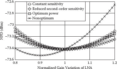
FIGURE 4.5 NPD versus normalized variation of LNA gain for the four different designs.
In Figure 4.7 and Figure 4.8 the statistical behavior of the four designs of Table 4.4 is compared. Noise, linearity, and gain of all the stages are randomly changed in an interval of ±20% from their nominal values. Using MATLAB, half a million samples are made in this way for each design and the NPD of each sample is calculated.
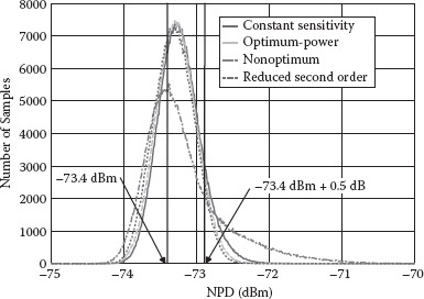
FIGURE 4.6 Comparing the four different designs in terms of number of random samples versus NPD.
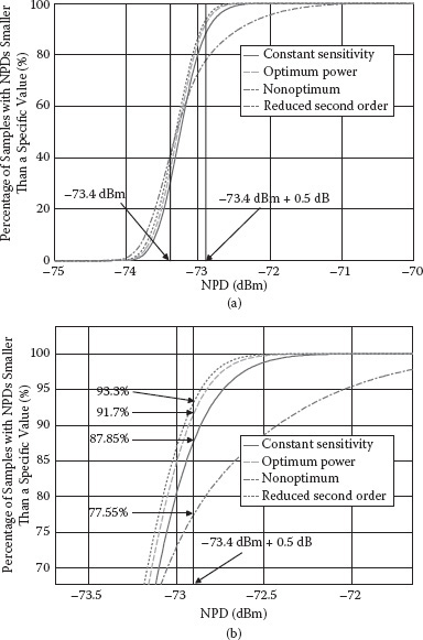
FIGURE 4.7 Comparing the four different designs in terms of (a) percentage of random samples with smaller than a specific NPD; (b) zoomed view of (a).
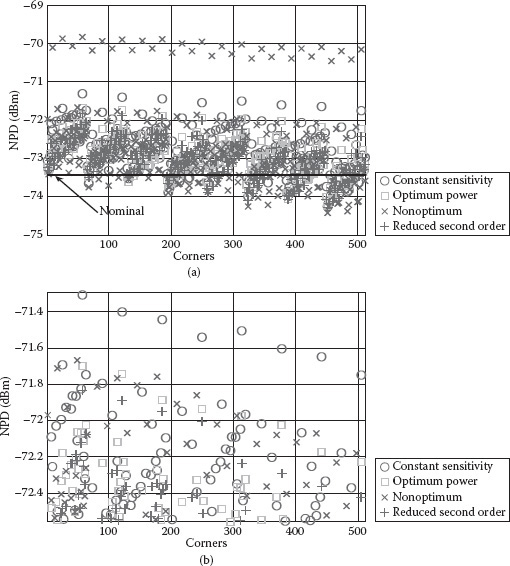
FIGURE 4.8 (a) NPDs of designs of Table 4.3 on the corners of the parameter space; (b) zoomed view.
The range of NPDs between –72 and –68 dBm is divided into intervals of 0.01 dB and the number of samples falling in each interval is shown in Figure 4.7. The non-optimum design clearly shows the highest number of out-of-specification samples, whereas reduced second-order sensitivity design shows the lowest number of out-of-specification samples. Figure 4.7 shows the percentage of samples with NPDs smaller than a specific value. For instance the percentage of samples with NPDs more than 0.5 dB higher than nominal is 12.15%, 8.3%, 22.45%, and 6.7% for constant sensitivity, optimum-power, nonoptimum, and reduced second-order sensitivity designs, respectively. The percentage of samples with NPDs more than 1 dB higher than nominal is 0.59%, 0.09%, 9.58%, and 0.03% for the aforementioned designs respectively. The reduced second-order design achieves 99.9% yield if the acceptable limit for NPD is set to –72.5 dBm, whereas the nonoptimum design achieves such yield if that limit is set to –70.7 dBm. If one decides to compensate for this difference by overdesigning the nonoptimum case, one has to shift the nominal NPD by 1.8 dB, which means that V2ni,tot must be improved by at least a factor of 1.5 and 1/V2IP3i,tot by at least a factor of 1.22, which in turn increases the power consumption by at least a factor of 1.84 (84%).
The receiver has three stages and each stage has three parameters: noise, linearity, and gain. If each parameter can vary by ±20% around its nominal value, a nine-dimensional parameter space is formed with 29 corners. Figure 4.9 shows the NPD of each of the four designs of Table 4.4 on the corners of this parameter space.
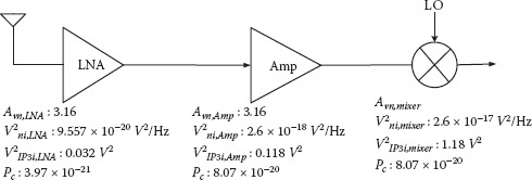
FIGURE 4.9 Optimum-power three-stage receiver with different power coefficients.
Apparently, some corners yield better performance than the others. However, on the corners that give the worst performance, the nonoptimum design has the poorest performance level. It can be seen in Figure 4.8 that the nonoptimum design shows at least 2 dB more degradation of NPD at some corners than the reduced second-order sensitivity design, which achieves the best corner performance. This means that, to achieve the same corner performance from the nonoptimum and the reduced second-order design, one has to improve the NPD of the nonoptimum design by 2 dB. This means that V2ni,tot must be improved by at least a factor of 1.58 and 1/V2IP3i,tot by at least a factor of 1.26, which in turn increases the power consumption by at least a factor of 2 (100%).
As mentioned before, the reduced second-order sensitivity approach is more focused on reducing the sensitivity of the NPD to the gains, whereas the constant-sensitivity approach puts constraints on the sensitivity of the NPD to the noise and nonlinearity. Comparing these two approaches in Figure 4.6, Figure 4.7, and Figure 4.8 reveals that the sensitivity of the NPD to gain variations of individual stages is more influential on the corner and statistical performance than the sensitivity of the NPD to the noise and nonlinearity of individual stages. This is because, for a constant total noise and nonlinearity, reducing the sensitivity of the NPD to the noise or nonlinearity of one stage increases the sensitivity to the noise or nonlinearity of other stages, whereas the sensitivity to the gain of all the stages can be reduced simultaneously.
The reason that the optimum-power design is showing a better corner performance in the preceding example than the constant-sensitivity design is that the NPD has a lower second-order sensitivity to the gain, which in turn is caused by the low power coefficient of the last stage (mixer). However, if the power coefficients are modified as in Figure 4.9, the optimum-power design will be more sensitive to block-level gains. The NPD histograms for both the optimum-power design of Figure 4.4 and that of Figure 4.9 are shown in Figure 4.10. The percentage of samples with NPDs more than 0.5 dB higher than nominal has increased from 8.3% to 18.57%.
Therefore, simultaneous optimum robustness and optimum power can be achieved only if the power coefficients of the rear stages are small compared to those of the front stages.
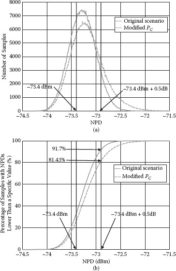
FIGURE 4.10 (a) Number of random samples versus NPD for two optimum-power designs; (b) percentage of random samples with smaller than a specific NPD.
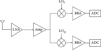
FIGURE 4.11 60 GHz zero-IF receiver including ADC.
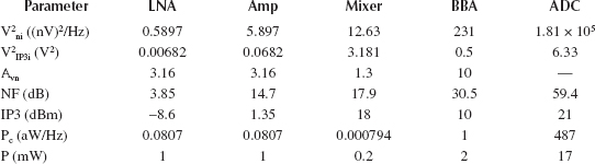
Now we investigate the possibility of applying the design approaches described in Section 4.5 to a 60 GHz receiver including ADC (shown in Figure 4.11). Considering the performance of state-of-the-art components in the 60 GHz band, the system requirements of a receiver including an ADC must be much more relaxed than a system without an ADC. Due to the inefficiency of traditional ADC/DSP approaches at gigahertz bandwidths, many designers tend to eliminate the ADC from the system and replace it with an analog demodulator or a mixed-signal circuit [9,10]. In this system-level study, a state-of-the-art ADC reported in reference 11 is used. The ADC has a sampling rate of 2.5 GS/s, ENOB of 5.4 bits, VDD of 1.1 V, SFDR of –43 dBc, and power consumption of 50 mW. Translating these parameters into the RF domain [12] results in a V2ni of 4.53 × 10⁻¹⁴ V2/Hz and V2IP3i of 5. The parameters of the other components are listed in Table 4.5. These parameters are realistic and consistent with state-of-the-art 60 GHz receiver components [7,8,11].
Using these components, a total noise figure of 12.9 dB and a total IIP3 of –22.8 dBm can be achieved from the receiver. The total power consumption of the receiver will be 155 mW. Assuming an SNDR of 12 dB and a PIMD3i 3 dB below the noise level, the minimum detectable signal for this receiver would be –54.4 dBm. Assuming an output power of 10 dBm for the desired transmitter and an antenna gain of 10 dBi for the transmitter and receiver, this MDS associates with a transmission distance of 6.6 m. Considering the total IP3 of the receiver, the maximum tolerable interferer power at the input of the receiver is –38.9 dBm. Assuming an interfering transmitter with an output power of 10 dBm and residing in a 60° direction, making the gain obtained from antenna 7 dBm, the tolerable interference distance will be 56 cm.
Doing an optimum-power design according to Table 4.6 requires very high performance components, which have not been reported in the literature yet. For example, the required noise figure of the LNA is 2.3 dB, which is well below the best reported figures in the literature [7]. This is due to the fact that the power coefficient of the ADC is much higher than that of the LNA, which results in relaxed specifications for the ADC and demanding specifications for the LNA by the optimum-power approach. However, the resulting specifications for the LNA are not realistic. Therefore, even with such a relaxed overall requirement, optimum-power design is not yet feasible with state-of-the-art CMOS building blocks. Nevertheless, the total power consumption of a receiver designed based on Table 4.6 would be 106.6 mW, which is 31% lower than the receiver in Table 4.5.
TABLE 4.5
Component Parameters for a Nonoptimum Design Including ADC of Reference 11
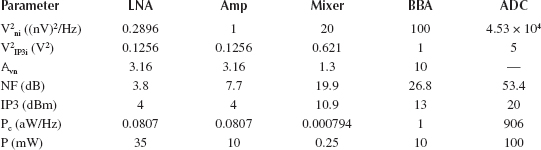
TABLE 4.6
Component Parameters for an Optimum-Power Design Including ADC of Reference 11
This unrealistic prediction by the optimum-power method is due to some assumptions made in the course of development of the method that are not always valid. The assumptions are that the noise and nonlinearity performance of an RF circuit can be improved linearly and indefinitely by just increasing the power consumption and that, for constant power consumption, the noise and linearity performance can be traded for each other, resulting in the prediction of an LNA with 4 mW power consumption and 2.3 dB noise figure. Since these figures are not realistic, we can conclude that these assumptions are not valid in this case or that the case is beyond the validity region of the assumptions.
The optimum power design shown in Table 4.6 has zero first-order sensitivity to the block-level gains, provided that the specified worst-case interferer is –38.9 dBm, satisfying the requirement of (4.36). Designing for low second-order sensitivity to block-level gain variations requires the rear stages of the receiver to have lower contribution to the total noise and nonlinearity distortion. However, since in this case the power coefficient of the ADC is much higher than that of the other components, demanding better noise and linearity performance from the ADC dramatically increases the total power consumption of the receiver.
Although it does not meet the required sampling rate, another ADC reported in the literature has a much better power consumption [13]. With 6.7 mW power consumption, 1 GS/s sampling rate, ENOB of 5, and SNDR of 31.5 dB, this ADC can be considered for a 60 GHz receiver with only half the nominal IF bandwidth (500 MHz). The specifications converted to RF domain are shown in Table 4.7. Using the ADC with the same RF components of Table 4.5 results in a receiver with a power consumption of 68.7 mW, which is less than half of the power consumption of the receiver of Table 4.5. The resulting total NF and IP3 are 18 and –22 dBm, respectively. Although the power consumption is much better, the noise performance is inferior to that of the receiver of Table 4.5. This is not surprising because, although the power consumption of the ADC of reference 13 is 7.5 times smaller than that of reference 20, its power coefficient is only 0.54 of that of reference 11. An optimumpower design with the ADC of reference 13 results in the specifications given by Table 4.8, which are feasible as compared to the specifications of Table 4.6. Please note that the overall performance parameters are still 18 dB of NF and –22 dBm of IP3, which are relaxing compared to those of Table 4.6.
TABLE 4.7
Component Parameters for a Nonoptimum Design Including ADC of Reference 13
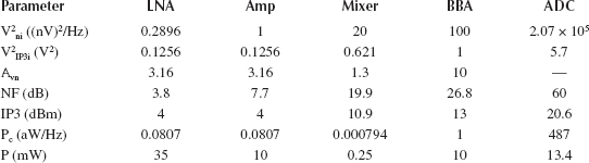
TABLE 4.8
Component Parameters for an Optimum-Power Design Including ADC of Reference 13
The field of ADC design for high speed communication is experiencing rapid progress and new high performance ADCs are reported in the literature that may soon make the ADC/DSP approach possible for millimeter-wave communication links [14].
4.7 ADJUSTMENT OF PROCESS VARIATION IMPACT
According to the presented system-level analysis, the overall performance of a receiver is more sensitive to the noise and nonlinearity of building blocks, which contribute more to the total noise and nonlinearity. Therefore, accumulating the noise and nonlinearity contributions in one stage has the advantage of accumulating the sensitivities in that stage (i.e., the overall performance of the receiver becomes more sensitive to the noise and nonlinearity of that single stage and less sensitive to the noise and nonlinearity of the other stages). This way, the performance degradations resulting from process variations can be compensated mostly by tuning the performance of that single stage. The ideal location for such a stage is at the input of the receiver (i.e., the LNA), resulting in lowered second-order sensitivity to the gains of the stages. In addition, an LNA with tuneable parameters can provide the possibility of input impedance corrections. However, implementing a tuneable LNA is not a trivial task. Furthermore, it is not always easy to accumulate the contributions in the first stage. In the following we compare two strategies of accumulating the contributions in the LNA or in the mixer in terms of feasibility, costs, and benefits.
4.7.1 TUNEABILITY IN DIFFERENT LNA TOPOLOGIES
Figure 4.12 shows three different LNA topologies: a common-gate LNA, an inductively degenerated common-source LNA, and a voltage–voltage transformer-feedback LNA. An inspection of these schematics suggests that the performance of these circuits is determined not only by the operating point and the parasitic of the transistor but also by the value of the inductors. Therefore, in general, one needs to implement tuneable passives, as well as variable biasing for transistors, to deal with the resulting performance degradations. For instance, the input-referred noise voltage of an inductively degenerated common-source LNA is derived from the following:
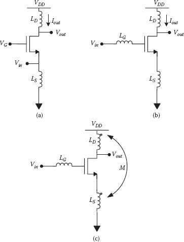
FIGURE 4.12 (a) A common-gate LNA, (b) an inductively degenerated common-source LNA, and (c) a voltage–voltage transformer-feedback LNA.
ˉv2ni = 4KTγgdog2m (R2S + ((LG +LS)ω − 1cgsω)2)(g2mL2Sc2gs + ((LG + LS)ω − 1cgsω)2) c2gsω2((LG + LS)ω − 1cgsω)2 + (gmLScgs + RS)2 |
(4.50) |
According to (4.50), correcting the performance degradations resulting from the variability of cgs and gm (optimistically not including LG and LS) requires using variable biasing and a varactor. Due to the low quality factor of varactors at high frequencies, the noise figure of the LNA would be degraded substantially by using varactors. If the inductors are also prone to variations due to process spreading, variable inductors turn into a necessity. Variable inductors can be implemented using active inductors [15]. However, such circuits fail to behave inductively at millimeter-wave frequencies. In addition, even at low frequencies they tend to deteriorate the noise performance due to the additional active circuitry. Using varactors in parallel with the inductors can also change the effective value of the inductance. However, as mentioned before, this method suffers from the low quality factor of the varactors at high frequencies, which results in unacceptable levels of noise performance.
4.7.2 TUNEABILITY IN OTHER STAGES
If, for some reason, we fail in providing tuneability to the LNA or rendering the LNA the dominant stage in terms of noise and nonlinearity contribution, it is still possible to design other stages, such as mixer, with such properties. In general, as explained before, the overall performance of the receiver is more sensitive to the performance of the stages with highest contribution to the total noise and nonlinearity. Therefore, if the noise and nonlinearity contribution of any stage is dominant compared to that of the other stages, it is practically possible to compensate the effect of process variations by just tuning the performance of that stage. Nevertheless, we know from the system-level analysis that the ideal situation is to accumulate all the contributions in the LNA; only if achieving this ideal becomes infeasible can we opt for accumulation of the contribution, and hence the sensitivities, in other stages.
Furthermore, it is worth noting that achieving the best performance is the first priority for every designer. Therefore, the performance should never be compromised for accumulating the sensitivities in one stage. In other words, any design that provides such property and does not give the required performance is obviously not acceptable.
Choosing the mixer or another IF stage for tuning obviates the need of dealing with delicate, high frequency components. In addition, as we will see later, it is much easier to accumulate the noise and nonlinearity distortion contributions in the mixer.
4.7.3 OVERALL DESIGN CONSIDERATIONS
In the previous subsections, we compared the difficulties of implementing tuneability in the LNA as a high frequency component, and mixer, as a circuit partly located at the low frequency side. In this subsection, we investigate the complexities of accumulating the contributions in the LNA and mixer. A three-stage direct-conversion 60 GHz receiver, shown in Figure 4.13, is considered as a test vehicle for this study.
Two different design strategies are followed and compared. Ideally, as explained in Section 4.5, the ratio between the noise contribution of each stage to that of its following stage must be equal to the ratio between the distortion contribution of the stage to that of its following stage. This, along with an additional condition expressed by (4.35), assures a zero first-order sensitivity of the overall performance to the gains of the individual stages. In the first strategy, represented by receiver 1, the noise and nonlinearity contributions are accumulated in the last stage (mixer). On the other hand, as explained in Section 4.5.2, to reduce the second-order sensitivity of the overall performance to the individual gains, the noise and distortion contribution of the stages must be reduced in a step-wise manner as we move from the front stages to the rear ones. An attempt is made toward reaching this ideal situation in the second strategy. In this strategy, represented by receiver 2, the focus is toward accumulating the noise and nonlinearity contributions in the first stage (LNA).
An inductively degenerated common-source LNA, shown in Figure 4.12(a), and a single-balanced mixer, shown in Figure 4.14, are used in both designs as the first and third stages, respectively. Apart from different component parameters in the first and third stages of receiver 1 and receiver 2, the two receivers use two different circuit topologies as the second stage. A single-stage common-source amplifier is used as the second stage of receiver 1, whereas a two-stage amplifier consisting of an inductively degenerated common-source stage cascaded with a common-source stage is used as the second stage of receiver 2, as shown in Figure 4.15. As a result, the second stage of receiver 2 provides a higher gain.
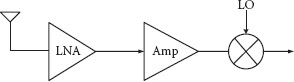
FIGURE 4.13 Three-stage receiver used as the test vehicle in the study.
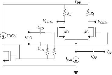
FIGURE 4.14 Single-balanced mixer used in receiver 1 and receiver 2.
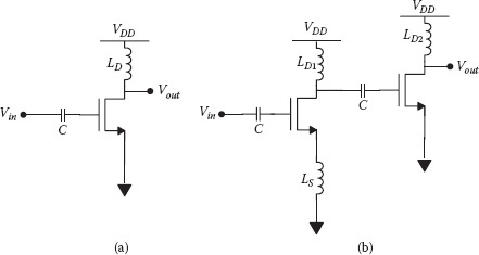
FIGURE 4.15 The second stage in (a) receiver 1, and (b) receiver 2.
Figure 4.16 shows the noise and nonlinearity distortion contribution of each stage in receiver 1. According to Figure 4.16(b), the mixer has the highest contribution to the total nonlinearity distortion. Figure 4.16(a) shows that the mixer and LNA contribute to the total noise almost equally, whereas the noise contribution made by the second stage is smaller. This means that the noise contribution and nonlinearity distortion contribution are mostly accumulated in the mixer. One way to shift this accumulation to the first stage is to design a much more linear and low noise mixer, which is not realistic. Increasing the gain of the second stage can reduce the noise contribution of the mixer. However, it increases the nonlinearity distortion contribution of the mixer.
Figure 4.17 shows the noise and nonlinearity distortion contribution of each stage in receiver 2. The noise contribution of the mixer is well diminished by increasing the gain of the second stage, while its nonlinearity distortion contribution is further increased. Therefore, only receiver 1 has the desired characteristic of accumulating the noise and nonlinearity distortion contribution in one stage. The main reason for not being able to accumulate the contributions in the LNA stems from the very high nonlinearity contribution of the mixer, which cannot be reduced below the nonlinearity contribution of the LNA. However, this is not always true and the possibility of simultaneous accumulation of the noise and nonlinearity contribution in the LNA depends on many factors, such as the utilized circuit topologies, the application, the specifications, and the frequency of operation.
Based on Figure 4.16 and Figure 4.17, neither of the two receivers conforms to the aforementioned required conditions for zero sensitivity to the gains of individual stages. For instance, in receiver 1, the LNA and the mixer have the highest noise contribution, while the LNA shows the lowest distortion contribution. Also, in receiver 2, the LNA has the highest noise contribution and it has the lowest distortion contribution. It appears that the combination of noise and nonlinearity for the blocks, as proposed by the system-level design for zero sensitivity to the gains, is not easily achievable at the circuit level. However, our attempt is to get as close as possible to the ideal situation sketched by the system-level design. Consequently, the desired property of accumulating the noise and nonlinearity distortion contribution in one stage, which is also proposed by the system-level method for facilitating the adaptability, is achieved in receiver 1.
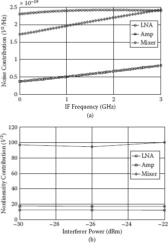
FIGURE 4.16 Contribution of each component in receiver 1 to (a) total noise, and (b) total nonlinearity.
The noise and nonlinearity performances of the two designs are simulated on the process corners and the results are listed in Table 4.9. The power consumption is kept constant on all process corners by keeping the biasing current constant. The simulations are performed with SPECTRE RF periodic steady state, periodic noise, and periodic AC analysis. The VDD is 1.2 V. The LO amplitude is 0 dBm and the LO frequency is 60 GHz. In the next subsection, we investigate the possibility of correcting the performance of receiver 1 on its corners by tuning the performance of the mixer as the stage with accumulated noise and distortion contributions.
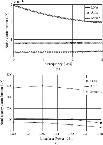
FIGURE 4.17 Contribution of each component in receiver 2 to (a) total noise, and (b) total nonlinearity.
4.7.4 CORRECTING THE CORNER PERFORMANCE
Now that we have a receiver with accumulated noise and nonlinearity distortion contribution in the mixer (receiver 1), the receiver performance degradations resulting from the process variations are expected to be (at least partly) correctable by just tuning the performance of the mixer. This idea is validated by further simulations performed on receiver 1. According to Table 4.9, the highest degradation of the IP3 of receiver 1 occurs at the slow–fast (sf) corner, while the NF is slightly improved at this corner. Choosing IDC3 (used in the biasing of the mixer) as the tuning parameter, the corresponding performance variations are simulated. Figure 4.18 shows the variations of the receiver noise figure as a function of IDC3 at the slow–fast corner. The typical value of IDC3 is 1 mA. According to Figure 4.18, the noise figure has its typical value when IDC3 is 1.87 mA. Then Figure 4.19(b) shows that the IP3 is corrected to above its typical value when IDC3 is 1.87 mA.
TABLE 4.9
Simulation Results of the Two Designs on Process Corners
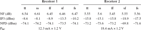
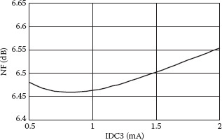
FIGURE 4.18 Noise figure of receiver 1 at sf corner versus IDC3: NF is back to its typical value when IDC3 is 1.87 mA, whereas the typical value of IDC3 is 1 mA.
Figure 4.20 shows the variations of the receiver noise figure as a function of IDC3 at the fast–slow corner. According to Figure 4.20, the noise figure has its typical value when IDC3 is 1.5 mA. Then Figure 4.21(b) shows that the IP3 is corrected to slightly less than its typical value when IDC3 is 1.5 mA.
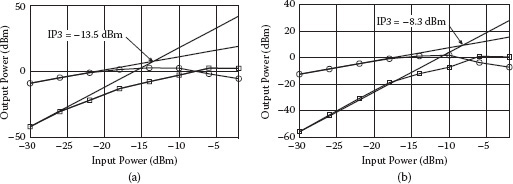
FIGURE 4.19 IP3 of receiver 1 at sf corner for (a) IDC3 of 1 mA, and (b) IDC3 of 1.87 mA.
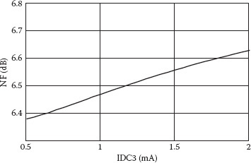
FIGURE 4.20 Noise figure of receiver 1 at fs corner versus IDC3: NF is back to its typical value when IDC3 is 1.5 mA, whereas the typical value of IDC3 is 1 mA.
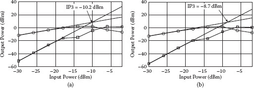
FIGURE 4.21 IP3 of receiver 1 at fs corner for (a) IDC3 of 1 mA, and (b) IDC3 of 1.5 mA.
As a conclusion, these tests validate the possibility of correcting the performance of the whole receiver on the process corners by tuning the performance of only a single stage. This is possible because the noise and distortion contributions are accumulated in that single stage (in this case, the mixer). This possibility can greatly facilitate the correction of process-induced performance degradations in a smart receiver, as it confines the required number of tuneable parameters.
4.7.5 LAYOUT IMPACT APPROXIMATED
To obtain a more accurate estimate of the receiver performance, the impact of the layout is approximated by adding more parasitic resistance and reactance at some specific points. The values of the additional parasitic are calculated based on prior experience with millimeter-wave layout and postlayout simulations. The RF lines, ground lines, and some of the DC lines are modeled by RLC π-networks. The resulting typical performance parameters are shown in Figure 4.22, Figure 4.23, and Figure 4.24.
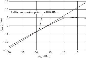
FIGURE 4.22 One-decibel compression point of receiver 1 after approximating the layout impact.
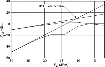
FIGURE 4.23 IP3 of receiver 1 after approximating the layout impact.
Comparing these results with Table 4.9 reveals that the noise performance is hardly degraded after adding the parasitic and the total IP3 is degraded by just 2 dB.
Based on a system-level sensitivity analysis performed on a generic RF receiver, it has been shown that the first-order sensitivities of the overall performance, represented by NPD, to the individual gains of the blocks can all be made zero. Applying the analysis to a zero-IF three-stage 60 GHz receiver shows a significant improvement in the design yield. A quantity called contribution factor is defined as the noise and nonlinearity distortion contribution of each stage with respect to that of its previous stage. Reduction of the second-order sensitivity of the NPD to the gain of individual stages, by keeping the contribution factor of all the stages below one, results in further improvements in the design yield. The conventional optimumpower design methodology has been modified in a way that it nullifies the first-order sensitivities of NPD to the individual gains of all the stages. It has been shown that simultaneous optimum power and optimum robustness can be achieved by using less power-hungry components at the rear stages of the receiver. Applying the analysis to a 60 GHz receiver including ADC shows that state-of-the-art ADCs are not adequate for optimum-power or optimum-robustness receiver design at 60 GHz.
FIGURE 4.24 NF of receiver 1 after approximating the layout impact.
A receiver is designed with good noise and nonlinearity performance and with accumulated noise and nonlinearity distortion contribution in its last stage (mixer). As a result, the overall performance of the receiver is more sensitive to the performance variations of the mixer. Simulations show that it is possible to correct the overall receiver performance degradations resulting from process variations by just tuning the performance of the mixer. In fact, these simulation tests validate the possibility of correcting the performance of the whole receiver on the process corners by tuning the performance of only a single stage (in this case, the mixer and only one parameter of the mixer). This possibility can greatly facilitate the correction of process-induced performance degradations in a smart receiver, as it confines the required number of tuneable parameters. It can also facilitate the performance trimming of the fabricated chips in the production line. The circuits are also simulated with additional parasitics calculated based on previous design experience to approximate the impact of interconnects added during the layout.
1. L.-T. Pang, K. Qian, C. J. Spanos, and B. Nikolic, Measurement and analysis of variability in 45 nm strained-Si CMOS technology. IEEE Journal of Solid State Circuits, vol. 44, no. 8, pp. 2233–2243, Aug. 2009.
2. M. D. Meehan and J. Purviance, Yield and reliability in microwave circuit and system design. Boston: Artech House, 1993.
3. W. Sheng, A. Emira, and E. Sanchez-Sinencio, CMOS RF receiver system design: A systematic approach. IEEE Transactions on Circuits and Systems-I: Regular Papers, vol. 53, no. 5, pp. 1023–1034, May 2006.
4. P. Baltus, Minimum power design of RF front ends. PhD dissertation, Eindhoven University of Technology, 2004.
5. M. El-Nozahi, E. Sanchez-Sinencio, and K. Entesari, Power-aware multiband–multistandard CMOS receiver system-level budgeting. IEEE Transactions on Circuits and Systems II: Express Briefs, vol. 56, no. 7, pp. 570–574, July 2009.
6. Part 15.3: Wireless medium access control (MAC) and physical layer (PHY) specifications for high rate wireless personal area networks (WPANs): Amendment 2: Millimeter-wave based alternative physical layer extension. IEEE 802.15.3c, Oct. 2009.
7. E. Janssen, R. Mahmoudi, E. van der Heijden, P. Sakian, A. de Graauw, R. Pijper, and A. van Roermund, Fully balanced 60 GHz LNA with 37% bandwidth, 3.8 dB NF, 10 dB gain and constant group delay over 6 GHz bandwidth. 10th Topical Meeting on Silicon Monolithic Integrated Circuits in RF Systems, Jan. 2010.
8. P. Sakian, R. Mahmoudi, E. van der Heijden, A. de Graauw, and A. van Roermund, Wideband cancellation of second order intermodulation distortions in a 60 GHz zero-IF mixer. 11th Topical Meeting on Silicon Monolithic Integrated Circuits in RF Systems, Jan. 2011.
9. A. Tomkins, R. A. Aroca, T. Yamamoto, S. T. Nicolson, Y. Doi, and S. P. Voinigescu, A zero-IF 60 GHz 65 nm CMOS transceiver with direct BPSK modulation demonstrating up to 6 Gb/s data rate over a 2 m wireless link. IEEE Journal of Solid State Circuits, vol. 44, no. 8, pp. 2085–2099, Aug. 2009.
10. C. Marcu, D. Chowdhury, C. Thakkar, J.-D. Park, L.-K. Kong, M. Tabesh, Y. Wang, et al., A 90 nm CMOS low-power 60 GHz transceiver with integrated baseband circuitry. IEEE Journal of Solid State Circuits, vol. 44, no. 12, pp. 3434–3447, Dec. 2009.
11. E. Alpman, H. Lakdawala, L. R. Carley, and K. Soumyanath, A 1.1V 50 mW 2.5 GS/s 7 b time-interleaved C-2C SAR ADC in 45 nm LP digital CMOS. IEEE International Solid State Circuits Conference, Feb. 2009.
12. W. Deng, R. Mahmoudi, P. Harpe, and A. van Roermund, An alternative design flow for receiver optimization through a trade-off between RF and ADC. IEEE Radio Wireless Symposium, Jan. 2008.
13. J. Yang, T. Lin Naing, and R. W. Brodersen, A 1 GS/s 6 bit 6.7 mW successive approximation ADC using asynchronous processing. IEEE Journal of Solid State Circuits, vol. 45, no. 8, pp. 1469–1478, Aug. 2010.
14. B. Verbruggen, J. Craninckx, M. Kuijk, P. Wambacq, and G. Van der Plas, A 2.6 mW 6 b 2.2 GS/s 4-times interleaved fully dynamic pipelined ADC in 40 nm digital CMOS. IEEE International Solid-State Circuits Conference Digest of Technical Papers, pp. 296–298, Feb. 2010.
15. C.-L. Ler, A. K. bin A’ain, and A. V. Kordesch, Compact, high-Q, and low-current dissipation CMOS differential active inductor. IEEE Microwave and Wireless Components Letters, vol. 18, no. 10, pp. 683–685, Oct. 2008.