
Ultralow Power Radio Design for Emerging Healthcare Applications |
|
CONTENTS
10.1.1 WBAN and Healthcare Applications
The rapid growth in physiological sensors, low power integrated circuits, and wireless communication has enabled a new generation of wireless sensor networks for healthcare. The wireless body area network (WBAN) is a new wireless network that could allow inexpensive continuous health monitoring and early detection of medical patient conditions via the Internet. Intelligent physiological sensors can be placed on, in, or around the human body to collect various physiological changes in order to monitor the patient’s health status no matter where the patient is [1,2]. The information will be transmitted wirelessly to an external base station, mostly in the form of a smart phone. The base station will instantly transmit all information in real time to the healthcare providers. If an emergency is detected, the patient and his or her caregivers will be immediately informed to take the required actions. The development of telehealth solutions is pushed by large industry alliances such as Continua [3]. And in the last few years, telemonitoring products have been introduced in the area of cardiac health management by companies like Cardionet [4], Corventis [5], AliveCor [6], and Airstrip [7]. In parallel, several pilot trials have been reported for the use of WBAN technologies in various applications (e.g., for sleep [8] or epilepsy monitoring [9]). The WBAN concept allows patients to stay in their home environment and hence have a better quality of life with lower costs involved. The reduced cost of this concept is a necessity as the cost of healthcare in First World countries is increasing dramatically as a result of advances in medicine, a population that is becoming older, and an increasingly unhealthy lifestyle.
The benefits from these technological advances highlight the need for rapid development of WBAN technology. This chapter presents a research overview in the field of wireless body area networks. More specifically, in the chapter an ultralow power radio design for these emerging healthcare applications is presented. To provide proper context of the research we will start by discussing some prototypes of current health monitoring systems and discuss the requirements of wireless systems for future WBAN healthcare applications. Second, we will present link budget analysis that is carried out in order to determine the expected performance of such systems. Third, we will discuss the design and the implementation of the ultralow power BAN radio. Also, we will show the evaluation of the BAN radio system level performances in the BAN environment. The chapter will end with a summary and conclusions.
10.1.1 WBAN AND HEALTHCARE APPLICATIONS
The technology breakthroughs in WBAN can lead to new application opportunities in the areas of health, wellness, and lifestyle. Examples of applications include
• Vital signals monitoring (EEG, ECG, EMG, temperature, respiratory, heart rate, pulse oximeter, blood pressure, oxygen, pH value, glucose, cardiac arrhythmia)
• Wireless capsule endoscopes (gastrointestinal)
• Wireless capsules for drug delivery
• Deep brain stimulators
• Cortical stimulators (visual neurostimulators, audio neurostimulators, Parkinson’s disease)
• Remote control of medical devices (pacemaker, actuators, insulin pumps)
• Hearing aids
• Retina implants
• Disability assistance (muscle tension sensing and stimulation, wearable weighing scale, fall detection, aiding sport training).
In this section, we will focus on three prototypes of the current health monitoring systems and discuss the requirements of wireless systems for future WBAN health-care applications.
The first prototype is a wireless electrocardiography (ECG) system for cardiovascular disease monitoring. Cardiovascular disease is the number one cause of death and disability in the United States and most European countries. Heart diseases, among which are cardiac arrhythmias, are estimated to account for 30% of all death in the United States. Nowadays, diagnosis of cardiac arrhythmias is performed by point-of-care ECG monitoring or using Holter devices. Very recently, a new wave of portable patient monitors has been introduced, targeting outpatient monitoring with embedded detection of arrhythmia [4]. It is recognized that treatment and prevention of many cardiovascular diseases would benefit from a wireless ECG system for long-term continuous monitoring, but technology barriers have so far prevented the widespread use and acceptance of such a continuous ECG monitor on a daily basis. Such a device should be a very small wireless device, with no required battery replacement, that analyzes the data online and takes appropriate actions in case of emergency. The device should not affect the wearer in his daily life activity while constantly looking over his health.
A wireless ECG patch prototype [10] is illustrated in Figure 10.1. This prototype combines technologies for ultralow power biopotential readout, optimized power management, and advanced electronic integration on flexible substrate. Depending on the application, the ECG patch streams the one-channel ECG data to a receiver within a 10 m range, or performs local analysis on the data to extract R-peak and other fiducial points. Power consumption of the system has been reported to be 1.17 mW in data streaming mode, and 1.74 mW if the data are processed locally and sent at every beat [10]. The latter value is due to a heavy usage of the microcontroller resources, pointing to an important limitation of today’s off-the-shelf microcontrollers. Targeted at very low processing duty cycles, they become quickly limiting for applications requiring quite advanced embedded digital signal processing (DSP) capabilities. This reinforces the need for ultralow power DSP technology in the future.
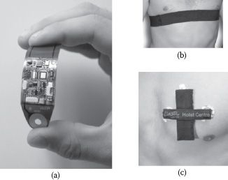
FIGURE 10.1 (a) Wireless ECG patch integrated on flexible substrate; (b) chest belt package; (c) textile pocket package.
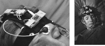
FIGURE 10.2 Prototype wireless body area network for sleep staging.
The second prototype is a wireless device for sleep monitoring. Sleep disorders are known to affect a significant part of the population: up to 10% of the American population and 4% of the European population. Typical diagnosis of sleep disorders is performed using polysomnography tests at the point of care. Ambulatory sleep monitoring devices have been introduced for home monitoring and prescreening. However, they suffer from important burdens such as their weight (mainly due to the battery) and the high density of wires going from the head to the data acquisition box (often located around the belt). Centers for sleep disorders would benefit from a miniaturized, wire-free, sleep-staging system, targeting the monitoring of the patient’s hypnogram—that is the sequence of sleep stages overnight. The development of a prototype WBAN for wireless sleep staging was reported in Romero Legarreta et al. [11]. It relies on the ultralow power single-channel biopotential readout chip described in Yazicioglu et al. [12]. Its low power consumption (60 μW) allows dramatic reduction of the size of the battery, hence of the entire system, while maintaining an autonomy suitable for sleep analysis (>12 hours).
The system, illustrated in Figure 10.2, consists of a body sensor network composed of three wireless sensor nodes, collecting data from two-channel electroencephalography (EEG), two-channel electro-oculography (EOG), and one-channel electromyography (EMG), and sending it wirelessly to a receiver located in the patient’s room. These particular signals were selected according to the Rechtschaffen and Kales standards for sleep staging [13]. The data can then be analyzed, on- or off-line, by the clinical staff. Each node achieves a power consumption of 15 mW, for a sampling rate of 200 Hz. Thanks to their small size and light weight, the three sensor nodes can easily be integrated in a headband, hence increasing patient comfort and acceptance.
The third prototype is the system for emotion monitoring. Monitoring the emotional state of human beings is becoming increasingly popular, with applications in psychophysiology (e.g., stress management), gaming, and human–computer interaction. The autonomic nervous system (ANS) is part of the body control system responsible for maintaining stability in the body. It affects the regulation of body parameters such as heart rate, respiration rate, salivation, and perspiration in response to external conditions and events. This unconscious process reveals valuable information to interpret the emotional state of a human being, such as arousal. The concept of WBAN is applicable to monitoring physiological changes in the autonomic nervous system that carry much of the information related to arousal responses to external or internal stimuli. Brown et al. [14] developed a customized emotion monitoring system by monitoring four physiological signals: ECG, respiration, skin conductance, and skin temperature. Each of these modalities is known to be regulated by the autonomic nervous system and thus represents interesting candidates to capture emotional responses to external stimuli [14,15].
The system, illustrated in Figure 10.3, consists of two low power miniaturized body sensor nodes that communicate with a receiver connected to a PC or to a data logger. The first node is integrated in a wireless chest belt and monitors ECG (lead-I) and respiration. The second node is integrated in a wireless wrist sensor and monitors skin conductance and skin temperature. Each node is composed of a generic wireless node, to which are connected the corresponding sensor front-end boards.
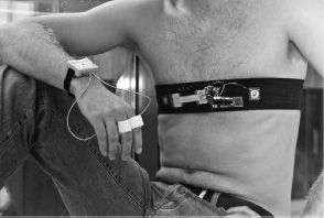
FIGURE 10.3 Integrated body area network for ambulatory monitoring of physiological responses from the autonomic nervous system.
From this, it is clear that WBAN is an interdisciplinary area that could allow inexpensive and continuous health monitoring with real-time updates of medical records. The number of applications where WBAN can be applied is very large. Therefore, a universal WBAN system should allow scalable data rates ranging from 10s of kbps to 1 Mbps such that most of the WBAN applications could be supported. Furthermore, the prototypes presented earlier can only operate from a few days to a week at full functionality. This is not enough, especially for implantable communications where months or years of autonomy are expected. Early demonstrators of autonomous wireless health monitors have shown that harvesting energy from the environment during the operation of the system will allow the system to run eternally with a battery or a supercapacitor acting only as a temporary energy buffer. But as the overall size and weight of sensor nodes are also an important design issue, it is impossible for the energy harvester to generate infinitely large energy. For example, a 1 cm2 area of the current energy harvesters can only generate power in the range of 10 μW to 1 mW [2]. Thus, the ultralow power wireless system consuming less than 1 mW is expected to enable autonomy and miniaturization of WBAN.
Successful design of wireless systems for healthcare applications involves many factors. However, a top-level link budget analysis is the first step to be carried out in order to determine the expected performance of such systems in a given channel scenario. It is also an excellent means to the understanding of various factors that must be traded off in terms of complexity and performance.
At higher data rates of up to 1 Mbps, the state-of-the-art super-regenerative front ends can achieve sensitivity from –60 dBm [16,17] up to –70 dBm [18], while keeping the power consumption sufficiently low. Taking this into account in the link budget analysis, the target specification of the transceiver for health applications can be finalized. Normally the receiver sensitivity could be computed as follows:
(10.1) |
where Pt, PL, Gt, and Gr represent the transmit power, path loss, transmit antenna gain, and receiver antenna gain, respectively. From (10.1) it is clear that the path loss is a very important factor determining the receiver power. Please note that path loss is rapidly changed in close spatial proximity to a particular location caused by the multipath. This variability is called the small-scale fading and is often characterized by a channel model. Thus, to take the variation of the path loss into account for link budget calculation, we should choose practical channel models.
The channel model considered here is the one for the body surface to external communication at 2.4 GHz proposed from the IEEE 802.15.6 working group [19]. This channel model assumes that the transmitter is placed on the chest and the receiver is away from the body with various distances. It considers both the standing and walking scenarios. Thus, the effects of the body movement on system performance could also be investigated. Note that different distributions (e.g., gamma distribution, lognormal distribution) are used to characterize the small-scale fading for different scenarios.
For determining the target receiver sensitivity and transmit power, we define that the system is reliable if the channel path loss is sufficiently small such that the received signal strength exceeds the receiver sensitivity [20]. The probability of this reliability is dependent on the channel small-scale fading. To decouple the antenna effect, we assume that the antenna gain of 0 dBi is here. From Table 10.1 we find that 0 dBm transmit power and –75 dBm receiver sensitivity are sufficient since the probability of reliability is always larger than 95%, which is a typical requirement in WBAN [21].
However, when the receiver sensitivity is –65 dBm, the system is not always reliable, especially in the walking scenario at 4 m transmission distance, as shown in Table 10.2. Therefore, we choose the 0 dBm transmit power with a receiver sensitivity of –75 dBm as our target specification in wireless system design for WBAN.
TABLE 10.1
Probability of Reliability When Transmit Power is 0 dBm and Receiver Sensitivity Distance is −75 dBm
Distance (m) |
1 |
2 |
3 |
4 |
Standing |
~100% |
~100% |
~100% |
~100% |
Walking |
99.72% |
99.61% |
~100% |
99.99% |
TABLE 10.2
Probability of Reliability when Transmit Power is 0 dBm and Receiver Sensitivity is −65 dBm
Distance (m) |
1 |
2 |
3 |
4 |
Standing |
~100% |
~100% |
~100% |
93.97% |
Walking |
98.13% |
95.87% |
98.39% |
79.57% |
It is known that the radio often consumes between 50% and 85% of total sensor power consumption for the kind of BAN applications mentioned earlier [2,22]. As an example, an ECG necklace has been integrated (see Figure 10.4a). This two-lead ECG necklace transmits an ECG signal without any motion artifact compensation or other algorithms done on the necklace. The ECG necklace was created using off-the-shelf but best-in-class minimal power consumption components. The sensor readout was specifically developed [12] because it was impossible to find sensor readout with sufficient specifications and low enough power consumption. When optimally using all available power modes, the average power consumption of 0.903 mW* is achieved. In Table 10.3 the ECG application parameters are summarized. Table 10.4 shows the list of the components used in the ECG necklace, while Figure 10.4(b) shows the breakdown chart for the power consumption. Please note that the radio transmission rate for this example is extremely low and that, for higher radio transmission rates, the power consumption of the radio further increases.
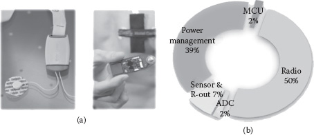
FIGURE 10.4 Sensor node: (a) wireless ECG necklace; (b) power budget with average power optimally using all available modes and duty cycling.
TABLE 10.3
ECG Application Parameters
Application parameter at the electronics level |
Value |
Listening interval (ms) |
100 |
Reception time slot (ms) |
2 |
Transmission interval (ms) |
35 |
Number of bits per sample (transmission) (bit) |
12 |
Sampling interval (ms) |
2.5 |
Transmission/reception range (m) |
10 |
TABLE 10.4
Components Used in ECG Necklace Made with Off-the-Shelf Components and Imec Biopotential
Component |
μC: MSP430 |
Radio: Nordic nRF24L01 |
ADC: MSP430 |
Power manager: TP780 |
Biopotential: Imec |
The analysis of the sensor power budget shows that the radio is the most power hungry block. Therefore, a new radio can reduce the overall power consumption of the system significantly. The design of an ultralow power radio is a challenging task. To reduce power as much as possible, a low complexity, nonlinear architecture seems a good choice. A combination of on/off keying (OOK) modulation, a direct modulation transmitter, and super-regenerative receiver principle [23] enables ultralow power consumption, thus providing a suitable architecture for autonomous body area network (BAN) sensor nodes.
10.1.3.1 System Architecture
A block diagram of the BAN transceiver that we have implemented is shown in Figure 10.5 [24,25]. Next to the direct modulation transmitter (Tx) and super-regenerative receiver (Rx) front end, this work integrates analog and digital baseband and PLL functionality. The transceiver supports additional programmability for flexible data rates and achieves ultralow power consumption for the overall system. For lower power consumption and better performance, the Tx and Rx matching networks are placed externally. The serial peripheral interface (SPI) host interface links our designed chip with the MSP 430 microprocessor for data and control information communication.
10.1.3.2 Transmitter Front End
A block diagram of the implemented direct modulated Tx is presented in Figure 10.6 [26]. The direct modulation transmitter architecture simplifies the stage preceding the power amplifier (PA). This reduces the power overhead from the pre-PA stages [27] and increases the Tx power efficiency. In the Tx, the 2.4 GHz carrier is generated by the integrated LC voltage-controlled oscillator (VCO), and amplitude modulation is applied on the PA. Between the PA and the VCO, a low power buffer is inserted to avoid the dynamic loading effect from the PA. This improves the frequency stability of the VCO. To avoid spectrum artifacts during the VCO start-up period, only the PA is switched on and off in our architecture. This also increases the data rate since the start-up time of an LC VCO with reasonable Q-factor is much longer than the time needed to switch the PA on or off. To ensure optimal power efficiency despite PVT variations, we have designed a duty cycled swing detector that will monitor and adjust the driving level of the PA. The complete transmitter also implements digital pulse shaping for improved spectral efficiency. The digital baseband oversamples the baseband bit stream by 6× and shapes the OOK pulse with a predetermined filter (e.g., the raised cosine (finite impulse response) FIR filter).
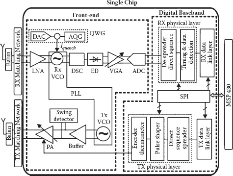
FIGURE 10.5 Block diagram of the implemented ULP OOK transceiver.
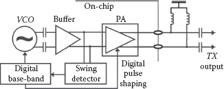
FIGURE 10.6 Block diagram of the implemented direct modulated transmitter.
The Tx front end is optimized to transmit 0 dBm output power as it is required by the link budget analysis. It consumes 2.53 mW at 1 V supply voltage for 50% OOK. The overall efficiency of the Tx front end is 24% when transmitting continuous ones, while the efficiency for both zeros and ones reaches 40%. More details regarding the Tx front-end implementation and the achieved results are presented in references 24–26.
10.1.3.3 Receiver Front End
Due to its simplicity and low power expenditure, super-regeneration is a commonly employed principle in the Rx of sensor networks [16,17,28]. A block diagram of the implemented ULP super-regenerative Rx front end is shown in Figure 10.7 [24,25]. The LNA provides input matching for the antenna, amplifies the RF signal, and improves the isolation between the antenna and the VCO. The VCO is the main part of the super-regenerative receiver. It is biased with a time-varying quench current Iquench [23] from the quench waveform generator (QWG). In the presence of an input signal, the VCO oscillations build up faster. The signal detection can be based on a difference in the VCO start-up time for the logarithmic mode or on a difference in the VCO amplitude for the linear mode [25].
In our implementation, the Rx is optimized for the linear mode. The linear mode will provide a higher data rate because the VCO does not need additional time to reach saturation, and the VCO discharging is shorter. Further, the quench current Iquench is generated in a combined analog and digital fashion to achieve both low power consumption and higher data rate [29]. The differential-to-single-ended converter (DSC) in the Rx provides the differential to single-ended conversion of the signal and suppresses the common-mode level from the VCO. The envelope detector (ED) performs the down-conversion of the wanted signal to DC. The variable gain amplifier (VGA) adjusts the signal to fit into the dynamic range of the analog-to-digital converter (ADC). The VGA is partially open loop to reduce the power consumption [25]. The 8-bit successive approximation (SAR) ADC [30] uses asynchronous dynamic logic and custom-built 0.5 fF capacitors to achieve low power at high speed.
The Rx front end operates up to 5 Mbps, for which it achieves –75 dBm sensitivity for bit error rate (BER) of 10–3 while it consumes 534 μW. At 0.5 Mbps it achieves –78 dBm sensitivity. More details regarding the Rx front-end implementations and achieved results are summarized in references 24, 25, and 29.
10.1.3.4 PLL
The phase-locked loop (PLL) sets the desired channel in the radio. In the proposed transceiver architecture, the VCO is part of the signal path in both the Tx and Rx. Because the Tx and the Rx have different constraints for the VCO, they use a separate VCO, while sharing the same PLL. Figure 10.8 shows the architecture of the integer-N PLL implemented in this prototype [24,25]. The phase/frequency detector (PFD), the charge pump (CP), the loop filter (LPF), and the divider-by-M are shared between the Tx and the Rx, while each VCO has its own buffer and a 30/32 prescaler. Each 30/32 prescaler consists of a divider-by-2 and a divider-by-15/16. With multiplexers MUX1 and MUX2, the PLL can be activated for either the Tx or the Rx. Also, external analog tuning can be applied instead of using the PLL. With a 500 kHz reference frequency (fref), the PLL locks the VCO frequency from 2.36 to 2.485 GHz with increments of 15 or 16 MHz, dependent on the setting of the divider-by-15/16. The PLL consumes 1.1 mW from a 1.2 V supply.
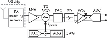
FIGURE 10.7 Block diagram of the implemented super-regenerative receiver front end.
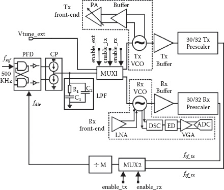
FIGURE 10.8 Block diagram of the implemented integer-N PLL.
Because of the quenched operation in the super-regenerative receiver, the VCO is continuously enabled and disabled. For this reason a continuous feedback PLL is not possible. Therefore, during the Rx frequency locking mode, the Rx VCO is biased with a constant current as shown in Figure 10.9. During this time, the PLL is enabled to lock the VCO to the desired frequency. After that, the PLL is disabled, and the Rx starts the receiving mode (tRX). In the transmission mode, the PLL can also be disabled to decrease power consumption further. The system-level measurements show that the Rx is able to receive packets with packet error rate (PER) of 10–2 in 25 ms time at 1 m line of site (LOS) distance while the PLL is off. Within 25 ms, the Rx is able to receive five packets with a maximum packet size of 5 ms.
10.1.3.5 Receiver Timing
On the Rx side, the receiver timing is important and it is controlled by three clocks from the digital baseband: an_clk_qch, dig_clk_qch, and ADC_clk. The Rx timing is shown in Figure 10.10.
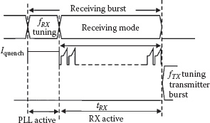
FIGURE 10.9 Rx/PLL timing.
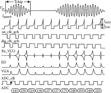
FIGURE 10.10 Receiver timing.
In order to achieve better performance, in our implementation a received signal VIN is 3× oversampled by the quench signal. In this way better peak synchronization will be achieved. By omitting oversampling, the data rate can be increased to the quench rate, but additional synchronization is needed. Further, the shape of Iquench is controlled by dig_clk_qch and an_clk_qch. In this way the VCO on-time is controlled. The ADC samples the output of the VGA on the rising edge of the ADC_clk. Each of the control clocks is derived from a 6 MHz baseband clock by a dedicated clock generator. In order to maximize the performances, the phase and duty cycle of each clock is programmable with a resolution of 750 ps [24,25].
10.1.3.6 Digital Baseband
The digital baseband operates at 6 MHz clock and is supplied by a single 1.2 V power supply. Apart from the clock generation, the digital baseband includes the transmitter data link layer, the transmitter physical layer, the receiver physical layer, the receiver data link layer, and the SPI host interface, as shown in Figure 10.11. In the physical layer, to achieve the scalability of data rate and robustness, the direct-sequence spread spectrum (DSSS) technology [31] is used. This technology spreads the baseband signal coming from the data link layer by directly multiplying the bit with a pseudonoise (PN) sequence consisting of a number of PN code symbols. The PN code symbol is called the chip and the number of chips in 1 bit can be 1, 2, 4, or 16 in implementation. In the data link layer, the CCITT CRC-16 code [32] is used to check whether there are data errors in packet transmission. The SPI host interface links our designed chip with the external host processor such as the microprocessor or the field-programmable gate array (FPGA) for data and control information communication.
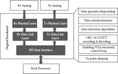
FIGURE 10.11 Digital baseband.
In the transmitter side, the raw data bits from the SPI host interface are assembled in the transmitter data link layer as packets, at the end of which 16 cyclic redundancy check (CRC) bits are generated based on the CCITT CRC-16 code and the raw data bits within the packet. In the transmitter physical layer, the bit is spread over chips. Each chip is further passed through a pulse shaper to make the transmitted signal better suited to the communication channel. The shaped digital signal is passed through the thermometer encoder, which translates the signed 6-bit values into unsigned 15-bit values for the PA in the transmitter analog front end.
In the receiver side, the output data from the ADC is first passed to the receiver physical layer, where the data dispreading, time synchronization, and data detection algorithms are performed. In addition, a VGA updating algorithm, used to increase the sensitivity of the data detection (by avoiding clipping of the ADC samples), has been implemented in the physical layer. The detected bits within one packet will then be verified in the data link layer by comparing the detected CRC bits with the one freshly calculated from the detected data bits. Finally, the detected data bits are passed to the external host processor through the SPI host interface for further processing.
10.1.3.7 Radio Measurements in BAN Environment
The BAN radio has been implemented in 90 nm CMOS. The die photo of the radio is shown in Figure 10.12. It occupies 2.4 × 1.85 mm2.
The system-level performance of the BAN radio has been evaluated. From our measurement results, PER of 10–2 is achieved within 25 m line-of-sight (LOS) transmission distance wireless communication. This maximum distance is achieved for 1 Mbps chip rate when PN sequence of 16 is applied. This will result in a total of 62.5 kbps achieved data rate. The packet size is 288 bits.
The measurement results of the BAN radio are achieved for the power consumption summarized in Figure 10.13. The measured Tx power consumption is for 50% OOK 0 dBm transmit power. The Tx front end consumes 4.192 mW when transmitting “1” and 0.868 mW when transmitting “0.” The measured Rx power consumption is for a 1 Mbps input signal oversampled at 3 MHz quench rate. The digital baseband is running at 6 MHz clock. The peak current of the PLL is 915 μA from 1.2 V. Since the duration of the Tx/Rx frequency locking modes is negligible compared to the duration of the transmitting/receiving modes, the contribution of the PLL to the total transceiver power can be neglected.
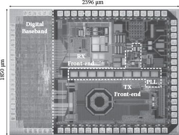
FIGURE 10.12 Die photo of the single-chip transceiver.
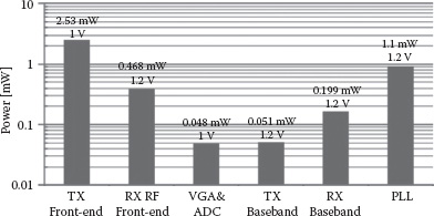
FIGURE 10.13 Power consumption summary.
Further, we have evaluated the system performance of the developed transceiver chip in the BAN environment. The measurement evaluation is based on our prototyped ECG necklace (see Figure 10.4) with the BAN radio and the corresponding base station as shown in Figure 10.14. The base station consists of our integrated BAN transceiver chip to receive the signal, an MSP430 microcontroller to read data from the transceiver chip, and the UART-USB bridge to transfer the data from the microcontroller to the computer through a USB cable. Through the cable, 5 V power is also provided to the power management circuitry of the base station. In this system we first evaluated the power consumption of the ECG necklace as discussed in Section 10.1.3, where the Nordic radio is replaced with our BAN radio. When replacing the original Nordic radio with the ULP BAN radio, the system power consumption is reduced to 0.366 mW and 2.5× power reduction at system level is achieved. The new power breakdown is shown in Figure 10.15.
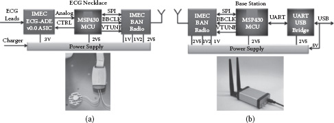
FIGURE 10.14 (a) ECG necklace; (b) base station.
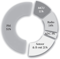
FIGURE 10.15 Power breakdown of optimized ECG necklace with Imec biopotential and Imec BAN radio.
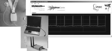
FIGURE 10.16 Heart’s electrical activities measured by using the ECG necklace.
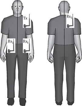
FIGURE 10.17 Antenna positions in BAN measurements.
The ECG necklace together with the base station is used to monitor the heart’s electrical activities for fitness or healthcare applications, as shown in Figure 10.16.
In the measurement, as illustrated in Figure 10.17, we placed the Tx (ECG necklace) close to the heart position (i.e., the left side of the chest) and placed the Rx (the base station) on the left pocket (Rx1), right pocket (Rx2), or the back (Rx3) in order to represent the situation that the sensed ECG signal from the sensor node is sent to a relay node for further processing. We used the PER to evaluate the system performance. The considered PER is the result of the synchronization error (both the missed detection and false alarm) and data detection error:
• Misdetection error: the packet is transmitted while not detected by the synchronization algorithm.
TABLE 10.5
PER for Different BAN Scenarios
Rx |
Rx1 |
Rx2 |
Rx3 |
PER |
<0.1% |
0.4995% |
1.4% |
• False alarm: the start frame delimiter (SFD), which indicates the end of the preamble, is wrongly detected.
• Data detection error: the packet is in error if at least one data bit within the packet is wrongly detected.
To compute the value of each PER, we use 1,000 packets. Thus, when the PER is below 0.001, the results are less reliable and will be shown only as <0.1%. The transmit power is set to 0 dBm.
From Table 10.5, it is clear that the transmission along the front side of the body (i.e., heart to left pocket) results in the best performance, as expected, since the transmission distance is the shortest and it is in the line-of-sight scenario. The transmission from the front to the back of the body (i.e., heart to back) has the worst scenario. However, it can still achieve a PER of around 1%, which is sufficient for many BAN applications.
In this chapter an ultralow power radio for emerging healthcare applications has been presented. To provide proper context of the research, the chapter first highlights the benefits from the WBAN technology. The technology breakthroughs in WBAN can lead to new application opportunities in the areas of health, wellness, and lifestyle. Some examples of applications are vital signals monitoring such as EEG, ECG, EMG, temperature, respiratory, heart rate, pulse oximeter, blood pressure, oxygen, pH value, glucose, and cardiac arrhythmia. Further, the wireless networks can be used in wireless capsule endoscopes (gastrointestinal), wireless capsules for drug delivery, deep brain stimulators, visual neurostimulators, audio neurostimulators, remote control of medical devices (pacemaker, actuators, insulin pump), hearing aids, retina implants, and disability assistance. The benefits of the wireless ECG system for cardiovascular disease monitoring, the wireless device for sleep monitoring, and the system for emotion monitoring have been discussed in more detail.
From the application study it has been clearly shown that the number of applications where WBAN can be applied is very large. This will require a universal WBAN system with scalable data rates ranging from tens of Kbps to 1 Mbps such that most of the WBAN applications could be supported. Furthermore, the ultralow power wireless system consuming less than 1 mW is expected to enable autonomy and miniaturization of WBAN. For that purpose we have designed and implemented an ultralow power radio that can be used in WBAN applications. The radio can operate in 2.36–2.4 GHz medical BAN and 2.4–2.485 GHz ISM band. The Tx of the BAN radio transmits the OOK signal with 0 dBm peak power. Including the Tx baseband, the complete transmitter consumes 4.243 mW when transmitting “1” and 0.919 mW when transmitting “0,” which leads in 2.59 mW with 50% OOK. The Rx front end of the BAN radio achieves –75 dBm sensitivity at 5 Mbps and –78 dBm at 0.5 Mbps. The complete receiver consumes 715 μW at 1 Mbps data rate, over-sampled at 3 MHz. The transceiver achieves PER = 10–2 at 25 m line-of-site with 62.5 kbps data rate and 288-bit packet size, and it has been incorporated in an ECG necklace to monitor the heart’s electrical property. This necklace has a 2.5× power reduction at system level when compared to the original necklace with a best-in-class, off-the-shelf radio.
1. R. Schmidt, T. Norgall, J. Mörsdorf, J. Bernhard, and T. von der Grün, Body area network, BAN, a key infrastructure element for patient-centered medical applications. Biomedical Technology, vol. 47 (s1a), pp. 365–358, Jan. 2002.
2. L. Huang, M. Ashouei, F. Yazicioglu, J. Penders, R. Vullers, G. Dolmans, P. Merken, et al., Ultra-low power sensor design for wireless body area networks: challenges, potential solutions, and applications. International Journal Digital Content Technology and Applications, vol. 3, no. 3, pp. 136–148, Sept. 2009.
3. Continua Health Alliance: www.continuaalliance.org
5. http://www.corventis.com/us/default.asp
7. http://www.airstriptech.com/
8. N. de Vicq, F. Robert, J. Penders, B. Gyselinckx, T. Torfs, Wireless body area network for sleep staging. Proceedings International Conference on Biological Circuits and Systems, 2007.
9. F. Massé, J. Penders, A. Serteyn, M. van Bussel, and J. Arends, Miniaturized wireless ECG-monitor for real-time detection of epileptic seizures. In Wireless health 2010 (WH ‘10). New York: ACM, 111–117, 2010.
10. J. Penders, B. Gyselinckx, et al. Human++: From technology to emerging health monitoring concepts. Proceedings of the 5th International Workshop on Wearable and Implantable Body Sensor Networks, Chinese University of Hong Kong, China, June 1–3, pp. 94–98, 2008.
11. I. Romero Legarreta, P. Addison, N. Grubb, G. Clegg, C. Robertson, K. Fox, and J. Watson, Continuous wavelet transform modulus maxima analysis of the electrocardiogram: Beat characterization and beat-to-beat measurement. International Journal of Wavelets, Multiresolution and Information Processing, vol. 3, no. 1, pp. 19–42, 2005.
12. R. F. Yazicioglu, P. Merken, R. Puers, et al., A 60 μW 60 nV/√Hz readout front end for portable biopotential acquisition systems. IEEE Journal Solid-State Circuits, vol. 42, no. 5, pp. 1100–1110, May 2007.
13. A. Rechtschaffen and A. Kales, A manual of standardized terminology, techniques and scoring system for sleep stages of human subjects. Washington, DC: US Government Printing Office, National Institute of Health Publication, 1968.
14. L. Brown, B. Grundlehner, J. van de Molengraft, J. Penders, and B. Gyselinckx, Body area networks for monitoring autonomous nervous system responses. Proceedings of the International Workshop on Wireless Pervasive Healthcare, London, April 2009.
15. B. Grundlehner, L. Brown, J. Penders, and B. Gyselinckx, The design and analysis of real-time, continuous arousal monitor. Proceedings of the 6th International Workshop on Wearable and Implantable Body Sensor Networks, pp. 156–161, 2009.
16. J. Y. Chen et al., A fully integrated auto-calibrated super-regenerative receiver in 0.13 μm CMOS. IEEE Journal Solid-State Circuits, vol. 42, pp. 1976–1985, 2007.
17. D. Shi, N. Behdad, J. Y. Chen, and M. P. Flynn, A 5 GHz fully integrated super-regenerative receiver with on-chip slot antenna in 0.13 μm CMOS. IEEE Symposium on VLSI Circuits, pp. 34–35, 2008.
18. J. Ayers et al., A 0.4 nJ/b 900 MHz CMOS BFSK super-regenerative receiver. IEEE CICC, pp. 591–594, Sept. 2008.
19. K. Y. Yazdandoost and K. Sayrafian-Pour, Channel model for body area network (BAN). (Available at https://mentor.ieee.org/802.15/dcn/08/15-08-0780-09-0006-tg6-channel-model.pdf), April 2009.
20. L. Huang, K. Imamura, P. Harpe, C. Zhou, S. Rampu, M. Vidojkovic, G. Dolmans, and H. de Groot, Performance evaluation of an ultra-low power receiver for body area networks (BAN). Proceedings IEEE International Symposium Personal, Indoor and Mobile Radio Communications (PIMRC), Tokyo, Japan, pp. 89–94, Sept. 2010.
21. B. Zhen, M. Patel, S. Lee, E. Won, and A. Astrin, TG6 technical requirements document [Online]. (Available at https://mentor.ieee.org/802.15/dcn/08/15-08-0644-09-0006-tg6-technical-requirements-document.doc), Nov. 2008.
22. M. A. Hanson, H. C. Powell, A. T. Barth, K. Ringgenberg, B. H. Calhoun, J. H., Aylor, and J. Lach, Body area sensor networks: Challenges and opportunities. Computer, vol. 42, no. 1, pp. 58–65, Jan. 2009.
23. E. H. Armstrong, Some recent developments of regenerative circuits. Proceedings IRE, vol. 10, pp. 244–260, Aug. 1922.
24. M. Vidojkovic, X. Huang, P. Harpe, S. Rampu, C. Zhou, L. Huang, K. Imamura, et al., A 2.4 GHz ULP OOK single-chip transceiver for healthcare applications. IEEE ISSCC Digest Technical Papers, pp. 458–459, 2011.
25. M. Vidojkovic, X. Huang, P. Harpe, S. Rampu, C. Zhou, L. Huang, K. Imamura, et al., A 2.4 GHz ULP OOK single-chip transceiver for healthcare applications. IEEE Transactions on Biomedical Circuits and Systems, vol. 5, no. 6, pp. 523–534, December 2011.
26. X. Huang, P. Harpe, X. Wang, G. Dolmans, and H. de Groot, A 0 dBm 10 Mbps 2.5 GHz ultra-low power ASK/OOK transmitter with digital pulse-shaping. IEEE RFIC Symposium, pp. 263–266, May 2010.
27. Y. H. Chee et al., An ultra-low-power injection locked transmitter for wireless sensor networks. IEEE Journal Solid-State Circuits, vol. 41, no. 8, pp. 1740–1748, Aug. 2006.
28. A. Vouilloz, M. Declercq, and C. Dehollain, A low-power CMOS super-regenerative receiver at 1 GHz. IEEE Journal Solid-State Circuits, vol. 36, no. 3, pp. 440–451, March 2001.
29. M. Vidojkovic, S. Rampu, K. Imamura, P. Harpe, G. Dolmans, and H. de Groot, A 500 μW 5 Mbps ULP super-regenerative RF front end. IEEE ESSCIRC, pp. 462–465, Sept. 2010.
30. P. Harpe, C. Zhou, Y. Bi, N. van der Meijs, X. Wang, K. Philips, G. Dolmans, and H. de Groot, A 26 μW 8 bit 10 MS/s asynchronous SAR ADC for low energy radios. IEEE Journal Solid-State Circuits, vol. 46, no. 7, July 2011.
31. J. G. Proakis, Digital communications, 4th ed. New York: McGraw–Hill, 2001.
32. P. Koopman and T. Chakravarty, Cyclic redundancy code (CRC) polynomial selection for embedded networks. Proceedings DSN, pp. 145–154, 2004.
* This power consumption is simulated taking real measurement values of the single components running at 2.2 V. Compared to the complete ECG necklace implementation, this is excluding the power consumption of several components. Most noticeably in terms of power consumption are voltage regulators and the three-dimensional accelerometers that are also present. In addition, the internal ADC reference voltage of the MSP430 consumes an extra 500 mA. Exclusion of these components is done to make replacing components and comparing their impact later in this chapter as fair as possible. The measured power consumption of the original ECG necklace including all components is 1.05 mA at 3 V.