
Ultralow Power Techniques in Small Autonomous Implants and Sensor Nodes |
|
CONTENTS
11.2 Microsystems for Biopotential Recording
11.2.1 Multichannel System Architectures
11.2.2 Low Power System-Level Strategies
11.2.3 Energy-Efficient Sensory Circuit Topologies
11.2.4 A Low Power Discrete-Time Neural Interfacing Front End
11.3 Wake-Up Radio for Wireless Sensor Networks
11.3.1 The Wake-Up Radio Concept
11.3.2 A Low Power WUR Design Based on PWM
There is growing interest in the development of autonomous small-scale devices capable of sensing/actuating and performing communication and processing tasks in personnel healthcare technology. Such devices form the basis of many novel diagnostic and prosthetic systems and are often networked to form so-called sensor networks, which constitute a very active field of research. Similarly, autonomous implants within the human body that serve to capture data or to stimulate cells are essentially specialized sensor/actuator nodes, whether or not they are networked. Such implants are typically powered by a battery or through a transdermal inductive link with a device that is external to the body. It is well known that extremely low power consumption is a critical feature in order to maximize the operational life expectancy of a node, an implant, or an entire network of such devices powered by batteries. Alternatives to batteries generally fall under the energy-scavenging category, with the exception of the inductive link discussed before. In all such cases, the power available is likely to be very low. Multiple power-saving schemes have been proposed and are in usage in several power-conscious devices. Possibly one of the most common is the introduction of inactive or sleep states whenever appropriate. Indeed, an entire electronic device can be shut down when there is no work to perform, or certain components can be turned on and off depending on dynamic demand. The power consumption of devices in sleep or standby modes can be orders of magnitude lower than their active consumption.
We present the following two case studies illustrating the utilization of low power design techniques, both relevant to personal healthcare and medical research. The first one is concerned with the implementation of monitoring devices incorporating several parallel sensing channels; such devices are specifically applicable to brain–computer interfacing technology. The second case study centers on the broad and increasingly active area of wireless sensor networks and, more specifically, on the wake-up radio concept that allows an autonomous device to remain in deep sleep until needed, when it can then be woken up by a specific RF signal received through a passive radio.
Brain–computer interfacing technology aims at collecting bioelectrical signals from hundreds of electrodes to take snapshots of the activity occurring in specific areas of the brain. Indeed, each electrode generates weak analog signals that need to be amplified, further processed, and digitized to be transferable into the world of computing for analysis or storage. Such functions are conducted in dedicated sensory circuits providing low noise amplifiers, filters, and data converters, thus dissipating a considerable amount of power. However, the sensitivity of brain tissues restricts excessive heat dissipation in the nearby circuits, necessitating low power consumption. Indeed, data reduction and data compression schemes that can decrease the overall output data rates of sensory circuits are becoming critical building blocks in such monitoring devices.
On the other hand, different power scheduling schemes have been proposed in order to power up the sensory circuits only when needed. Specifically, activity-based schemes exploit the intermittent nature of biopotential recordings along with their low duty cycles by powering up the sensory building blocks only during occurrences of biopotentials. Such a strategy requires the utilization of accurate signal detectors along with a smart power management approach. Typically, most recording building blocks will remain in an idle state, draining practically no power until biopotentials occur.
The first case study is covering dedicated electronic recording strategies to address the challenge of operating large numbers of recording channels to gather the neural information from several neurons within very low power constraints and an appropriately compact form factor. Specifically, we cover system-level-based strategies for smart power management, and we present dedicated sensory circuit topologies for extracting and separating multiple biopotential modalities with high energy efficiency. A practical implementation is presented to illustrate the application of the described strategies. Such application consists of a discrete-time analog front end, which is leveraging highly energy efficient, low noise sensory circuits and dedicated system-level power saving schemes.
The second case study is in the context of sensor networks where communication itself is often a dominant factor in the power budget. For example, Texas Instruments’ low power CC2240 consumes 18.8 mA when in receive mode and 17.4 mA when transmitting a 0 dBm signal. Furthermore, it can be shown that the receive side consumes more power on average than the transmit side, because the receiver is constantly “listening,” while transmissions are typically rare and short. This picture is, however, heavily influenced by the communication protocol in use, including the medium access mechanism. Typical solutions include various forms of synchronization where it is possible to turn the receive radios on only during certain predetermined intervals. More sophisticated dynamic evolutions of this concept are termed “rendezvous” protocols.
The holy grail in this realm is the wake-up radio, a receiver that can normally operate in an entirely passive fashion, thereby consuming very little power, until reception of a radio impulse with certain characteristics “wakes” it. In other words, the energy of the received pulse is used to trigger a power-on mode for subsequent reception of a packet. Only through such a mechanism can it be ensured that the receive radio is turned on only when receiving bits. However, it has been estimated in the literature that the power consumption of the wake-up radio should be below 50 μA for this scheme to be effective and competitive with the best rendezvous protocols. Very few realizations of wake-up devices are reported in the literature. This case study presents the first reported design having power dissipation below 40 μW. It consists of a complete wake-up device, including an RF detector and address decoder, with an average power consumption of less than 20 μW. One of the unique features of this design is the use of pulse-width modulation (PWM) instead of the more common on/off keying schemes. This choice has opened up significant power-saving opportunities.
While the sphere of applications of wake-up radios and energy-efficient wireless sensor networks in general is very broad, there are many medical contexts where such technology—allowing an autonomous device to consume significant power only when polled—could be advantageously leveraged. This includes in-body devices with an autonomous limited power source and body-area networks designed to monitor vital signs.
11.2 MICROSYSTEMS FOR BIOPOTENTIAL RECORDING
Nowadays, neural interfacing microsystems capable of continuously monitoring large groups of neurons are being actively researched by leveraging the recent advancements in neuroscience, microelectronics, communications, and microfabrication. Such monitoring microdevices are pursuing two critical objectives for prosthetic applications and advanced research tools: (1) replacing hardwired connections with a wireless link to eliminate cable tethering and infections, and (2) enabling the local processing of neural signals on an as needed basis to improve signal integrity. A suitable interface to the cortex must enable chronic utilization and high resolution through the simultaneous sampling of the activity of hundreds of neurons.
In prosthetic applications, there are severe limitations on size, weight, and power consumption of monitoring implants in order to limit invasiveness and heat dissipation in surrounding tissues. A major effort has recently been directed toward designing neural recording circuitry consuming very few microwatts per channel by leveraging low power circuit techniques and smart data/power management. Indeed, low power sensory circuits, energy-efficient system-level architectures, and dedicated on-chip management strategies are necessary means for achieving high resolution while addressing stringent power requirements.
11.2.1 MULTICHANNEL SYSTEM ARCHITECTURES
Gathering the sampled neural activity from hundreds of channels, digitizing it, and sending it wirelessly to a base station in an efficient fashion is very challenging and thus requires a dedicated system architecture. A straightforward approach consists in sharing a fast digitizer between several sensory channels. In such a scheme, the sensory channels are directed toward an analog-to-digital converter (ADC) by employing time-division multiplexing (TDM) in the analog domain. The challenge with such an approach consists in minimizing power consumption from the high-speed unity gain buffers, sample-and-hold (SHA) circuit, and ADC. Indeed, unity gain buffers presenting wide bandwidth much higher than the maximum frequency of the incoming signal (fmax) are needed to drive the SHA circuit or the ADC within small TDM time intervals, a requirement that results in high power consumption. According to Xiaodan et al. [1], the buffers and the SHA circuit must feature a low pass cutoff frequency (f-3dB) that is at least five times higher than fmax in order to achieve a tracking error smaller than 1/2 LSB for a 10-bit representation. Moreover, the analog multiplexers must be designed carefully in order to avoid excessive cross talk and distortion. Examples of such system-level configurations are presented in Bonfanti et al. [2] and Sodagar, Wise, and Najafi [3].
Another approach consists of providing one low power, low rate ADC for each sensory channel and performing TDM in the digital domain. In contrast with the first scheme described earlier, this approach has the advantage of avoiding the need for several power-consuming unity gain buffers and of eliminating interchannel cross talk. However, great care must be taken in the design of a suitable ADC in order to minimize the chip area. An example of this type of implementation is reported in Gosselin et al. [4].
A third approach consists of performing digitization off chip to save power and silicon areas. Digitization is performed in two phases. A first phase consists of converting the multiplexed analog samples into time delays, an operation known as analog-to-time conversion (ATC). Then, after transmitting the ATC signal outside the body where power and size are not highly constrained, a second phase consists of performing time-to-digital conversion (TDC). In addition to saving power, this approach does not require synchronization with a clock signal. However, TDM must be performed in the analog domain, thus leading to cross talk. Such an approach is presented in Seung Bae et al. [5].
11.2.2 LOW POWER SYSTEM-LEVEL STRATEGIES
The need for a parallel arrangement comprising several power-hungry modules, like low noise sensory circuits, high speed data converters, and wireless transmitters, motivates the application of dedicated system-level approaches for addressing excessive power consumption in the targeted highly constrained application. Power scheduling consists of powering up the recording circuits only when necessary (Figure 11.1).
Specifically, current-supply modulation [5,6] and duty cycling [5,7,8] are power scheduling techniques consisting of switching specific building blocks between an active and an idle state with low duty cycle. The shorter the duty cycling period is, the lower the power dissipation in the circuits is. The difference between both techniques is that the former uses a low level bias current in the idle state (Figure 11.2), whereas the latter draws no current in the idle state, thus leading to more power savings (Figure 11.3). However, a duty cycle period that is too short can potentially degrade the reading accuracy of a neural recording channel because fast intermittent monitoring requires circuits with larger bandwidth, thus allowing more noise to enter the system.
The battery-powered sensor interface presented in Gosselin and Ghovanloo [8] addresses this trade-off by providing different levels of accuracy and lifetime through the utilization of a programmable low pass filter. Such a filter allows selecting between different input-referred noise levels and duty cycle lengths, which determines the overall accuracy and power consumption. The power-scheduling mechanism employed in Seung Bae et al. [5] consists of putting most of the neural amplifiers that are not being sampled in sleep mode, where they draw a fraction of their active current consumption (0.5 μA). Indeed, not turning the neural amplifiers completely off affords time for them to reach their active state more quickly ahead of each sampling instant. This leads to a power reduction of 18% in the analog multichannel front-end block.
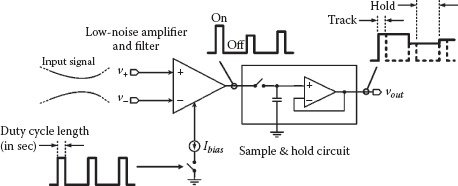
FIGURE 11.1 Simplified representation of a power scheduling strategy.
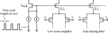
FIGURE 11.2 Simplified schematic of a current supply modulation scheme.
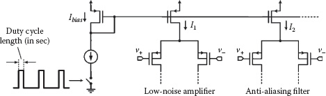
FIGURE 11.3 Simplified schematic of a duty cycling scheme.
Another technique, the multiplexing of several electrodes toward one low noise amplifier (LNA), has been demonstrated to save power and silicon area. Time division multiplexing of four channels toward a single neural amplifier is achieved in Chung-Ching, Zhiming, and Bashirullah [9]. In the proposed topology, a single LNA is shared between four independent input electrodes in order to decrease the power consumption per channel by four. A frequency division multiplexing (FDM) scheme is implemented in Joye, Schmid, and Leblebici [10], where the amplitude of the neural activity seen at several individual electrodes is modulated and directed toward a single wideband neural amplifier. These authors showed that the maximum number of electrodes that can be multiplexed toward a single amplifier is limited by the sum of the thermal noise from each electrode at the input node of the wideband neural amplifier, and it is in the range of 5 to 10 for typical cases.
On the other hand, activity-based schemes are exploiting the transient characteristics of neural signals to maximize efficiency. Adaptive sampling [11] is an activity-based technique that affords a significant decrease of the data rate by dynamically varying the sampling rate of an ADC, based on the input signal activity (Figure 11.4). Reduction factors of seven are reported with this scheme. The algorithm requires the implementation of the second derivative of the signal within dedicated circuits to measure the rate of change of the input. Other activity-based schemes exploit the intermittent nature of neural recordings along with their low duty cycles by powering up the recording building blocks only when neural events occur (Figure 11.5).
Such strategies require the utilization of accurate biopotential detectors along with power scheduling. In such schemes, most recording building blocks remain in an idle state, draining practically no current until neural events occur. In Gosselin and Sawan [12], a low overhead analog detector is employed to detect neural events and trigger the recording circuitry. Indeed, the approach proposed in Gosselin, Sawan, and Kerherve [13] is using low overhead analog delay elements that are implemented within ultralow power linear-delay filters to wake up the recording circuits “ahead” of biopotential occurrences, a critical behavior to avoid truncated waveforms.
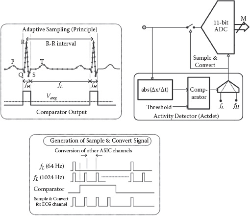
FIGURE 11.4 Architecture of an adaptive sampling analog-to-digital converter [11].
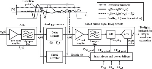
FIGURE 11.5 An activity-based scheme that is powering up the recording building blocks only when necessary. To decrease power consumption drastically, this strategy employs an accurate biopotential detector along with power scheduling [13].
Adaptive mechanisms have also been proposed for achieving high power efficiency. In such approaches, the DC operating points of a circuit are optimally adjusted by employing feedback. A neural amplifier using adaptive biasing is demonstrated in Sarpeshkar et al. [14]. This closed-loop scheme consists of indirectly adjusting the signal-to-noise ratio of an LNA by changing its bias current in order to set the input-referred noise of the amplifier right above the noise floor of the input electrode, thus avoiding any waste of energy.
11.2.3 ENERGY-EFFICIENT SENSORY CIRCUIT TOPOLOGIES
The LNA is the main building block of an analog front end; it must amplify and filter the neural waveforms in order to remove any input DC offset seen across a pair of differential electrodes, thereby maximizing the dynamic range in the recording channel. Indeed, it must provide sufficient gain, appropriate bandwidth, high signal-to-noise ratio (SNR), excellent linearity, and high common mode and high power supply rejection ratios (CMRRs and PSRRs) to provide the expected signal quality. In the case of a multichannel interface, one such sensory circuit per electrode is needed. Therefore, the LNA must consume little power and be of small size as well as scalable to multiple parallel channels. Furthermore, it is essential to optimize the design of the LNA for very low power through a dedicated circuit design methodology, as in Harrison and Charles [15]. The noise efficiency factor (NEF) has been widely adopted as a main figure of merit to assess the performance of LNAs and compare the several existing topologies together.
Designing sensory circuits that can capture multimodal neural information is critical to gather as much neural information as possible. Table 11.1 shows typical values of amplitude and bandwidth for different neural signals. Appropriate amplifiers can discriminate among multiple types of biopotentials by accommodating different frequency ranges [5,16,17]. They can provide different bandwidth settings by (1) tuning the resistive values in a filter, (2) selecting different capacitors values from an array, or (3) changing the operating points of a circuit. In several designs, the high-pass cutoff is changed by varying the gate voltage of a pseudoresistor [17,18] or that of a weakly inverted MOSFET (metal oxide semiconductor field-effect transistor) [19]. In contrast, the low pass cutoff is changed by varying the operating point of the LNA directly [15] or by changing its capacitive load through the selection of different output capacitors [7].
TABLE 11.1
Characteristics of Various Bioelectric Signals
Signal |
Bandwidth (Hz) |
Signal range (mVpp) |
Electrocardiogram (ECG) |
0.05 ~ 256 |
0.1 ~ 10 |
Electroencephalogram (EEG) |
0.001 ~ 100 |
0.01 ~ 0.4 |
Electrocorticogram (ECoG) |
0.1 ~ 64 |
0.02 ~ 0.1 |
Electromyogram (EMG) |
1 ~ 1 K |
0.02 ~ 1 |
Local field potential (LFP) |
0.001 ~ 200 |
0.1 ~ 5 |
Extracellular action potential (EAP) |
100 ~ 10 K |
0.04 ~ 0.5 |
However, tuneable circuits can present significant distortion and exhibit excessive process-dependent variations. Indeed, the resistance of the MOS devices is highly dependent on the voltage level of the output signal [18]. Dedicated linearization circuits have been proposed for performing appropriate biasing of the gate of a MOS device and linearizing the MOS resistor [1,18]. Such approaches have been extended further in Gosselin and Ghovanloo [8] by replacing any inaccurate current mirrors and source followers by precise closed-loop operational amplifiers, thus achieving high linearity above 74 dB within ±200 mV and enabling process-independent frequency cutoff values. This proposed strategy consists in linearizing a pseudoresistor by reporting any variations in the input voltage right at the gates of its constituting pMOS (positive metal oxide conductor) devices with unity gain. This maintains the gate to source voltage of the MOSFETs at constant value, thus canceling any nonlinearity, while providing adequate DC biasing to set the desired cutoff frequency.
A switched-capacitor neural amplifier with tuneable characteristics was recently demonstrated in Jongwoo, Johnson, and Kipke [20] as an alternative to conventional continuous-time circuits. In addition to providing low noise and satisfactory gain, this amplifier can accommodate local field potentials (LFPs) and action potentials (APs) through tuning of its clocking frequency, thus implementing different low- and high pass cutoff frequencies in a straightforward fashion.
11.2.4 A LOW POWER DISCRETE-TIME NEURAL INTERFACING FRONT END
An analog front-end topology employing a power scheduling strategy is presented. This approach aims at decreasing the average power consumption by leveraging duty cycling. The schematic of the front end is presented in Figure 11.6. In this scheme, an LNA providing a gain of 100 is powered up only for brief time intervals. The output of the LNA is sampled with a low power switched capacitor (SC) SHA circuit featuring an embedded low pass cutoff frequency for limiting the Johnson noise in the channel. This SHA circuit efficiently combines sampling action with low pass filtering in a compact building block. One challenge in the implementation of this duty cycling strategy is designing an LNA whose output can settle within a short time frame in order to provide high signal quality as well as low power. Indeed, wide bandwidth must be achieved in the LNA to allow fast settling, but this must be done without adding too much power overhead. The cutoff frequency of the LNA is set to 40 kHz, given a typical recording bandwidth of 8 kHz for extracellular AP. Indeed, the SHA circuit provides an embedded low pass cutoff frequency to limit the noise power below 8 kHz. Its simulated NEF was found to be as low as 1.3. The amplifier circuit is simulated using Cadence design tools and CMOS (complementary metal oxide semiconductor) 0.35 μm MOSFET models provided by the foundry. Table 11.2 summarizes the performance of the front end.
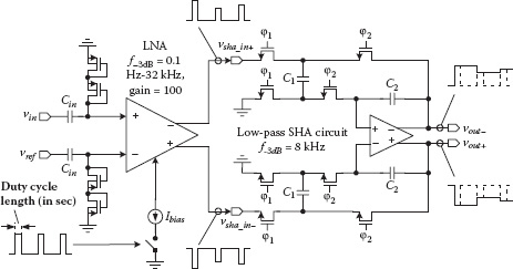
FIGURE 11.6 Analog front end employing duty cycling.
TABLE 11.2
Performance of the Analog Front End
Parameter |
Value |
Supply voltage |
1.8 V |
Power consumption |
<3 μW |
Gain |
100 V/V |
Input referred noise |
31 nV/√Hz |
Bandwidth |
1 mHz to 8 kHz |
Process |
CMOS 0.35 µm |
Source: B. Gosselin, The 33rd Annual International Conference of the IEEE Engineering in Medicine and Biology Society (EMBC’11), Boston, MA, pp. 5855–5859, 2011.
Before deriving the cutoff frequency of the SHA circuit, its z-transfer function will be obtained. Then, the continuous transfer function of the circuit will be derived from the z-transfer function, and the cutoff frequency of the SC-SHA will be calculated. We will use the single-ended representation of the circuit for simplicity, the schematic of which is shown in Figure 11.7.
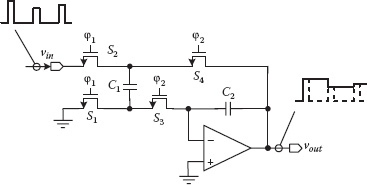
FIGURE 11.7 Single-ended form of the SHA circuit.
FIGURE 11.8 Equivalent representation of the circuit in sampling mode.
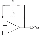
FIGURE 11.9 Equivalent representation of the circuit in holding mode.
First, in sampling mode (nT-T), when φ1 is high and φ2 is low, switches S1 and S2 are closed and C1 is charged to vin (Figure 11.8).
After this step, the expressions of the charges on C1 and C2 are as follows:
(11.1) |
(11.2) |
Then, in the holding mode (nT – T/2), when φ1 is low and φ2 is high, switches S3 and S4 are closed (Figure 11.9) and the charge on C1 is combined with the charge that is already present on C2. The resulting charge can be written as follows:
(11.3) |
We note that once φ1 turns off, the charge on C2 will remain the same during the next φ1, until φ2 turns on again in the next cycle. Therefore, the charge on C2 at time (nT), at the end of the next φ1, is equal to that at time (nT – T/2) or, mathematically,
(11.4) |
Then, vout can be obtained by combining (11.4) and (11.5), i.e.,
(11.5) |
Thus, vout of the SC-SHA will be
(11.6) |
The z-transfer function of the circuit is then derived as follows:
(11.7) |
To find the frequency response, we use z = ejωT in (11.7), which gives
(11.8) |
where the period T is the inverse of the clock frequency of the SC circuit fclk. The cutoff frequency of the SC circuit can be obtained from the denominator as follows:
(11.9) |
If the clock frequency is much higher than the highest frequency component of the signal (ωT ≪ 1), we can approximate e −jωT with the two first terms of its Taylor expansion. Therefore, the cutoff frequency at –3 dB will be approximately
(11.10) |
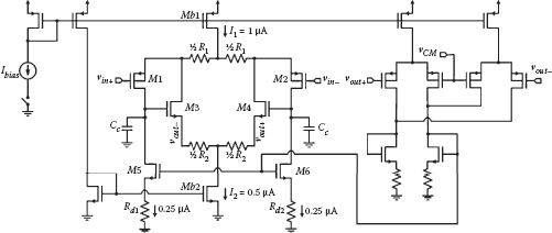
FIGURE 11.10 Schematic of an LNA employing duty-cycling.
The schematic of the wideband low power LNA along with its common-mode feedback (CMFB) circuit is presented in Figure 11.10. This design naturally features wide bandwidth since it employs only seven transistors, which implies minimum parasitic in the signal path. This, in turn, means that the overall power consumption of the LNA is solely determined by the required input-referred noise level. A transconductor (made of M1–M2, M5–M6, and R1) converts vin+ – vin– into a current, which is deflected, in part, into a transimpedance amplifier (made of M3–M4 and R2) and then translated into an amplified output voltage vout+ – vout–.
Then, an accurate and a simplified expression are obtained for the gain of the LNA. After that, the cutoff frequency of the LNA will be derived from this simplified gain expression. The half-circuit model of the LNA, the schematic of which is shown in Figure 11.11(a), is used to derive an expression for the gain.
From Figure 11.11(b), we can obtain the voltages at nodes Vx and Vy by writing the KCL equations at the different nodes. We first obtain i3 and i1, as illustrated in Figure 11.11(b).
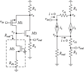
FIGURE 11.11 (a) Half circuit model of the LNA; (b) small signal model of the half circuit.
(11.11) |
and
(11.12) |
where rs1 corresponds to the inverse of gm1 in the T model of transistor M1. Then, voltage Vy is obtained as follows:
(11.13) |
where rs3 corresponds to the inverse of gm3 in the T model of transistor M3 and Rout is the equivalent resistance from the drain of M5. The latter is much larger than R1 and R2. Voltage Vy is obtained as follows:
(11.14) |
Then, we obtain the accurate gain expression of the LNA by writing
(11.15) |
Finally, we replace rs1 and rs3 with 1/gm1 and 1/gm3, respectively, and the gain expression of the LNA becomes
(11.16) |
We use the identity x + y + xy + 1 = (1 + x).(1 + y) to simplify (11.16). Assuming that
the gain expression then becomes
(11.17) |
Defining
the gain expression can be rewritten as
(11.18) |
If αR2 ≪ Rout, then the gain is approximately
(11.19) |
Denoting Cp the capacitor at node vy and knowing that αR2 ≪ Rout, we can write
thus yielding the 3 dB cutoff frequency of the LNA according to
(11.20) |
This design is using source degeneration resistors Rd1–Rd2 in the active load M5– M6 to decrease the contributed noise from these MOS devices, as in Wattanapanitch, Fee, and Sarpeshkar [17]. Moreover, split resistors R1–R2 are used along with a single current source in both differential pairs to cancel the second harmonic terms efficiently and achieve high linearity. The total current consumption of this optimized design can be very low since it features only three main branches and employs only seven transistors (not counting the CMFB and bias circuits). Furthermore, the utilization of source degeneration resistors in the MOS current mirror load is significantly lowering the overall input-referred noise. Also, the SHA circuit can be designed for very low power since the sampled signal is much less sensitive to noise after having been amplified by the LNA. For power consumption, the current drained from the power supply scales with the duty cycle length.
Indeed, using a duty cycle of 25% in this proposed design reduces the power consumption of the LNA by a factor of four. Similarly to a duty cycling arrangement, the same discrete-time front end can be incorporated into a TDM strategy where one common wideband LNA would be shared between several neural recording electrodes to save power. In such a configuration, the LNA must roughly provide n times the signal bandwidth (n × fmax) in order to process n TDM electrodes. For instance, the proposed LNA could enable the multiplexing of four neural recording electrodes with fmax = 8 kHz since its cutoff frequency is higher than four times the signal bandwidth (4 × fmax ≈ 32 kHz).
In this section, we have reviewed energy-efficient system-level architectures, smart power management strategies, and low power sensory circuit topologies that are improving efficiency in power-constrained multichannel recording arrangements. Moreover, the described strategies were illustrated through the design of a practical implementation—namely, a discrete-time neural recording front end employing duty cycling as a means to decrease its power consumption by 75%.
11.3 WAKE-UP RADIO FOR WIRELESS SENSOR NETWORKS
A wireless sensor network (WSN) is a collection of low cost, low energy computing devices, designated nodes or motes; each is equipped with one or more sensors, with limited computational and memory resources, that operate as a whole to accomplish a specific task. Typical applications include monitoring and data aggregation in fields including military, agricultural, medical, and environmental.
Two outstanding characteristics of WSNs are (1) the ad hoc, self-organized, and self-healing nature of the network, and (2) the extremely low energy budget each sensor node is allocated. The latter constraint is due in part to the small size and cost of the nodes, which leaves little room for bulky batteries, and also to the nature of the applications, which require the nodes to remain operational for months, perhaps years after initial deployment without human intervention. Energy sources include small batteries and energy scavenging mechanisms (solar, mechanical vibrations, heat). In the case of batteries, which is by far the more common solution, the useful life of the network is limited by the first node failure, so network protocols are typically designed to ensure that all nodes are equally active so that their batteries are drained at an equal rate.
The power consumption of the individual nodes is therefore a topic of the highest importance, which tends to be dominated by the RF transmit and receive functions in the vast majority of applications. Any subsystem of a node that is not needed momentarily is typically put in sleep mode, and the RF subsystem is no exception.
Various techniques have been devised to allow a node to “wake up” only when it needs to transmit and/or receive a data packet and then go back to sleep once its task is complete. In typical operation, nodes can acquire data from their sensor at periodic intervals, process this data locally (feature extraction, data compression, etc.), forward the data, relay packets that are meant for another node or for the base/aggregation station, or receive query/command packets. Multihop packet relaying is favored because it is more energy efficient than transmitting in a single hop over a larger distance.
To allow nodes to be in deep sleep (including the RF section) most of the time, thus consuming minimal power, typically requires protocols that operate in a synchronous or pseudosynchronous manner to ensure that nodes that need to communicate are awake at the same time [22]. In synchronous operation, the whole network wakes up at periodic intervals; performs whatever acquisition, processing, and communication tasks are required; and then goes back to sleep. In pseudosynchronous or rendezvous protocols, nodes attempt to predict at what moment they will be needed and should wake up based on past history. In effect, the network as a whole attempts to establish a dynamic optimum schedule in a totally distributed manner. This obviously implies additional processing (and possibly signaling) overhead to determine the continuously changing sleep interval, as well as missed rendezvous and false-alarm wake-ups. In the end, no matter how sophisticated the rendezvous protocol is, the receive sections of nodes have to stay awake significantly longer than the packet duration in order to have a fair chance of making the rendezvous. For this reason, the RF receive function typically dominates the power consumption budget in WSN, even though its instantaneous consumption is less than the transmit function.
11.3.1 THE WAKE-UP RADIO CONCEPT
The preceding discussion highlights how desirable it is to minimize the on-time of the RF receive functions and, if possible, to avoid the complications of rendezvous protocols. The only remaining option—totally asynchronous operation—requires a means to “wake up” a node remotely on demand, using only an RF signal. Forgoing the need to have the network maintain a communication schedule, each node is equipped with an ultra low power wake-up radio (WUR), which continuously monitors the channel. This is in addition to the main RF transceiver unit, which can therefore be turned off most of the time. When a node wishes to communicate with a neighbor, it sends a wake-up signal, containing the wake-up code or address of the target, thus waking only the desired node (see Figure 11.12). After successful reception and address decoding of the wake-up signal, the WUR brings the entire node out of sleep mode if the wake-up code matches one of the node’s wake-up codes. An acknowledgment packet is then sent to signal the first node that transmission can proceed. After the data exchange is complete and after any additional tasks are performed, both nodes can go back to sleep, activating their WUR before doing so.
For asynchronous operation to be effective and competitive with rendezvous protocols, the power consumption of the wake-up device must be extremely low. It has been estimated that the wake-up radio must have a power consumption below 50 μW in order to constitute an attractive alternative [23] and should be below 10 μW to extend the range of WSN applications [24]. In a 2010 survey [25], the feasibility requirements of wake-up radios were listed: low cost, low power usage, low latency, low interference, low missed wake-up rate, and appropriate range (with a typical goal of 10 m). As of 2010, no reported implementation meets all these requirements and very few complete, stand-alone, and working implementations have been reported to date.
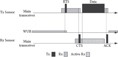
FIGURE 11.12 Example of asynchronous operation presenting a wake-up, acknowledge, and receive wake-up behavior. (a) Transmission of the wake-up code. (b) Reception and processing of the wake-up code and possible wake-up of the node. (c) Acknowledgment of wakeup. (d) Data transmission and return to sleep mode.
Restricting our attention to complete, fully functional sensor nodes, the first reported wake-up radio (in 2007) is described in Van der Doorn, Kavelaars, and Langendoen [26]. Since it is built from off-the-shelf components (including a microcontroller) and consists of a wake-up radio piggyback board in conjunction with Delft University’s T-node platform, the power consumption in practice is quite high—above 600 μW, although the design could, in principle, have operated at 170 μW after resolution of certain practical issues. Furthermore, the range was only 2–3 m. It follows that while this is a conceptually compelling first effort, its interest is mostly academic.
Examples of the current state of the art include the design reported by Ansari, Pankin, and Mähönen in 2008 [27] and that of Hambeck, Mahlknecht, and Herndl in 2011 [28]. Based on the Telos node, the design in Ansari et al. [27] uses a secondary radio in the 868 MHz band to transmit the wake-up signal, thus shifting some of the complexity and power burden to the transmitter. The receiver employs impedance matching and a five-stage voltage multiplier, resulting in a wake-up circuit that consumes only 876 nA. The entire node in sleep mode consumes 12.5 μW, which is significantly below the 50 μW barrier. However, the observed range is of the order of 2.5 m, thus falling short of the 10 m objective.
Hambeck et al. [28] report a wake-up radio chip implementation in 130 nm CMOS leveraging various low power techniques to achieve a consumption of 2.4 μW (wake-up unit only) and a sensitivity of –71 dBm at 868 MHz. However, it seems that this extraordinary sensitivity is obtained in part by correlating over very long sequences, thus trading off wake-up time for sensitivity and possibly shifting part of the power burden to the transmitter. In fact, the paper cites a wake-up time of 40 to 110 ms, which is enormous, and the extraordinary receiver sensitivity is based on correlation over a 7 ms period (thus accumulating energy) with an external surface acoustic wave (SAW) filter.
11.3.2 A LOW POWER WUR DESIGN BASED ON PWM
It has been established previously that in assessing the quality of a WUR design, multiple variables must be taken into consideration in addition to receiver sensitivity and power consumption, such as wake-up time, bit rate, robustness to interference, range, band of operation, the completeness of the design, etc. As a case study, we examine a design dating from 2008 [29,30] that presents some unusual and innovative characteristics.
The vast majority of reported wake-up radio designs operate at a frequency of 868 MHz, including the latest state-of-the-art ones [27,28]. This allows better range and/or lower power consumption compared with higher frequency bands such as the popular 2.4 GHz unlicensed band. However, it should be noted that 868 MHz does not constitute a globally available band. It is an unlicensed band in Europe, but not in North America (where the ISM band is at 908 MHz instead). Furthermore, while path loss is lower at 868 MHz, antenna gain is also lower and/or antenna size is larger than at 2.4 GHz. It follows that for compact nodes with decent antenna gains and for designs that can operate globally, 2.4 GHz is a better option.
Aside from operating in the 2.4 GHz band, the design under study also features a highly unusual modulation format. Indeed, nearly all surveyed WUR implementations leverage on/off keying (OOK) for simplicity of operation, while the design under study is based on pulse-width modulation (PWM). This is arguably the central innovation of this design, as this choice leads to many benefits. To the best of our knowledge, this modulation has not been used before in single-chip wake-up radio implementations, although an early effort from off-the-shelf components has been reported [31], where PWM was used specifically to alleviate complex synchronization requirements.
First, we observe that both OOK and PWM are forms of amplitude modulations that are amenable to mostly passive, extremely simple receiver structures based on, for example, an envelope detector and an integrator. Second, unlike OOK, the PWM is self-synchronizing (since there is a pulse for every transmitted bit) and does not require sophisticated clock recovery circuitry. Third, PWM allows arbitrary control of the duty cycle. For example, choosing to transmit zeros as 3 μs pulses and ones as 12 μs pulses, and assuming a symbol period of 20 μs, the mean duty cycle (with equiprobable bits) is 37.5%. This leads to transmit energy savings with respect to constant envelope (frequency and/or phase modulation, duty cycle of 100%) and OOK (duty cycle of 50%).
The fourth and possibly most important benefit of PWM is its natural robustness to both noise and interference. Indeed, because the information is encoded in the duration of the pulses, the effect of additive white Gaussian noise is different, thus leading to higher resistance [32,33]. Additionally, because this modulation is radically different from that of other modulation types used by interfering signals and its detection is based on pulse duration, it is also robust to interferers.
It is noteworthy that PWM has been forgotten for a long time as a wireless form of modulation because it is inherently not bandwidth efficient. However, bandwidth efficiency is not a primary concern in the unusual context of wireless sensor networks.
The WUR circuit architecture is depicted in Figure 11.13. The RF detector is a form of envelope detector—more specifically, a zero-bias Schottky diode voltage doubler. Impedance matching is integrated into this component with lumped reactive elements in order to minimize the form factor. This matching is optimized for a subset of the 2.4 GHz ISM band, with a worst-case return loss of –10 dB for the first six 802.11 channels (out of 14).
The amplifier is by far the most power-hungry block of the WUR reception chain. It consists of a two-stage structure (see Figure 11.14) providing an approximate gain of 86 dB for a bandwidth of 180 kHz. A Schmitt trigger inverter at the output provides digitization prior to entering the PWM demodulator.
PWM modulation is performed by an asymmetrical inverter followed by a capacitor, the pair acting as a resettable integrator. Transistors are sized to determine integration time constants such that pulses shorter than 10 μs yield a logical zero and longer pulses yield a logical one. A symbol-rate clock is generated along with the main output of the integrator, and both signals are passed to the shift register.
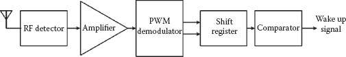
FIGURE 11.13 Architecture of PWM-based wake-up radio. The antenna is not necessarily dedicated to the wake-up device; it can be shared with the main transceiver. The RF detector provides a baseband signal to the demodulator. The amplitude modulation used is PWM since it provides clocking information. The received information is fed to a shift register and its content is compared to the node’s address, generating a wake-up signal if there is a match.
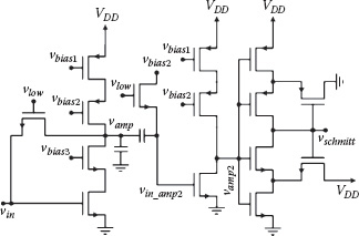
FIGURE 11.14 Two-stage amplifier structure with Schmitt trigger output.
The shift register is 8 bits long and, together with the comparator, allows matching with a local unique 8-bit address. Thus, only wake-up radio signals targeted at this specific node will be recognized and activate the wake-up line to the core of the node.
The proposed WUR circuit, consisting of a layout in 130 nm CMOS using an IBM process, was validated through SPICE simulation given a 50 kHz PWM signal having a 15% duty cycle for zeros and a 60% duty cycle for ones. It was seen that the device functions adequately with a sensitivity of –55 dBm. This is deemed to correspond to a practical range of between 4 and 5 m for propagation exponents between two and three.
The breakdown of the power consumption per component is given in Table 11.3. It can be seen that all components except the amplifier consume negligible power, thus providing a clear path for further improvement in this respect. With a 1 V power supply, the entire circuit (in simulation) consumes 10 μA.
It is noteworthy that addresses longer than 8 bits could be used with minimal impact on the power budget. Only the current drawn by the comparator stage would change, in a manner that is linear with the address length.
The range could also be substantially increased by making use of directional antennas. One possible scenario involves equipping a node with four directional antennas of moderate gain pointing 90° away from each other with patterns that are wide enough to collectively cover 360° in azimuth adequately. This could provide a gain of approximately 6 dB or more, depending on how directive the antennas are in elevation. A similar gain could be obtained at the transmitter (for a total gain of 12–15 dB) if the transmitter “knows” in what direction the target node is (a likely hypothesis, provided the network is capable of geographic self-discovery and self-organization).
Two possible schemes can be devised to integrate such a four-antenna layout with a wake-up radio. In the first scheme, a single WUR circuit is shared by all four antennas. A switching mechanism connects it to a single selected antenna out of the set of four. A continuously running timer would trigger a switching event at regular intervals so that all four antennas are listened to in turn. This has the benefit of requiring only one complete WUR circuit, albeit at the cost of slightly increased complexity and power consumption (the timer and switching mechanism) and a higher chance of missed wake-ups.
TABLE 11.3
Per-Component Breakdown of the Average Power Consumption of the WUR circuit with 15%/60% Duty Cycle 50 kHz PWM Signal
Building block |
Average consumption with 50 kHz signal and noise (µW) |
Average consumption with noise only (pW) |
RF detector |
0 |
0 |
Amplifier |
17.80 |
18.29 |
PWM demodulator |
0.8 |
0.06 |
Address decoder |
0.02 |
<0.01 |
Total |
18.61 |
18.35 |
In the second scheme, a full WUR circuit is implemented for each antenna so that wake-up signals from any direction can be intercepted at any time. Obviously, the power consumption of this scheme would be much higher. However, it has been observed that most of the power consumption (60%) is in the amplifier bias circuitry. Since this circuitry can be shared among all four WUR components, it can be assumed that the overall power consumption would be (60% + 4 × 40%) × 19 μW = 2.2 × 19 μW = 41.8 μW, which is still below the 50 μW threshold.
This demonstrates that the multiple antenna context is feasible, especially in light of potential improvements in the amplification section to make it more power efficient.
Throughout this section, we have surveyed the state of the art in wake-up radio circuit design as a means to achieve fully asynchronous ultralow power wireless sensor networks. We have also presented a complete stand-alone wake-up radio architecture that, in the form of a layout in 130 nm CMOS, provides an overall power consumption of less than 19 μW in the 2.4 GHz band and with a sensitivity on the order of –55 dBm. This demonstrates that the wake-up radio concept is both feasible and useful, since the power consumption is far below the 50 μW usefulness threshold agreed upon in the literature. Furthermore, ideas could be borrowed from recently reported designs with even lower power consumptions (although they operate at 868 MHz instead of 2.4 GHz) to improve the reviewed architecture. The notion of using multiple directive antennas in order to achieve directive gain and thus greater range and/or RF energy savings was also discussed.
1. Z. Xiaodan, X. Xiaoyuan, Y. Libin, and L. Yong, A 1 V 450 nW fully integrated programmable biomedical sensor interface chip. IEEE Journal Solid-State Circuits, vol. 44, pp. 1067–1077, 2009.
2. A. Bonfanti et al., A multi-channel low-power system-on-chip for single-unit recording and narrowband wireless transmission of neural signal. Annual International Conference of the IEEE Engineering in Medicine and Biology Society (EMBC’10), pp. 1555–1560, 2010.
3. A. M. Sodagar, K. D. Wise, and K. Najafi, A wireless implantable microsystem for multichannel neural recording. IEEE Transactions on Microwave Theory and Techniques, vol. 57, pp. 2565–2573, 2009.
4. B. Gosselin et al., A mixed-signal multichip neural recording interface with bandwidth reduction. IEEE Transactions on Biomedical Circuits and Systems, vol. 3, pp. 129–141, 2009.
5. L. Seung Bae, L. Hyung-Min, M. Kiani, J. Uei-Ming, and M. Ghovanloo, An inductively powered scalable 32-channel wireless neural recording system-on-a-chip for neuroscience applications. IEEE Transactions on Biomedical Circuits and Systems, vol. 4, pp. 360–371, 2010.
6. X. Zhiming, T. Chun-Ming, C. M. Dougherty, and R. Bashirullah, A 20 μW neural recording tag with supply-current-modulated AFE in 0.13 μm CMOS. IEEE International Solid-State Circuits Conference (ISSCC’10), pp. 122–123, 2010.
7. M. S. Chae, Z. Yang, M. R. Yuce, L. Hoang, and W. Liu, A 128-channel 6 mW wireless neural recording IC with spike feature extraction and μWB transmitter. IEEE Transactions Neural Systems Rehabilitation Engineering, vol. 17, pp. 312–321, 2009.
8. B. Gosselin and M. Ghovanloo, A high-performance analog front-end for an intraoral tongue-operated assistive technology. IEEE International Symposium on Circuits and Systems (ISCAS), pp. 2613–2616, 2011.
9. P. Chung-Ching, X. Zhiming, and R. Bashirullah, Toward energy efficient neural interfaces. IEEE Transactions Biomedical Engineering, vol. 56, pp. 2697–2700, 2009.
10. N. Joye, A. Schmid, and Y. Leblebici, Extracellular recording system based on amplitude modulation for CMOS microelectrode arrays. IEEE Biomedical Circuits and Systems Conference, pp. 102–105, 2010.
11. R. F. Yazicioglu, K. Sunyoung, T. Torfs, K. Hyejung, and C. Van Hoof, A 30 μW analog signal processor ASIC for portable biopotential signal monitoring. IEEE Journal Solid-State Circuits, vol. 46, pp. 209–223, 2011.
12. B. Gosselin and M. Sawan, Circuits techniques and microsystems assembly for intracortical multichannel ENG recording. IEEE Custom Integrated Circuits Conference (CICC’09), pp. 97–104, 2009.
13. B. Gosselin, M. Sawan, and E. Kerherve, Linear-phase delay filters for ultra-low-power signal processing in neural recording implants. IEEE Transactions on Biomedical Circuits and Systems, vol. 4, pp. 171–180, 2010.
14. R. Sarpeshkar et al., Low-power circuits for brain–machine interfaces. IEEE Transactions on Biomedical Circuits and Systems, vol. 2, pp. 173–183, 2008.
15. R. R. Harrison and C. Charles, A low-power low-noise CMOS amplifier for neural recording applications. IEEE Journal Solid-State Circuits, vol. 38, pp. 958–965, 2003.
16. M. Mollazadeh, K. Murari, G. CauWenberghs, and N. Thakor, Micropower CMOS integrated low-noise amplification, filtering, and digitization of multimodal neuropotentials. IEEE Transactions on Biomedical Circuits and Systems, vol. 3, pp. 1–10, 2009.
17. W. Wattanapanitch, M. Fee, and R. Sarpeshkar, An energy-efficient micropower neural recording amplifier. IEEE Transactions on Biomedical Circuits and Systems, vol. 1, pp. 136–147, 2007.
18. Y. Ming and M. Ghovanloo, A low-noise preamplifier with adjustable gain and bandwidth for biopotential recording applications. IEEE International Symposium on Circuits and Systems (ISCAS’07), pp. 321–324, 2007.
19. P. Mohseni and K. Najafi, A fully integrated neural recording amplifier with DC input stabilization. IEEE Transactions on Biomedical Engineering, vol. 51, pp. 832–837, 2004.
20. L. Jongwoo, M. D. Johnson, and D. R. Kipke, A tunable biquad switched-capacitor amplifier-filter for neural recording. IEEE Transactions on Biomedical Circuits and Systems, vol. 4, pp. 295–300, 2010.
21. B. Gosselin, Approaches for the efficient extraction and processing of neural signals in implantable neural interfacing microsystems. The 33rd Annual International Conference of the IEEE Engineering in Medicine and Biology Society (EMBC’11), Boston, MA, pp. 5855–5859, 2011.
22. H. Carl and A. Willig, Protocols and architectures for wireless sensor networks. Chichester, England: Wiley, 2007.
23. E.-Y. Lin, J. Rabaey, and A. Wolisz, Power-efficient rendezvous schemes for dense wireless sensor networks. Proceedings ICC (IEEE International Conference Communications), pp. 3769–3776, 2004.
24. M. Spinola Durante, Wakeup receiver for wireless sensor networks, PhD dissertation, Institute of Computer Technology, Vienna, University of Technology, Vienna, Austria, 2009.
25. B. Kersten and C. G. U. Okwudire, MAC layer energy concerns in WSNs: Solved? Unpublished research paper, SAN (System Architecture and Networking) Group Seminar, TU Eindhoven, Feb. 2010.
26. B. Van der Doorn, W. Kavelaars, and K. Langendoen, A prototype low cost wakeup radio for the 868 MHz band. International Journal Sensor Networks, vol. 5, no. 1, pp. 22–32, 2009.
27. J. Ansari, D. Pankin, and P. Mähönen, Radio-triggered wake-ups with addressing capabilities for extremely low power sensor network applications. Proceedings PIMRC (IEEE International Symposium on Personal, Indoor, Mobile and Radio Communications), pp. 1–5, 2008.
28. C. Hambeck, S. Mahlknecht, and T. Herndl, A 2.4 μW wake-up receiver for wireless sensor nodes with –71 dBm sensitivity. Proceedings ISCAS (IEEE International Symposium on Circuits and Systems), pp. 534–537, 2011.
29. P. Le-Huy and S. Roy, Low-power 2.4 GHz wake-up radio for wireless sensors. Proceedings WiMob (Wireless Mobility Conference), pp. 13–18, 2008.
30. P. Le-Huy and S. Roy, Low-power wake-up radio for wireless sensor networks. Mobile Networks and Applications, vol. 15, no. 2, pp. 226–236, April 2010.
31. S. von der Mark et al., Three stage wakeup scheme for sensor networks, Proceedings International Conference on Microwave and Optoelectronics, pp. 205–208, 2005.
32. H. S. Black, Modulation theory. New York: Van Nostrand, 1953.
33. A. B. Carlson, Communication systems, 4th ed. New York: McGraw–Hill, 2002.