
An Open-Loop Multiphase Local-Oscillator Generation Technique |
|
CONTENTS
12.2 Overview of Multiphase LO Generation
12.3 Mathematical Model of Open-Loop Multiphase LO Generator
12.3.1 Four-Phase LO Generation
12.3.2 Eight-Phase LO Generation
12.4 Practical Design Considerations
12.4.3 Design and Verification Flow
12.5 Design Example: A Four-/Eight-Phase LOG for a Mobile TV Receiver in 65 nm CMOS
Multiphase local-oscillator (LO) generators are widely employed in modern wire-less/wireline communication systems. This chapter describes how an inverter-based open-loop four-/eight-phase LO generator can be utilized to cover a wide spectrum and relax the speed requirement of the phase-locked loop (PLL) and voltage-controlled oscillator (VCO), when comparing with the conventional frequency-divider-based method. The mathematical models of open-loop four-phase and eight-phase LO generators are developed. A design example targeting the mobile TV applications is implemented in 65 nm CMOS (complementary metal oxide semiconductor) technology to prove the feasibility of the technique. It covers the full band (VHF-III, UHF, and L) of mobile TV with two operating modes (i.e., the eight-phase mode supports image reject down-conversion whereas the four-phase mode supports typical quadrature down-conversion).
12.2 OVERVIEW OF MULTIPHASE LO GENERATION
Many different types of multiphase LO/clock generators have been reported for wireless and wireline applications. A ring VCO based on CMOS inverters (Figure 12.1a) is a compact solution to realize a multiphase LO with a large frequency range [1,2]. However, its phase noise performance is normally unacceptable for high-tier wireless systems. Although the phase noise can be substantially reduced by replacing all inverters with LC VCOs (Figure 12.1b), the associated inductors occupy a significant part of the chip area [3,4]. Delay-locked loop (DLL) using numerous delay units can also be a multiphase clock generator (Figure 12.1c) [5,6]. The key drawback is that the phase-noise performance is heavily dependent on the number of output phases required.
Alternatively, a multiphase LO signal can be generated in an open-loop way by using a low noise LC VCO followed by a frequency divider (Figure 12.1d). Elementarily, a four-phase LO can be generated via a div-by-2 circuit. Such a division factor implies that the associated PLL and VCO have to operate at a doubled frequency. The design complexity, however, rises dramatically with the number of phases required. For instance, to generate an eight-phase LO, a div-by-4 circuit is necessary; the PLL and VCO have to operate at four times the output frequency. A higher operating frequency unavoidably calls for more power to lower the phase noise and phase error. Moreover, the PLL and VCO will be more sensitive to parasitic capacitances, implying narrower locking and tuning ranges, respectively. To surmount these constraints, the frequency divider can be replaced by a passive RC-CR polyphase filter (Figure 12.1e) [7,8], but the performance can be strongly affected by the temperature and process variations, while power-hungry buffers are required for proper interface.
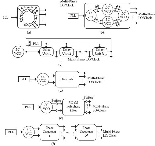
FIGURE 12.1 Multiphase LO/clock generation methods: (a) ring with inverters, (b) ring with LC VCOs, (c) DLL, (d) frequency divider, (e) RC-CR polyphase filter, and (f) phase correctors in cascade.
Recently, an open-loop four-phase clock generator was proposed for wireline applications [9,10]. Multiple phase correctors are cascaded in an open-loop way to improve the phase precision (Figure 12.1f). The prime advantages of this method are its simplicity (i.e., open loop and inverter only), no power-hungry buffer, and that the number of output phases is independent of the operation frequency of the circuit itself and its driving source. The achieved frequency range in Kim et al. [9] is 0.37 to 2.5 GHz and the phase precision is ±5° for a four-phase output.
In this content, we extend the concept of such open-loop architecture for wireless applications with different requirements on the phase precision and the number of output phases [11,12]. The targeted phase error is ±1° and both four- and eight-phase LO generators will be designed and analyzed.
12.3 MATHEMATICAL MODEL OF OPEN-LOOP MULTIPHASE LO GENERATOR
12.3.1 FOUR-PHASE LO GENERATION
12.3.1.1 Architecture
The block diagram of a four-phase LO generator is depicted in Figure 12.2. It is structured by putting numerous phase correctors in cascade to interpolate a four-phase LO from a two-phase differential input (vclk and vclkp). From left to right, the phase correctors improve the phase precision progressively until reaching the desired accuracy. The schematic of each inverter-based quadriphase corrector is shown in Figure 12.3. Every corrector is composed of 16 inverters (CMOS) classified according to two different device sizes as L-type or S-type. L-type inverters feature a larger geometrical size than the S-type to optimize the phase precision in a specific frequency range. The inverters can be divided into three groups according to their functionality:
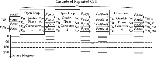
FIGURE 12.2 Block diagram of a four-phase LO generator. Phase error is reduced down progressively from the correctors 1 to N.
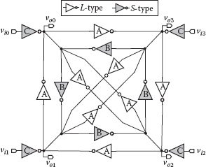
FIGURE 12.3 Architecture schematic of an inverter-based four-phase corrector.
• Set A is for phase correction. With three inverters in a loop, it is able to oscillate and interpolate the intermediate phases.
• Set B is for natural-frequency suppression. It leads to a larger operating frequency range [16].
• Set C is for signal injection. It allows multiple phase correctors to be cascaded directly to improve the output phase precision.
12.3.1.2 Mathematical Model
In order to determine the optimum conditions in terms of frequency range and phase precision, the four-phase corrector is modeled by a signal flow graph (SFG) as shown in Figure 12.4. For simplicity, a linear model is assumed [13,14]. Each inverter is modeled as a single-pole amplifier with a transfer function of h(f) as given by
(12.1) |
where G is the normalized DC gain and fC is the –3 dB cutoff frequency. The constants a and b in Figure 12.5 represent the driving capability of L-type and S-type inverters, respectively.
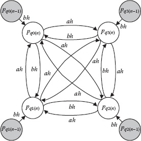
FIGURE 12.4 SFG of a four-phase corrector.
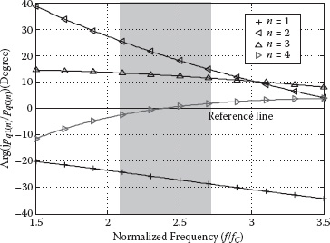
FIGURE 12.5 Static phase error of four-phase corrector with a/b = 3.4 and G = 10 (linear model simulation).
Phasor-domain analysis is applied to obtain the phase correction transformation of the nth phase corrector as expressed by
(12.2) |
where Aq is the phase transformation matrix and pq(n) is the output phase vector. Rearranging (12.2) yields
(12.3) |
For N quadriphase cascaded correctors, pq(N) becomes
(12.4) |
where pq(0) is the input phase vector represented by
(12.5) |
since the input phase can be either 0° or 180°. In the phasor domain only 1 or –1 is available for the input vector. Figure 12.5 shows the steady-state phase error function defined by (12.6) with a different number of stages in cascade
(12.6) |
where a/b is chosen to be 3.4 to provide an acceptable frequency range and G is selected as 10 (practical DC gain value of a CMOS inverter in nanometer technologies). The steady-state phase error depends on the ratio of the output frequency (f) to the corner frequency of an inverter (fc), as well as the number (n) of phase correctors in cascade. With n = 4, the phase error is minimized over a wide range of f/ fc (between 2.1 and 2.7). Figure 12.5 also shows that the steady-state phase error can be minimized by cascading additional stages of four-phase correctors for certain frequency ranges.
Based on the preceding definitions and following a particular context, the transfer function of the linearized quadriphase LO generator will be derived next. According to it, the optimal conditions for minimizing the phase error are obtained to build up the device-sizing strategy. From (12.2), we can simply prove that
(12.7) |
Thus, (12.2) and (12.3) can be simplified as
(12.8) |
And also for a simplification of the notations, A, B, and C are introduced as follows:
(12.9) |
Similarly to (12.4), we can obtain
(12.10) |
Since the matrix C can be diagonalized as
(12.11) |
substituting it in (12.10) will finally lead to
(12.12) |
Finally, the transfer function of pq1(N) divided by pq0(N) can be obtained as
(12.13) |
The criteria for phase error minimization are equivalent to set
(12.14) |
which implies a 90° phase shift. Substituting (12.14) into (12.13) leads to
(12.15) |
By solving (12.15) the optimal conditions for phase error minimization can be obtained as
(12.16) |
This implies that an ideal 90° phase shift happens at the natural frequency of the circuit: fn = G(a − b) fc. Also, a larger a/b ratio can provide a stronger phase-correcting ability.
12.3.2 EIGHT-PHASE LO GENERATION
12.3.2.1 Architecture
Eight-phase LO generation can be obtained by further extending the four-phase LO concept and architecture previously outlined. As such, the block diagram of an eight-phase LO generator can be drawn as illustrated by Figure 12.6. From left to right, an eight-phase LO can be composed of multiple octave-phase correctors. The number of stages in cascade will directly depend on the final phase-precision requirement. The architecture schematic of an eight-phase corrector is shown in Figure 12.7, which is composed of 32 inverters (CMOS). Similarly to the four-phase design, the inverters are also classified as L-type or S-type and the three sets (A, B, and C) previously mentioned are also maintained.
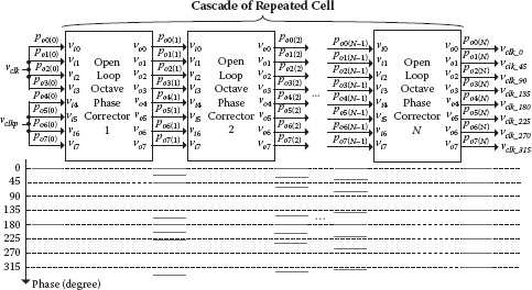
FIGURE 12.6 Block diagram of an eight-phase LO generator.
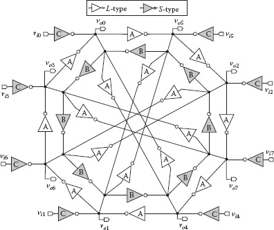
FIGURE 12.7 Architecture schematic of an eight-phase corrector.
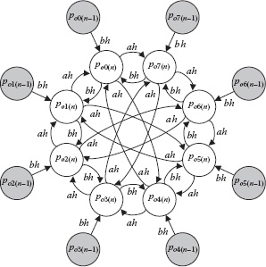
FIGURE 12.8 SFG of an eight-phase corrector.
12.3.2.2 Mathematical Model
The SFG of the eight-phase corrector is presented in Figure 12.8, where a linear model is also assumed and each inverter is modeled, similarly, as a single-pole amplifier. Again, phasor-domain analysis is applied to obtain the phase transformation of the nth octave-phase corrector as given by
(12.17) |
where Ao is the octave-phase transformation matrix and po(n) is the output phase vector of the nth octave-phase corrector. Rearranging (12.17) will yield
(12.18) |
For N octave-phase correctors in cascade, po(N) is given by
(12.19) |
where po(0) is the input phase vector
(12.20) |
since the input phase can be either 0° or 180°. In the phasor domain, only 1 or –1 is available for the input phase vector. The steady-state phase error function can be defined by
(12.21) |
As illustrated by Figure 12.9, the steady-state phase error can be minimized by cascading additional stages of octave-phase correctors for a certain frequency range from 0.7 to 1.3 (normalized frequency: f/fc). The a/b ratio is set to be 3.5 and G is 10. Although the optimum conditions in terms of frequency range and phase precision can be derived from the linear model, the final phase permutation can only be determined from transistor-level simulation because not all the transistors can be operated, simultaneously, in the saturation region.
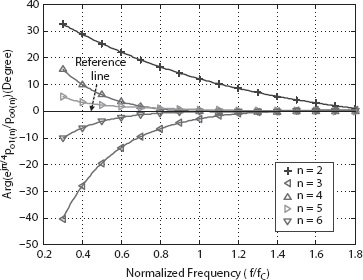
FIGURE 12.9 Static phase error of octave-phase corrector with a/b = 3.5 and G = 10 (linear model simulation).
12.4 PRACTICAL DESIGN CONSIDERATIONS
Both quadri- and octave-phase correctors have a limited operating frequency range. The channel length of the inverter’s transistors is correlated to the upper frequency limit (i.e., a smaller channel length allows a higher operating frequency). When the channel length is fixed, the a/b ratio is correlated to the range and the phase-correcting ability of the phase corrector. A smaller a/b ratio can increase its operating range at the expense of a weaker phase-correcting ability. Thus, subject to different applications, the optimum a/b ratio should be chosen such that the desired frequency range can be covered. On the other hand, the optimum number of phase correctors needed in cascade can be determined according to the required phase precision.
Similarly to the ring oscillator, the frequency range covered by the phase corrector can be sensitive to process, voltage, and temperature (PVT) variations. For fast-fast (FF)/slow-slow (SS) process corner with temperature and voltage variations, the covered frequency range is shifted up or down significantly. For a reliable design, the channel length of the inverters is determined at “SS corner + low supply voltage + high temperature” for the highest operating frequency to be larger than the desired frequency. Then, a suitable a/b at “FF corner + high supply voltage + low temperature” is chosen for the lowest operating frequency, which is also lower than the desired frequency. Increasing the width of the transistors can only lead to a better variability control at the expense of power. The operating principle is not dependent on the transistors’ width.
12.4.3 DESIGN AND VERIFICATION FLOW
The design and verification flow is graphically summarized in Figure 12.10(a) and (b). For simplicity, only the quadriphase LO generator is considered. Based on the developed linear model and equations, the phase error vector can be determined with initial values of G, a/b ratio, and n. These values can be adjusted to minimize the phase error over the desired frequency range with fast simulation speed. The obtained circuit parameters are then transferred to the transistor-level design. Since the circuit is dynamic, the optimization involves mostly transient simulations—except for the particular case of the phase noise, which was checked through periodic noise (pnoise) simulations. Although the linear model can provide a set of parameters that are close to the optimum values, transistor-level fine tuning is still necessary to account for PVT variations. Circuit nonlinearity may also affect the final phase permutation and it must be confirmed at transistor level. Finally, the optimized circuit can be transferred to the layout design phase. Postlayout verification with parasitic effects is needed to reconfirm all performance metrics and it will be repeated until all specifications are met.
12.5 DESIGN EXAMPLE: A FOUR-/EIGHT-PHASE LOG FOR A MOBILE TV RECEIVER IN 65 NM CMOS
A four-/eight-phase LOG was fabricated with a mobile TV receiver in 65 nm CMOS [15,16]. The entire scheme is shown in Figure 12.11. It is based on two chains of eight-phase corrector (8PC) for achieving harmonic rejection (HR) in the VHF-III and UHF bands, and one chain of four-phase corrector (4PC) for simple quadrature down-conversion in the L-band. A high-level algorithm has been developed in MATLAB to optimize the device size, number of stages, and frequency range using the developed linearized model. This dedicated coverage lowers the tuning range of each phase corrector chain, thereby lowering the phase error. The entire LOG is implemented with thin-oxide MOSFETs (metal-oxide semiconductor field-effect transistors) operating at a 1.2 V supply. Selectors with a logic arrangement feature assign the correct LO phase to each mixer in different modes.
The injection signal LOin might cover the desired bands by using a 1.27 to 1.92 GHz PLL + VCO (not integrated in this work) with selectable output division ratios (1, 2, 3, 6, and 8). The required division ratios can be of any number as they are unrelated to the phases of LOout. In the L-band, the PLL + VCO works at the same RF frequency. The phase precision of the LOG is mainly limited by the routing in the layout, where the transistor intrinsic RC value is sensitive to the parasitics. The LOG was laid out and extracted to tune out this effect in several iterations. In the postlayout simulation (PLS), the phase error for eight-phase output is optimized to be <1° for the VHF-III and UHF bands. This precision fairly meets our target of HR ratio of 33 dB, even under a possible gain mismatch up to 5%. For the four-phase output, the phase error is controlled to be <1.5° for the L-band, which corresponds to an image rejection ratio of around 38 dB for a possible gain mismatch up to 2.5%.
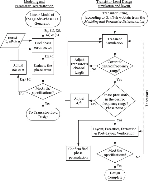
FIGURE 12.10 Design and verification flow: (a) modeling and parameter determination and (b) transistor-level design, simulation, and layout.
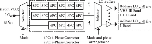
FIGURE 12.11 A direct injection-locked four-/eight-phase LOG.
Similarly to the ring oscillator, the robustness of the phase corrector can be improved by adopting a supply regulator and a bandgap reference to cope with the voltage and temperature variations, respectively. Simulations show that the regulator should stabilize the power supply with less than 80 mV fluctuation such that the phase noise of the multiphased LO will not be degraded by more than 1 dB at 1 MHz frequency offset. Those schemes are under development and have not been included in this work.
In the receiver measurements, the third- and fifth-order HR ratios are 35 and 39 dB, respectively, confirming the high phase precision of the LOG. Note that, to increase the accuracy, the data are averaged values of 12 samples with σ of 1.8 and 2.4 dB, respectively.
The phase noise performance of the LOG was characterized using a signal generator as LOin, as shown in Figure 12.12(a). The measured phase noise (Figure 12.12b) is well below that achieved in Vassilios et al. [17], which uses a practical PLL + VCO as LOin. Thus, the phase noise induced by the LOG should be tolerable when the PLL + VCO is presented.
The injection-locking characteristic of the LOG is of interest. When LOin is deactivated (Figure 12.13a), LOout is free running at its natural oscillation frequency of around 240 MHz and noticeable spurious tones appear throughout the spectrum. With LOin activated with a frequency of 205 MHz, LOout tracks LOin at the same frequency and the dynamic range is >60 dB (Figure 12.13b). On the other hand, the second to sixth harmonics will be suppressed by the differential I/Q mixer with HR. These results demonstrate that a high-purity multiphase LO can be achieved without frequency division.
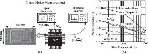
FIGURE 12.12 (a) Test setup for phase noise measurement and (b) measured phase noise of the LOG with one of the eight-phase outputs at 205 MHz.
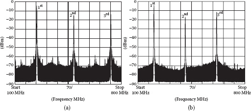
FIGURE 12.13 Measured injection-locking characteristic of the LOG: (a) free running at ~240 MHz; (b) injection locked at the desired 205 MHz.
Multiphase LO generators are critical blocks in modern wireless/wireline communication systems. This chapter has covered the design of an open-loop, inverter-only, four-/eight-phase LO generator. The corresponding mathematical models are developed so as to be easy to synthesize at a higher level, optimizing the device sizing with respect to phase error, power, and locking range. A four-/eight-phase LOG fabricated with a wireless receiver in 65 nm CMOS combines two chains of eight-phase correctors and one chain of four-phase corrector to cover the full-band mobile TV. Experimental results with the receiver prove that the third- and fifth-order HR ratios are 35 and 39 dB, respectively, confirming the high phase precision of the LOG, while adding relatively low phase error. The direct injection locking significantly reduces the spurious tones appearing throughout the spectrum.
1. D. Y. Jeong, S. H. Chai, W. C. Song, and G. H. Cho, CMOS current-controlled oscillators using multiple-feedback-loop ring architectures. IEEE International Solid-State Circuit Conference (ISSCC) Digest, pp. 386–387, 491, Feb. 1997.
2. J. Y. Chang, C. W. Fan, C. F. Liang, and S. I. Liu, A single-PLL UWB frequency synthesizer using multiphase coupled ring oscillator and current-reused multiplier. IEEE Transactions on Circuits and Systems—II: Express Briefs, vol. 56, no. 2, pp. 107–111, Feb. 2009.
3. L. C. Cho, C. Lee, and S. I. Liu, A 1.2 V 37–38.5 GHz eight-phase clock generator in 0.13 mm CMOS technology. IEEE Journal of Solid-State Circuits (JSSC), vol. 42, no. 6, pp. 1261–1270, June 2007.
4. A. Rofougaran, J. Rael, M. Rofougaran, and A. Abidi, A 900 MHz CMOS LC-oscillator with quadrature outputs. IEEE International Solid-State Circuit Conference (ISSCC) Digest, pp. 392–393, Feb. 1996.
5 X. Gao, E. A. M. Klumperink, and B. Nauta, Advantages of shift registers over DLLs for flexible low jitter multiphase clock generation. IEEE Transactions on Circuits and Systems—II: Express Briefs, vol. 55, no. 2, pp. 244–248, March 2009.
6. J. M. Chou, Y. T. Hsieh, and J. T. Wu, Phase averaging and interpolation using resistor strings or resistor rings for multi-phase clock generation. IEEE Transactions on Circuits and Systems—I: Regular Papers, vol. 53, no. 5, pp. 984–991, May 2006.
7. M. J. Gingell, Single-sideband modulation using asymmetric polyphase networks. Electronic Communications, vol. 48, pp. 21–25, 1977.
8. F. Behbahani, Y. Kishigami, J. Leete, and A. A. Abidi, CMOS mixers and polyphase filters for large image rejection. IEEE Journal of Solid-State Circuits (JSSC), vol. 36, no. 6, pp. 873–887, June 2001.
9. K. H. Kim, P. W. Coteus, D. Dreps, S. Kim, S. V. Rylov, and D. J. Friedman, A 2.6 mW 370 MHz to 2.5 GHz open-loop quadrature clock generator. IEEE International Solid-State Circuit Conference (ISSCC) Digest, pp. 458–627, Feb. 2008.
10. K. H Kim, D. M. Dreps, F. D. Ferraiolo, P. W. Coteus, S. Kim, S. V. Rylov, and D. J. Friedman, A 5.4 mW 0.0035 mm2 0.48 psrms-jitter 0.8 to 5 GHz non-PLL/DLL all-digital phase generator/rotator in 45 nm SOI CMOS. IEEE International Solid-State Circuit Conference (ISSCC) Digest, pp. 98–99, 99a, Feb. 2009.
11. K.-F. Un, P.-I. Mak, and R. P. Martins, An open-loop octave-phase local-oscillator generator with high-precision correlated phases for VHF/UHF mobile-TV tuners. Proceedings of IEEE International Symposium on Circuits and Systems (ISCAS), pp. 433–436, May 2009.
12. K.-F. Un, P.-I. Mak, and R. P. Martins, Analysis and design of open-loop multi-phase local-oscillator generator for wireless applications. IEEE Transactions on Circuits and Systems—I: Regular Papers, vol. 57, no. 5, pp. 970–981, May 2010.
13. A. Rezayee and K. Martin, A three-stage coupled ring oscillator with quadrature outputs. Proceedings IEEE International Symposium on Circuits and Systems (ISCAS), pp. 484–487, May 2001.
14. P. R. Gray and R. G. Meyer, Analysis and design of analog integrated circuits, 3rd. ed. New York: Wiley, 1993.
15. P.-I. Mak and R. P. Martins, A 0.46 mm2 4 dB NF unified receiver front-end for full-band mobile TV in 65 nm CMOS. IEEE Journal of Solid-State Circuits, pp. 1970–1984, Sept. 2011.
16. P.-I. Mak and R. P. Martins, A 0.46 mm2 4 dB NF unified receiver front-end for full-band mobile TV in 65 nm CMOS. IEEE International Solid-State Circuit Conference (ISSCC) Digest, pp. 172–173, Feb. 2011.
17. I. Vassilios, K. Vavelidis, N. Haralabidis, et al., A 65 nm CMOS multistandard, multiband TV tuner for mobile and multi-media applications. IEEE Journal Solid-State Circuits, vol. 43, pp. 1522–1533, July 2008.