
CONTENTS
14.2.1 Sensor Operation Principle and Oscillator-Based Frequency-Shift Detection
14.2.2 Sensor Signal-to-Noise Ratio Characterization
14.3 Sensor Design Scaling Law
14.4 A CMOS Implementation Example (System Architecture)
14.5 A CMOS Implementation Example (Circuit Blocks)
14.5.3 Multiplexers and Buffers
14.5.4 Divide-by-2 and Divide-by-3 Frequency Dividers
14.6.2 Magnetic Sensing Measurements
14.7 Discussion and Conclusion
Future point-of-care (PoC) molecular-level diagnostic systems require advanced bio-sensors that can offer high sensitivity, ultraportability, and a low price tag. Targeting on-site detection of biomolecules, such as DNAs, RNAs, or proteins, this type of system is believed to play a crucial role in a variety of emerging applications such as in-field medical diagnostics, epidemic disease control, and biohazard detection [1,2].
Conventionally, microarray technology is used to provide sensing information for biomolecules [3]. However, traditional microarray systems rely on optical detection setups for fluorescent molecular tags. This requires bulky and expensive optical devices including multiwavelength fluorescent microscopes, which limit the usage of optical microarray for PoC applications.
Another type of sensor modality, electrochemical biosensors, detects target molecules based on their extra electrical charges or dielectric properties. This includes detection schemes, such as impedance spectroscopy [4], amperometric analysis, redox cycling [5], and cyclic voltammetry [6]. However, electrochemical biosensors are subject to excessive noise at the electrode–electrolyte interface induced by drift and diffusion effects [7]. Moreover, this type of modality is sensitive to the offset and background perturbations, which are exacerbated by in-field measurement environments. These issues limit the typical detection sensitivity to several tens or hundreds of nanomolars [4–6]—orders of magnitude higher than the analyte concentrations in typical biochemical tests.
On the other hand, sensor platforms based on magnetic micro- or nanoparticle labels have been proposed as a promising biosensing scheme to augment or replace these sensing modalities for PoC applications. Affinity-based sandwich assays, such as enzyme-linked immunosorbent assay (ELISA) [8], are typically used in magnetic sensing processes (shown in Figure 14.1). The sensor surface is first coated with the desired molecular probes, which have high affinities with the target molecules. Then the test samples are introduced, and the target molecules are captured by the predeposited molecular probes through the surface chemistry. Finally, the surface-activated micro- or nanomagnetic labels are fed into the system and immobilized onto the sensor surface by the captured target molecules. Therefore, by detecting the existence of those magnetic labels, one can infer the presence of the target molecules in the incoming test sample.
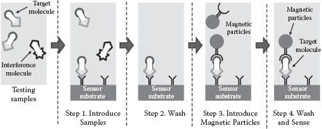
FIGURE 14.1 Typical sensing procedures of a magnetic biosensor using affinity-based sandwich assay.
In comparison to optical microarrays and electrochemical sensors, magnetic biosensors provide the following advantages: First, they directly eliminate bulky and expensive optical devices, making a low form factor and a low system cost possible. Second, magnetic labels do not have the signal quenching or decaying problems often encountered in fluorescence-based optical detection systems, making the magnetic sensing scheme more robust. Moreover, since most biosamples produce negligible magnetic signals compared to the magnetic labels, magnetic biosensing can achieve a very high signal-to-background-noise ratio. In addition, magnetic particle labels provide a powerful and versatile way of micromanipulation on both the cellular and molecular levels. This can be realized by designing and distributing the excitation electrical currents on-chip [9]; they create a magnetic field and apply forces on the nearby magnetic labels. Based on the high-integration level and the complex digital control capabilities supported in CMOS (complementary metal oxide semiconductor) processes, this on-chip magnetic manipulation concept can potentially be extended to a reconfigurable microfluidic platform particularly useful for tissue engineering.
Currently reported integrated magnetic sensor schemes include giant magneto-resistance (GMR) sensors [10–11,12], Hall effect sensors [13,14], and nuclear magnetic resonance (NMR) relaxometers [15]. However, these magnetic detection schemes require externally generated magnetic fields to bias the immobilized magnetic labels during their sensing processes. Moreover, expensive fabrication processes such as multilayer metal sputtering and deep dry etching on the passivation layers are demanded in those sensor fabrications. Consequently, these issues affect those systems’ ultimate form factors, total power consumption, and manufacturing cost.
To address these impediments, we propose an ultrasensitive frequency-shift-based magnetic biosensing scheme that is fully compatible with standard CMOS processes with no need for costly postprocessing steps or any electrical or permanent external biasing magnets [16]. The core of the sensor is an on-chip low noise LC oscillator, whose oscillation frequency will experience a downshift due to the presence of the magnetic labels on the sensor surface during the detection process. This sensor scheme is conducive to implementing a very large scale magnetic microarray without suffering from significant design complexity and manufacturing cost penalty. This can be achieved by integrating more sensor units onto a single chip and tiling the chips to form the entire sensor system [17]. Therefore, the proposed frequency-shift-based magnetic biosensing scheme presents itself as an ideal solution for PoC molecular-level diagnostic applications.
This book chapter is organized as follows. Section 14.2 focuses on the sensor mechanism. Theoretical modeling on the sensor transducer gain and the fundamental sensor noise floor is demonstrated to yield the sensor signal-to-noise ratio (SNR). The line-width narrowing effect is also presented to justify the advantage of oscillator-based frequency-shift detection. Section 14.3 demonstrates the design optimization to maximize the sensor SNR under various practical implementation constraints. As a design example, an eight-cell frequency-shift-based sensor array realized in a 130 nm CMOS process is demonstrated [18]. The system architecture and the key building blocks are covered in detail in Sections 14.4 and 14.5, respectively. Section 14.6 presents the measurement results of the sensor system for both electrical performance and magnetic sensing. To the authors’ best knowledge, this sensor example achieves the best sensitivity among the CMOS magnetic biosensors reported so far.
14.2.1 SENSOR OPERATION PRINCIPLE AND OSCILLATOR-BASED FREQUENCY-SHIFT DETECTION
The core of our proposed sensing scheme is an on-chip LC resonator (Figure 14.2). The current through the on-chip inductor generates a magnetic field and polarizes the magnetic particles present. This polarization leads to an increase of the total magnetic energy in space and thereby the effective inductance of the inductor. The corresponding resonant frequency downshift of the LC tank is given as
(14.1) |
where and are the nominal inductance and capacitance, while ΔL is the inductance increase due to the magnetic particles. Therefore, this downshift indicates the existence of the immobilized magnetic particles on the sensor surface, based on which one can infer the presence of the target molecules in the incoming test sample (Figure 14.1).
To detect this frequency downshift, one approach is to measure the LC resonator’s impedance in its amplitude and/or phase directly by precision circuits, such as a Wheatstone bridge. However, the line width of the tank impedance is fundamentally determined by its quality factor. For a standard CMOS process, this quality factor is often limited by the on-chip inductor quality factor Q (typically 10 to 20). In contrast, for an on-chip spiral sensing inductor with Dout of 100 ~ 200 μm, a single micron-size magnetic particle label typical only induces a part per million (ppm, i.e., 10–6) or even sub-ppm level relative frequency shift. Moreover, to provide a sensitive on-chip impedance measurement solution, the system requires fully integrated high-quality test tone generation, frequency sweeping, and analog-to-digital conversions, which add significantly to the design complexity.
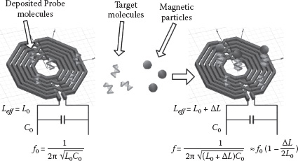
FIGURE 14.2 Proposed frequency-shift-based magnetic sensor scheme.
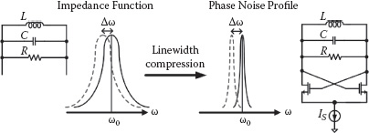
FIGURE 14.3 Line-width compression effect of oscillator phase noise profile compared with passive tank impedance function, assuming that the same LC tank is used.
On the other hand, if the same on-chip LC tank is implemented as an oscillator’s resonator, based on the virtual damping phenomena, the line width of the oscillator’s phase noise profile will experience a significant line-width compression effect compared with that of the LC tank impedance function (Figure 14.3) [19]. For a gigahertz range CMOS oscillator, this line-width compression ratio is typically between 10–8 and 10–9. Therefore, oscillator-based frequency detection provides an ultrasensitive measurement platform, which can be readily used to discern the sub-ppm level relative frequency shift in sensing the micron or nanometer size magnetic labels. In addition, a simple frequency counter can be implemented locally to the sensor oscillator and directly provides the digital measurement output of the oscillation frequency. Compared with the aforementioned impedance measurement approach, the oscillator-based frequency sensing provides a much more compact and simplified solution conducive to very large scale sensor array implementations with high pixel density.
14.2.2 SENSOR SIGNAL-to-NOISE RATIO CHARACTERIZATION
To characterize the proposed oscillator-based frequency-shift magnetic sensing platform fully, both its signal response (transducer gain) and the measurement noise floor will be discussed in this section. Subsequently, boldface letters denote vectors and italics denote scalars in the following context.
14.2.2.1 Sensor Transducer Gain
Most off-the-shelf magnetic particle labels are superparamagnetic; induced magnetization vector M under external polarization magnetic field H can be expressed by a Langevin function and further approximated at room temperature as
(14.3) |
where Msat is the saturation magnetization, μ0 is the magnetic permeability in vacuum, mp is the magnetization factor, and χe f f is the effective susceptibility of the superparamagnetic material [20]. The quantity k stands for the Boltzman constant and T for the temperature. Considering the demagnetization effect [21], based on the χe f f and the demagnetization factor D, the apparent magnetic susceptibility χapp of the label particles can be calculated; this characterizes how their magnetizations respond to the external polarization field. Since both D and χapp depend on the exact shape of the polarized magnetic objects, they are typically three-dimensional vectors even if the object is made of isotropic magnetic material. But, with a spherical shape assumption for the magnetic particles, both D and χapp can be simplified as scalar quantities [21].
Assume that the electrical current I conducting through the sensing inductor generates an excitation magnetic field of Hext. If there are N immobilized magnetic particles, each with an equal volume of Vm and located at ri = xi, yi, zi, i ∈ [1, N] in the vicinity of the sensor surface, the total magnetic energy increase in the space due to the particles’ magnetic polarizations by Hext is given by
(14.4) |
if the interactions among the adjacent magnetic particles are negligible and Hext(ri) can be treated as a uniform polarization field across the volume Vm for the ith magnetic particle. Therefore, the effective inductance change ΔL is given as
(14.5) |
where Bext2 is the spatially averaged excitation magnetic flux density for the N magnetic particles. Consequently, the averaged transducer gain can be defined as
(14.6) |
The preceding equation shows that the sensor signal is composed of three factors multiplied together. The first factor, χapp/2μ0, is related only to the magnetic property and the particle shape, while the last factor, Vm, is determined by the particle size. Both of them can be treated as constant values for a given type of magnetic label, assuming the local magnetic field strength does not saturate the particle’s magnetic susceptibility. However, the middle factor stands for an excitation magnetic field factor, which is proportional to the magnitude square of the polarization magnetic field per unit current and normalized by the sensing inductance value. Therefore, in order to achieve a large sensor transducer gain, the sensor inductor design should maximize the average excitation magnetic field strength per unit current and at the same time minimize its nominal inductance value.
In addition, the spatial “spot” sensor transducer gain at the location r = x, y, z is given as
(14.7) |
where Bextr is the excitation magnetic flux density at the location r.
14.2.2.2 Sensor Noise Modeling
Frequency counting can be used to determine the sensing oscillator’s frequency shift induced by the immobilized magnetic particle labels. During frequency counting, the total number of transitions M for the oscillator transient voltage waveform is measured within a given counting time window T. The measured frequency f is then given by
(14.8) |
The oscillator’s accumulated jitter within the window T presents transition errors of its waveform, which lead to total phase error ϕT and the frequency counting error Δ f as
(14.9) |
where Merr,T = ϕT/2π stands for the measurement uncertainty for the number of transitions within time T. Therefore, the noise floor for frequency counting can be formulated based on the sensing oscillator’s accumulated jitter σT2 within the counting window T as
(14.10) |
where Δf is the uncertainty in frequency and f 0 is the nominal frequency. In general, the window T is assumed to be derived from a stable off-chip frequency reference such as an oven-controlled crystal oscillator (OCXO), whose frequency uncertainty is negligible compared to that of the sensing oscillator.
Assuming that ϕt is the excessive noisy phase of the oscillator, the accumulated jitter σT2 is fundamentally determined by the sensing oscillator’s phase noise as
(14.11) |
where Sϕ,DSBω and Sϕ,DSBω are the double side band (DSB) and single side band (SSB) phase noise power spectrum densities, respectively [22]. The quantity ω is the phase noise offset frequency, and ω0 is the nominal oscillation frequency. In the following discussions, Sϕω will be used to denote the SSB phase noise Sϕ,SSBω. Therefore, based on (14.10) and (14.11), the relative frequency measurement error σΔf / f02 can be related to the phase noise as
(14.12) |
The phase noise Sϕω for a CMOS-based oscillator typically contains both 1/f and 1/f phase noise components. The former is due to up-conversion and folding of the thermal noise in the oscillator circuit, while the latter is caused by up-conversion of the flicker noise mainly from the oscillator’s active devices (Figure 14.4a). This frequency measurement uncertainty σΔf / f02 can be shown to be a function of the actual counting window T as follows.
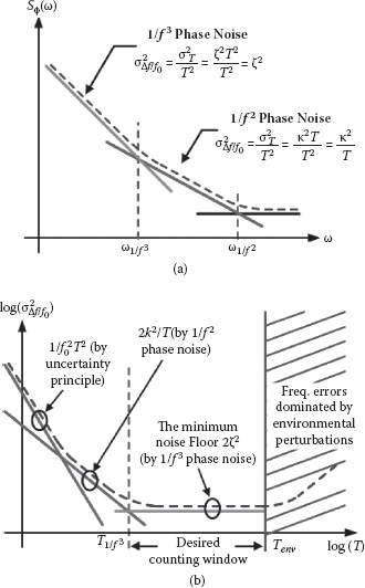
FIGURE 14.4 (a) Typical phase noise profile of an oscillator. (b) Frequency measurement uncertainty versus counting window T in differential operation. The curve is the overall frequency counting uncertainty for a given T with the minimum noise floor of 2.
For a small T—that is, T≪2π/ω1f3, where ω1f3 is the 1/ f corner frequency for the phase noise profile Sϕω—the jitter due to 1/ f phase noise dominates the relative frequency error σΔf / f02, which becomes inversely proportional to T as
(14.13) |
Here, k is the 1/ f jitter coefficient for the sensing oscillator [22]. Note that σΔf / f02 decreases when the window T is increased for a longer counting window. This is because the 1/ f phase noise behaves like white frequency noise [23], where the uncertainties in edge transition times are uncorrelated and, as a result, the accumulated jitter power σT2 is only linearly proportional to T, shown in (14.13). Thus, the frequency measurement error σΔf / f02 due to the 1/ f phase noise, as its normalized accumulated jitter (14.12), can always be reduced using a longer counting time window T.
However, when T is large enough (T>>2π/ω1f3), phase noise dominates and results in the frequency error σΔf / f02 actually independent of T as
(14.14) |
where ζ is the 1/ f jitter coefficient for the sensing oscillator [22]. This is due to the fact that 1/ f phase noise is flicker frequency noise [23], whose edge transition uncertainties are strongly correlated, leading to σT2 being proportional to T2 (14.14). Since σΔf / f02 is independent of the window length T for this case, this ζ2 factor therefore determines the fundamental noise floor for the oscillator-based frequency measurement.
In addition, a measurement error proportional to 1/ fT due to the uncertainty principle should be superimposed onto the aforementioned two frequency errors. This 1/ fT error suggests that a frequency resolution of 1 Hz can only be achieved with a counting window longer than 1 second. The total measurement noise with respect to window T is plotted and reveals that the 1/ f phase noise (ζ2) indeed determines the ultimate sensor noise floor (Figure 14.4b).
In practical implementations, differential sensing can be used to further reject the environmental perturbations, such as temperature drifting and supply variations. This scheme can be implemented as two identical oscillators—one used for sensing and one used as a reference both physically placed close to each other and sharing the same electrical supply and biasing circuits (shown as an example later in Figure 14.7). Therefore, the environmental variations present themselves as common-mode perturbations to the two oscillators and can be readily suppressed by differential operations (i.e., taking the frequency difference of the sensing and reference oscillators as the sensor output). Note that in this case, since the phase noise is uncor-related between the two oscillators, the total noise power after the differential sensing actually doubles, if the two oscillators are assumed to have the same phase noise power spectrum density (PSD) (Figure 14.4b). The extra factor of two accounts for the noise power doubling.
Therefore, the overall sensor SNR in the differential sensing scheme can be formulated as
(14.15) |
where the frequency shift Δf f 0 and error 2σΔf / f0 for a given sensing oscillator and magnetic particle distribution can be calculated based on (14.6) and (14.12), respectively. The factor of two is to account for the noise power doubling due to differential sensing.
14.3 SENSOR DESIGN SCALING LAW
The theoretically derived SNR expression enables sensor design optimization, which will be discussed in detail in this section.
First, for the sensor signal response, the transducer gain equation (14.6) demonstrates that for a given type of magnetic particle label, the factors related to the magnetic material and the particle volume are both constants. The field factor Bext2I2L, determined by the sensing inductor geometry, is therefore the only factor subjected to design optimization.
The effect of the sensor noise floor σΔf / f02 with respect to the sensing inductor design (inductance L and quality factor Q) is discussed next. Since the fundamental noise floor is determined by the 1/f 3 phase noise, only flicker noise will be considered for the following derivation.
For a given process technology, assuming a fixed biasing current density for the oscillator active-core devices and a constant tank amplitude (limited by the supply VDD), the transistors’ DC biasing current and width W are related to the tank inductor design as
(14.16) |
where Rtank is the tank’s parallel resistance and Q is its quality factor of the tank (typically dominant by the tank inductance Q in CMOS processes), both at the resonant frequency ω0. The result of Id ∝ VDD/Rtank assumes that the oscillator is biased for its optimum operation (i.e., the boundary region between the current-limiting and voltage-limiting regime) [22]. Moreover, for a fixed biasing current density, the device DC current is proportional to its drain output flicker current noise PSD, 1/f2ω = β/ω, as
(14.17) |
The 1/f 3 jitter coefficient ζ can be derived using the linear time-varying (LTV) phase noise model at a given offset frequency ω [22], and further simplified based on (14.16) and (14.17) to
(14.18) |
where A0 is the DC term of the oscillator’s impulse sensitivity function (ISF) Γ(t) and qmax is the tank maximum charge swing [22]. Therefore, assuming differential operation, the relationship between the sensor noise power σΔf / f02 and the inductor L and Q is given by
(14.19) |
This result suggests that the sensor noise floor also depends on the sensor inductor design. Consequently, based on (14.6) and (14.19), the averaged sensor SNR of a single magnetic particle can be obtained as
(14.20) |
This equation shows that the sensor inductor design is the key to optimizing the magnetic sensor performance and maximizing its SNR during magnetic sensing.
As an example, the normalized averaged SNR for a six-turn symmetric inductor detecting a single magnetic bead (D = 1 μm) at 1 GHz is shown in Figure 14.5. In this example, both the outer diameter (D) and the inductor trace width are swept while the trace separation is kept constant at 3.5 μm. For a given D, the SNR does not vary significantly with the width. This is because, for a constant D, both the inductance L and the averaged Bext2/I2 scale the same with the inductor width. This leads to a relatively constant SNR for a given outer diameter.
On the other hand, for the same trace width, a smaller D gives a much higher averaged SNR. This is due to a larger Bext2/I2 (i.e., a more concentrated excitation magnetic field) and a smaller inductance value at a smaller inductor footprint (i.e., a smaller D). However, an inductor with an exceedingly small size is practically undesirable for several reasons. First, the LC tank’s metal interconnections start to contribute non-negligible resistances and parasitic inductances comparable to the sensor inductance, which degrades the sensor SNR by lowering both Q and ΔLL0 during sensing. Moreover, to maintain the same voltage amplitude at the operating frequency, a low impedance tank (for a small L) needs to conduct a larger current, which is susceptible to causing magnetic saturation of the particles and yields the decreased detected magnetic signal due to susceptibility χapp degradation as mentioned previously. Furthermore, the frequency-dependent magnetic loss, which degrades the magnetic signal, limits the maximum operation frequency to around 1 GHz for magnetic beads formed by nanometer size magnetic particles suspended in nonmagnetic structures [25,26]. Thus, the inductor size cannot be too small in order to achieve an acceptable Q at the desired operation frequency. In addition, the design space for the sensing inductor is also limited by other constraints, such as the sensor pixel size (footprint) and power consumption.
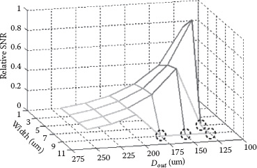
FIGURE 14.5 The simulated averaged SNR for a six-turn differential symmetric inductor with different geometric sizes at 1 GHz operating frequency. The dotted circles indicate inductor geometries unrealizable due to layout rules.
14.4 A CMOS IMPLEMENTATION EXAMPLE (SYSTEM ARCHITECTURE)
In this section, an eight-cell sensor array implemented in a standard 130 nm CMOS process will be demonstrated as a design example for the proposed frequency-shift magnetic sensing scheme. The system architecture is shown in Figure 14.6.
The differential sensing scheme is implemented for each sensor cell. It is composed of two well matched sensor oscillators for sensing and reference operations, both operating at a nominal frequency of 1 GHz (Figure 14.7). In the layout, the active cores of the two oscillators are placed in proximity to improve matching and to minimize local temperature differences. The oscillator pair also shares the same power supply, biasing, and ground lines. As discussed before, these implementation techniques ensure that the environmentally related low frequency noise and drifting appear as the common-mode perturbations and are subsequently suppressed by the differential operation. The active and the reference oscillators are turned on alternately in time to avoid parasitic injection locking or oscillator pulling.
On-chip temperature controllers are implemented in this design. They regulate the local temperature for the oscillator active cores through a thermal-electrical feedback loop. This further reduces frequency drifting induced by ambient temperature changes. Instead of regulating the entire chip, the temperature controllers are placed locally at every sensor cell, regulating the differential sensing oscillators’ active core temperature to achieve more efficient thermal control with minimal power consumption overhead.
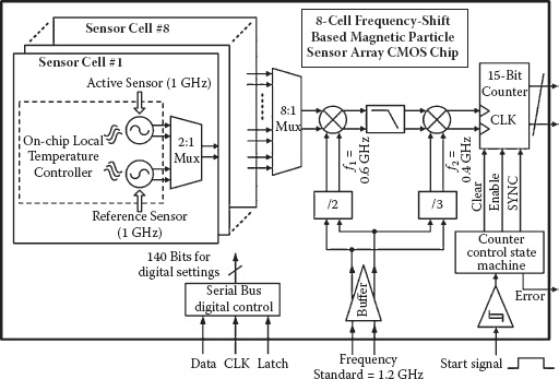
FIGURE 14.6 The eight-cell frequency-shift-based CMOS magnetic biosensor array system architecture.
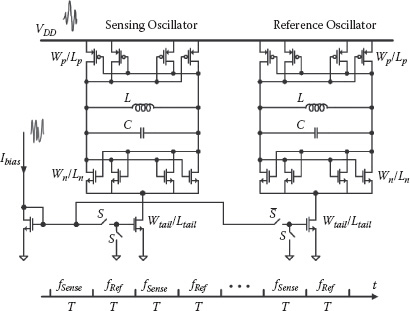
FIGURE 14.7 Schematic of the differential sensing oscillators. The two sensor oscillators are alternatively turned on to perform differential sensing schemes.
Frequency counters are used to detect the sensing signal’s frequency shift and provide direct digital output. To facilitate resolving a ppm or sub-ppm level frequency shift at 1 GHz, a two-step down-conversion architecture is used to shift the 1 GHz sensor output to a tunable kilohertz range baseband frequency. Unlike direct down-conversion, this architecture guarantees that the two LO signals (0.6 and 0.4 GHz) are not close to the sensor free-running frequency or its dominant harmonics and, hence, inherently prevents pulling or injection locking on the sensing oscillator pair. By using a 15-bit baseband frequency counter, a maximum counting resolution of better than 3 × 10⁻⁴ ppm (0.3 Hz at 1 GHz) can be achieved. Note that digital nature of the sensor system’s output signal facilitates tiling multiple sensor array chips to form a very large scale magnetic microarray for high throughput applications.
14.5 A CMOS IMPLEMENTATION EXAMPLE (CIRCUIT BLOCKS)
In this section, circuit designs for the major building blocks in the example sensor array system are presented in detail.
A differential complementary cross-coupled topology is used for the sensing oscillator, as shown in Figure 14.7. Switches at the tail current sources control the turning on and off of the oscillators, whose bias current is derived from the same master current source. Common centroid layout is used to improve matching and design robustness against process gradients. Since the 1/f 3 phase noise determines the ultimate noise floor of the sensor, a gate length of 240 μm is used for both the negative (N) MOS and positive (P)MOS transistors in the cross-coupled pair to lower the device flicker noise corner. Moreover, the relative weighting between the NMOS active pair and the PMOS active pair is optimized to shape the oscillation transient voltage waveform and minimize the flicker noise up-conversion from the NMOS current tail [27]. Furthermore, to provide frequency tuneability of the sensing oscillator, a switched capacitor bank has been adopted to set the desired operating frequency.
Based on the noise analysis described in Section 14.2.2.2, a design goal for the 1/f 3 phase noise of the sensor oscillator can be obtained, which achieves a given frequency-shift detection sensitivity. For the differential sensing scheme, the frequency counting noise floor σΔf / f0, di f f has been shown to be 2ζ, with ζ as the 1/f 3 jitter coefficient of the oscillator. Numerically, this ζ factor can be obtained from the oscillator’s SSB 1/f 3 phase noise profile, Sϕω = c/ω3, based on a close-in corner frequency approximation in Liu and McNeil [24] as
(14.21) |
Therefore, in order to achieve a frequency-shift noise floor of less than 1 ppm in a differential operation, the SSB 1/f 3 phase noise for the sensing oscillator should be below –43.9 dBc/Hz at a 1 kHz frequency offset for a center tone of 1 GHz. For a 0.1 ppm frequency resolution, the phase noise at an offset of 1 kHz should be –63.9 dBc/Hz.
On-chip temperature regulators are implemented locally for each individual differential sensing cell. A temperature controlling system is typically composed of an electrical-thermal feedback loop. This loop senses the difference between the on-chip and the target temperature and converts it to an electrical signal, which drives an on-chip heater for thermal controlling.
The simplified schematic of our temperature regulator is shown in Figure 14.8. The temperature sensor is implemented as a PTAT (proportional to absolute temperature) voltage, and a bandgap voltage is used as the temperature reference. The PTAT voltage is programmable with 12-bit control on its output resistors; this sets the target temperature for thermal regulation. The voltage difference between the two temperature signals is then amplified by a two-stage buffer to drive a heater transistor array. A feedback op-amp is used to lock the common-mode output voltage of the driver to the threshold voltage of a dummy heater transistor. This provides a reliable stand-by driver output voltage to prevent any false turning on of the heater transistors due to process variations or modeling inaccuracy. The thermal response of the heater array is simulated using Ansoft® Ephysics [28]. Overall, this thermal controller forms a first-order electrical-thermal feedback loop with a typical DC loop gain of 20.5 dB and is stabilized by a dominant pole in the kilohertz range.
The layout configuration of the temperature regulator is shown in Figure 14.9. The bandgap core, including the reference and the PTAT generation, is placed close to the two oscillators’ active devices for accurate temperature sensing. The heater array, composed of power PMOS transistors, forms a ring structure surrounding the oscillator active cores to minimize the spatial temperature difference within the regulator.
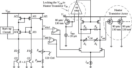
FIGURE 14.8 Simplified schematic for the on-chip temperature regulator.
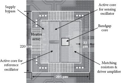
FIGURE 14.9 The layout configuration of the heater structure for one differential sensing cell.
14.5.3 MULTIPLEXERS AND BUFFERS
Multiplexers and buffer amplifiers together with distribution lines deliver the output signals from the selected sensor cells to a down-conversion block (Figure 14.10). Resistive degeneration is used to linearize the distribution circuit gain. To ensure an adequate bandwidth without peaking inductors or excessive power consumption, signals are distributed in current mode through a modified cascode topology [29]. The low impedance at the current summing nodes minimizes the bandwidth penalty due to parasitic capacitances. Since only buffers for the selected branch need to be turned on at any given time, the distribution system overall consumes 10 mA from a 2.5 V supply and has a –3 dB bandwidth of 2.5 GHz.
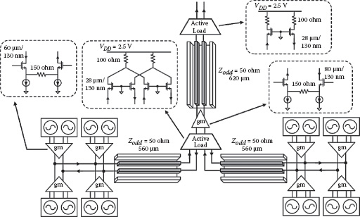
FIGURE 14.10 Schematic for the signal distribution network.
14.5.4 DIVIDE-BY-2 AND DIVIDE-BY-3 FREQUENCY DIVIDERS
To synthesize the down-conversion LO signals, static divide-by-2 and divide-by-3 circuits are implemented in current mode logic (CML) as high-speed digital dividers. Both dividers are composed of feedback D-flip-flops (Figure 14.11) and provide divided signals with a 50% duty cycle to suppress unwanted harmonics. With these dividers, an off-chip 1.2 GHz frequency reference signal is divided into 600 and 400 MHz LO signals that down-convert the sensor oscillators’ nominal 1 GHz signal. This frequency plan ensures that both LO signals are separated from the fundamental tone and the dominant harmonics of the sensor free-running frequency to prevent oscillator pulling or injection locking on the sensing oscillator pair. Note that although the 1.2 GHz reference signal is fed from off-chip in this implementation, it can also be synthesized on-chip and locked to a megahertz crystal frequency standard. In this case, the presented down-conversion frequency plan also ensures that this 1.2 GHz tone is away from the 1 GHz sensor oscillators. The dividers consume 8 mA from a 1.2 V supply and add negligible noise to the 1.2 GHz reference signal.
The chip microphotograph for the example eight-cell magnetic sensor array is shown in Figure 14.12. The entire chip is implemented in a standard 130 nm 1P8M CMOS process and occupies an area of 3.0 × 5.2 mm2. All the critical building blocks are highlighted. Note that the bonding pads are placed along the upper chip edge. This configuration accommodates the integration of the PDMS (polydimethylsiloxan) microfluidic structures for biosample delivery without perturbing the wire bonds. The wire bonds can be eventually sealed and protected by the PDMS solution [30]. A minimum distance of 250 μm between adjacent sensing inductors is used, limited by the minimum achievable microfluidic channel width/separation in our in-house PDMS fabrication facilities. This spacing between sensor cells can be substantially reduced by employing more advanced microfluidic processes. The CMOS sensor chip integrated with the PDMS structure is shown in Figure 14.13.
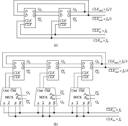
FIGURE 14.11 Schematic for the frequency dividers with 50% duty cycle: (a) divide-by-2; (b) divide-by-3.
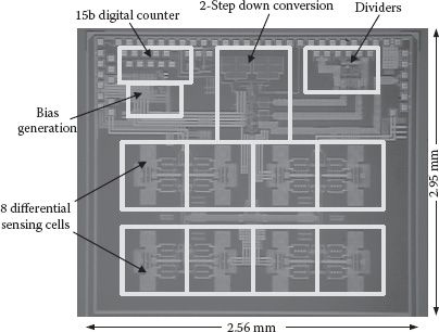
FIGURE 14.12 Chip microphotograph of the CMOS sensor array.
In this section, the electrical performance of the sensor array is first presented. Magnetic sensing measurements are then shown for detecting micron size magnetic particles. The results demonstrate the full functionality of our proposed frequency-shift-based magnetic sensing scheme.
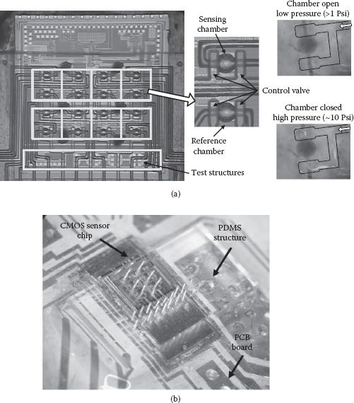
FIGURE 14.13 (a) Chip microphotograph of the CMOS sensor array with PDMS microfluidic structure. (b) Integration of the CMOS sensor chip, PDMS structure, and PCB board for the testing module.
The measured phase noise performance of the sensing oscillator is shown in Figure 14.14. Consuming 4 mA from a 1.2 V supply, the oscillator has its 1/f 3 phase noise (at 1 kHz frequency offset) from –59 to –61.8 dBc/Hz for different biasing scenarios with a center tone of 1.04 GHz. Based on the theoretical analysis, this phase noise level provides a frequency measurement uncertainty σΔf / f0 between 170.6 and 123.6 ppb (parts per billion, i.e., 10–9) in the differential operation scheme, which achieves a sub-ppm sensor sensitivity using frequency-shift detections.
The rejection of environmentally related drifting through differential counting is demonstrated in Figure 14.15. The frequency counting results for the sensor and reference oscillators are shown with and without differential operation. A slowly varying common-mode drift of the oscillation frequencies can be observed and is greatly suppressed by the differential operation. Consequently, in the differential operation mode, the measured relative frequency uncertainty σΔf / f0 is 130 ppb before averaging, which stays within the theoretical calculated noise range based on the phase noise measurement.
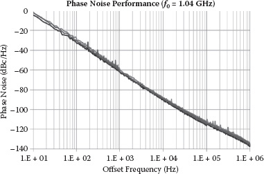
FIGURE 14.14 Measured and simulated phase noise performance of single sensing oscillator at different biasings.
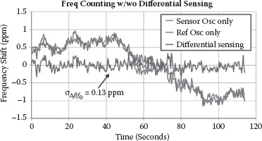
FIGURE 14.15 Suppression of common-mode frequency drifting through differential sensing.
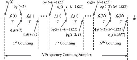
FIGURE 14.16 N-sample averaging on differential frequency counting measurements.
Moreover, the differential frequency counting samples can be averaged to improve the sensor SNR further (Figure 14.16). Let fSi and fRi stand for the frequency measurement in the ith differential counting interval. The total N-sample averaged differential frequency result is
(14.22) |
Therefore, using the preceding noise model and assuming that the sensor and reference oscillators present the same, yet uncorrelated power spectrum density, the frequency measurement noise power after averaging N differential samples can be formulated as
(14.23) |
where ϕS and ϕR are the excessive noisy phases for the sensor and reference oscillators, which are uncorrelated to each other. The ratio between the noise power of the N-sample-averaged differential frequency counting result over the unaveraged one can be defined as a noise power reduction ratio NPRR. The simulated NPRR with respect to the averaging sample number N is plotted in Figure 14.17. Note that the noise power for the N-sample averaging is not inversely proportional to the sample number N as the classical averaging scenario for sampled white noise (uncorrelated samples). This is because the waveform transition uncertainties due to 1/f 3 jitter in the frequency measurement exhibit strong correlations, resulting in a much lower suppression after averaging.
The thermal regulator response is depicted in Figure 14.18 as the total heater current versus on-chip temperature variations. The on-chip temperature is measured through the PTAT voltage. When the temperature deviates from the target setting (i.e., 29°C in this measurement), the PMOS heater ring starts to draw a DC current from the supply and heat up the enclosed differential sensing oscillators’ active cores. The measured heater responses for three different loop-gain settings are shown, closely matching the simulated responses.
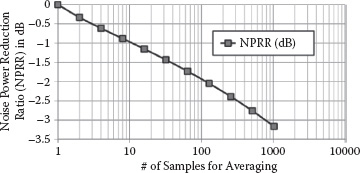
FIGURE 14.17 Simulated noise power reduction ratio, NPRR(N), based on sample averaging, when the phase noise is the dominant noise for the sensing oscillators. The x-axis stands for the number of differential frequency counting measurements.
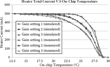
FIGURE 14.18 Simulated and measured heater total current versus on-chip temperature when the target temperature is set at 29°C.
TABLE 14.1
Measured Electrical Performance of the Sensor Array
Power consumption |
|
Sensor oscillatora |
4.0 mA at 1.2 V |
Down-conversion chain, multiplexera and counter |
39.6 mA at 2.5 V |
24. 3 mA at 2.5 V |
|
Total power consumption |
165 mW |
Thermal loop gain (nominal setting) |
20 dB |
Number of differential sensing cells |
8 |
Technology |
130 nm CMOS |
Chip area |
2.95 mm × 2.56 mm |
Sensor inductor size (Dout) |
140 μm |
a At any given time, only one sensor oscillator with its temperature controller and buffer will be turned on to avoid pulling and/or injection locking between oscillators.
b Here the target chip temperature is set at 29°C with the ambient temperature of 27°C. The 20 dB loop gain ensures the actual on-chip temperature is at 28.8°C.
The electrical performance of the example CMOS sensor array is summarized in Table 14.1
14.6.2 MAGNETIC SENSING MEASUREMENTS
To characterize the sensor’s magnetic sensing functionalities, two sets of experiments are performed on detecting three types of micron size magnetic particles (i.e., Dynabeads® M-450 Epoxy, Dynabeads® Protein G, and Dynabeads® MyOne™ [31]). The first set of experiments is used to verify the sensor’s capability of detecting a single, micron size magnetic particle. The second one is used to characterize the sensor’s dynamic range with a wide range of magnetic particle numbers.
In the first experiment, a single magnetic particle is introduced onto the sensor surface for all three bead types. The measurement results are summarized in Table 14.2. The frequency counting window is 0.1 s, and averaging on the sensing data is performed to improve the SNR further. With 160 s used for averaging, an SNR of 8.0 dB is achieved for detecting a single 1 μm magnetic particle (Dynabeads MyOne). After 90 s of averaging, the achieved SNRs for a single 2.4 and 4.5 μm magnetic particle (Dynabeads Protein G or Dynabeads M-450 Epoxy) are 28.6 and 40.0 dB, respectively. As a control sample, polystyrene beads (D = 1 μm) are tested. Polystyrene is the nonmagnetic structure material used to hold the nanomagnetic grains and form most off-the-shelf micron size magnetic bead products. The polystyrene beads show significantly lower frequency-shift responses compared with the 1 μm magnetic beads. This verifies that our sensor’s frequency shifts for the presented magnetic beads are mainly due to the inductance (magnetic) rather than the capacitance (dielectric) changes. Typical measurement results for a single magnetic bead of 2.4 and 1 μm are shown in Figure 14.19. The blue curves represent the data traces with cumulative averaging.
TABLE 14.2
Typical Sensor Response to Off-the-Shelf Magnetic Bead
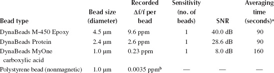
a The counting window T is 0.1 s for these measurements.
b This Af/f per bead is a calculated average value for a measured frequency shift of 100 polystyrene beads sensed at the same time.
In the second experiment, different numbers of magnetic beads for all three bead types are separately applied onto the sensor surface, and their corresponding frequency shifts are recorded respectively. Since the excitation magnetic field amplitude Bext(r) is generally not a constant across the sensor surface for a six-turn symmetric sensing inductor layout, the local transducer gain will consequently be spatially nonuniform based on (14.7). Therefore, in this experiment the distribution of the beads is first recorded by a high-magnification camera. Then their measured frequency shifts are normalized by their corresponding spatially averaged transducer gain factors, which are obtained through theoretical calculations based on the transducer gain model in (14.7). Note that the normalized frequency-shift results assume that all the beads’ responses are normalized to the center of the sensing inductor. The normalized and raw frequency-shift results versus bead numbers are plotted in Figure 14.20. The total bead count is limited to around 200 ~ 400 because, beyond this number, the beads start to aggregate on the sensor surface, which significantly prevents accurate bead identifications under the microscope. Nevertheless, the linear sensor responses after normalization prove the validity of our spatial sensor transducer gain modeling in (14.6) and (14.7). Moreover, this measurement demonstrates a sensor dynamic range of greater than 81 dB.
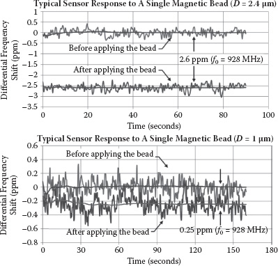
FIGURE 14.19 Typical sensor response of a single Dynabeads protein G (D = 2.4 mm) and MyOne (D = 1 mm).
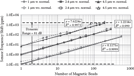
FIGURE 14.20 Measured sensor response with and without spatial transducer gain normalization. The counting window T is 0.1 s.
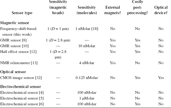
A sensor performance comparison among state-of-the-art CMOS-based biosensors is summarized in Table 14.3. Sensor testing results based on actual DNA samples are reported in Wang et al. [18]. The frequency-shift magnetic sensor array example presents the best sensitivity among the reported magnetic biosensors in CMOS and achieves a competitive performance compared to the reported CMOS biosensors.
14.7 DISCUSSION AND CONCLUSION
As an extension to the presented oscillator-based magnetic sensor array, a correlated double counting (CDC) frequency-shift sensor scheme is introduced in Wang, Hajimiri, and Kosai [33] and Wang et al. [34] to further decrease the minimum sensor noise floor below 2δ2 for the basic differential sensing case shown in (14.20). Through oscillator active core sharing, this scheme physically establishes 1/f 3 phase noise correlation between the sensing and the reference oscillators. Similarly to the common-mode environmental noise for the oscillator pair, the correlated 1/f 3 phase noise is then largely suppressed via subsequent differential sensing. This significantly reduces the overall sensor noise for the frequency-shift measurements without requiring either low 1/f 3 phase noise or power overhead. Moreover, averaging the CDC frequency counting data can be shown to present a much more effective noise suppression effect—that is, a lower NPRR(N)—compared to a standard differential scheme shown in (14.19), which further boosts the sensor SNR.
TABLE 14.3
Performance Comparison with Published CMOS Biosensors
In parallel, the issue of transducer gain uniformity is addressed in Wang and Hajimiri [35] and Wang, Sideris, and Hajimiri [36]. In this study, a two-layer stacked coil is proposed as the sensing inductor; this provides an equalized excitation magnetic field (in magnitude) across the sensor surface. In addition, floating shimming metal pieces are introduced to enhance the transducer spatial gain uniformity further. Therefore, the frequency-shift magnetic sensor achieves a linear sensor response versus the particle numbers without any postnormalization steps.
In summary, a novel frequency-shift-based magnetic biosensing scheme is introduced for future point-of-care (PoC) molecular diagnosis applications. Fully compatible with standard CMOS processes, the sensor scheme achieves high sensitivity, handheld portability, and low power consumption without using any external magnetic biasing fields or expensive postprocessing steps. Theoretical limits on sensor SNR and design optimization techniques have been presented. An eight-cell sensor array implemented in a standard 130 nm CMOS process has been demonstrated as a design example. Both electrical and magnetic sensing measurement results have been presented to verify the sensing scheme’s functionality. To the authors’ best knowledge, this presented magnetic sensor array example achieves the best sensitivity among the CMOS magnetic sensors reported so far.
The authors acknowledge Dr. Yan Chen, Dr. David Wu, and Mr. Constantine Sideris for their technical support during the sensor testing. The authors would also like to thank Professor Axel Scherer, Sander Weinreb, Azita Emami, and the members of the Caltech High-Speed Integrated Circuit (CHIC) Group for their helpful discussions.
1. N. K. Tran and G. J. Kost, Worldwide point-of-care testing: Compendiums of POCT for mobile, emergency, critical, and primary care and of infectious diseases tests. Journal Near-Patient Testing & Technology, vol. 5, no. 2, pp. 84–92, June 2006.
2. G. J. Kost, Principles and practice of point-of-care testing. Philadelphia: Lippincott Williams & Wilkins, 2002.
3. D. Stekel, Microarray bioinformatics. Cambridge, UK: Cambridge University Press, 2003.
4. A. Hassibi and T. H. Lee, A programmable 0.18 μm CMOS electrochemical sensor microarray for biomolecular detection. IEEE Sensors Journal, vol. 6, no. 6, pp. 1380–1388, Dec. 2006.
5. M. Schienle, C. Paulus, A. Frey, F. Hofmann, B. Holzapfl, P. Schinder-Bauer, and R. Thewes, A fully electronic DNA Sensor with 128 positions and in-pixel A/D conversion. IEEE Journal Solid-State Circuits, vol. 39, no. 12, pp. 2438–2445, Dec. 2004.
6. F. Heer, M. Keller, G. Yu, J. Janata, M. Josowicz, and A. Hierlemann, CMOS electro-chemical DNA-detection array with on-chip ADC. IEEE ISSCC Digest Technical Papers, pp. 168–169, Feb. 2008.
7. A. Hassibi, R. Navid, R. W. Dutton, and T. H. Lee, Comprehensive study of noise processes in electrode electrolyte interfaces. Journal Applied Physics, vol. 96, no. 2, pp. 1074–1082, July 2004.
8. B. Alberts, D. Bray, K. Hopkin, A. Johnson, J. Lewis, M. Raff, K. Roberts, and P. Walter, Essential cell biology, 2nd ed. New York: Garland Science/Taylor & Francis Group, 2003.
9. H. Lee, Y. Liu, D. Ham, and R. M. Westervelt, Integrated cell manipulation system—CMOS/microfluidic hybrid. Lab on a Chip, vol. 7, no. 3, pp. 331–337, March 2007.
10. G. Li, V. Joshi, R. L. White, S. X. Wang, J. T. Kemp, C. Webb, R. W. Davis, and S. Sun, Detection of single micron-sized magnetic bead and magnetic nanoparticles using spin valve sensors for biological applications. Journal Applied Physics, vol. 93, no. 10, pp. 7557–7559, May. 2003.
11. G. Li, S. Sun, R. Wilson, R. White, N. Pourmand, and S. X. Wang, Spin valve sensors for ultrasensitive detection of superparamagnetic nanoparticles for biological applications. IEEE Journal Sensors and Actuators A, vol. 126, pp. 98–106, Nov. 2006.
12. S. Han, H. Yu, B. Murmann, N. Pourmand, and S. X. Wang, A high-density magnetoresistive biosensor array with drift-compensation mechanism. IEEE ISSCC Digest Technical Papers, pp. 168–169, Feb. 2007.
13. T. Aytur, P. R. Beatty, and B. Boser, An immunoassay platform based on CMOS Hall sensors. Solid-State Sensor, Actuator and Microsystems Workshop, Hilton Head Island, SC, pp. 126–129, June 2002.
14. P. Besse, G. Boero, M. Demierre, V. Pott, and R. Popovic, Detection of a single magnetic microbead using a miniaturized silicon Hall sensor. Applied Physics Letters, vol. 80, no. 22, pp. 4199–4201, June 2002.
15. Y. Liu, N. Sun, H. Lee, R. Weissleder, and D. Ham, CMOS mini nuclear magnetic resonance system and its application for biomolecular sensing. IEEE ISSCC Digest Technical Papers, pp. 140–141, Feb. 2008.
16. H. Wang, A. Hajimiri, and Y. Chen, Effective-inductance-change based magnetic particle sensing. US Patent no. 20090267596 A1, March 7, 2008.
17. H. Wang and A. Hajimiri, Ultrasensitive magnetic particle sensor system. US Provisional Patent CIT-5224-P, Sept. 15, 2008.
18. H. Wang, Y. Chen, A. Hassibi, A. Scherer, and A. Hajimiri, A frequency-shift CMOS magnetic biosensor array with single-bead sensitivity and no external magnet. IEEE ISSCC Digest Technical Papers, pp. 438–439, Feb. 2009.
19. D. Ham and A. Hajimiri, Virtual damping and Einstein relation in oscillators. IEEE Journal Solid-State Circuits, vol. 38, no. 3, pp. 407–418, March 2003.
20. K. H. J. Buschow and F. R. de Boer, Physics of magnetism and magnetic materials. New York: Springer, 2003.
21. D. E. Bray and R. K. Stanley, Nondestructive evaluation. New York: Taylor & Francis Group, 1997.
22. A. Hajimiri and T. H. Lee, The design of low noise oscillators. New York: Springer, 1999.
23. D. A. Howe, D. W. Allan, and J. A. Barnes, Properties of signal sources and measurement methods. Proceedings of the 35th Annual Symposium on Frequency Control, 1981.
24. C. Liu and J. A. McNeil, Jitter in oscillators with 1/f noise sources. IEEE ISCAS Digest Technical Papers, pp. 773–776, May 2004.
25. P. Talbot, A. M. Konn, and C. Brosseau, Electromagnetic characterization of fine-scale particulate composite materials. Journal of Magnetism and Magnetic Materials, vol. 249, pp. 481–485, 2002.
26. C. Brosseau, J. B. Youssef, P. Talbot, and A. M. Konn, Electromagnetic and magnetic properties of multicomponent metal oxides heterostructures: Nanometer versus micrometer-sized particles. Journal of Applied Physics, vol. 93, no. 11, pp. 9243–9256, June 2003.
27. A. Hajimiri and T. H. Lee, Design issues in CMOS differential LC oscillators. IEEE Journal Solid-State Circuits, vol. 34, no. 5, pp. 717–724, May 1999.
29. A. Babakhani, X. Guan, A. Komijani, A. Natarajan, and A. Hajimjri, A 77-GHz phased-array transceiver with on-chip antennas in silicon: Receiver and antennas. IEEE Journal Solid-State Circuits, vol. 41, no. 12, pp. 2795–2806, Dec. 2006.
30. H. Wang and A. Hajimiri, Low cost bounding technique for integrated circuit chips and PDMS devices. US Provisional Patent CIT-5320-P, Feb. 25, 2009.
32. B. Jang, P. Cao, A. Chevalier, A. Ellington, and A. Hassibi, A CMOS fluorescent-based biosensor microarray. IEEE ISSCC Digest Technical Papers, pp. 436–437, Feb. 2009.
33. H. Wang, A. Hajimiri, and S. Kosai, Noise suppression techniques in high-precision long-term frequency/timing measurements. US Provisional Patent CIT-5318-P, Feb. 20, 2009.
34. H. Wang, S. Kosai, C. Sideris, and A. Hajimiri, An ultrasensitive CMOS magnetic bio-sensor array with correlated double counting (CDC) noise suppression. IEEE MTT-S International Microwave Symposium (IMS), May 2010.
35. H. Wang and A. Hajimiri, Effective-inductance-change magnetic sensor with spatially uniform transducer gain. US Provisional Patent CIT-5108-P, March 7, 2008.
36. H. Wang, C. Sideris, and A. Hajimiri, A frequency-shift based CMOS magnetic biosensor with spatially uniform sensor transducer gain. IEEE CICC Digest Technical Papers, pp. 1–4, Sept. 2010.