
CONTENTS
2.3 Description of the Analytical Models
2.3.1 Number Fluctuation-Based Model
2.3.2 Percolation-Based Analytical Model
In very small electronic devices, the alternate capture and emission of carriers at an individual defect site located at the interface of Si:SiO2 of a MOSFET (metal–oxide–semiconductor fieldeffect transistor) generates discrete switching in the device conductance referred to as a random telegraph signal (RTS) or random telegraph noise (RTN). Accurate and physical models for random telegraph noise fluctuations (RTF) [1] are essential to predict and optimize circuit performance during the design stage [2]. Currently, such models are not available for circuit simulation. The compound between RTF and other sources of variation, such as random dopant fluctuations (RDF), further complicates the situation especially in extremely scaled CMOS (complementary metal–oxide–semiconductor) design. In the vicinity of a trap site, the electrostatic short-range Coulomb forces that exist between trap-inversion electrons–depletion ions modify the electrostatic surface potential in the channel from source to drain in a spatially random and discrete manner. Accurate replication of these multiple peaks and valleys of the surface potential is critical to be accounted for by the analytical models for inversion conditions and when spatial inhomogeneity exists due to the interface trap, inversion carriers, and depletion region dopant ions [3]. This aspect is not presently accounted for by most analytical device models, including the dopant number fluctuation [4] and the percolation theory model [5]. It will be shown that these two analytical models fail to account for the large threshold voltage fluctuations that are observed for source-side trap positions in the channel by 3D EMC device simulation [6] of a 45 nm MOSFET. Therefore, a new model is proposed. This new model, for the first time, highlights the carrier mobility fluctuations resulting from source side trap positions with the spatially variant short-range interaction force causing potential inhomogeneities and random spikes in the surface potential barrier near the source.
This chapter is organized as follows. In Section 2.2, a brief description of the theoretical model is given. A description of the analytical models is presented in Section 2.3. The results and summary of this work are discussed in Section 2.4.
In particle-based device simulation schemes, one couples the Monte Carlo transport kernel with a Poisson equation solver as shown diagrammatically in Figure 2.1 [7]. Briefly, after the free-flight scatter sequence, particle–mesh (PM) coupling takes place, which is followed by a Poisson equation solution for the electrostatic potential and the electric field needed in the subsequent free-flight scatter sequence.
The Poisson equation is solved on a mesh that is determined by the Debye criterion. Specifically, in critical device regions, the mesh has to be smaller than the extrinsic Debye length [8]. If the mesh is infinitely small, then the Coulomb potential is completely resolved. However, that would typically require a large number of node points. As in silicon devices, to get accurate results one has to solve the 2D/3D Poisson equation every 0.1 fs and the total simulation time is of the order of 5–10 ps. This means that the Poisson equation solution, which is a bottleneck for 3D simulations, has to be solved many times, which in turn requires the use of very efficient Poisson equation solvers. The time to solve the Poisson equation limits the number of node points that has to be used in the Poisson mesh, as the mesh has to be coarser, which in turn reduces the amount of the short-range Coulomb interaction that is accounted for via the solution of the 3D Poisson equation.
The short-range portion of the Coulomb interaction is typically accounted for by considering Coulomb scattering as an additional scattering mechanism in the k-space portion of the Monte Carlo transport kernel [9]. The proper calculation of electron–electron scattering and electron–ion scattering requires a proper screening model. Screening requires the evaluation of a distribution function, which is typically noisy and a time-consuming task [10]. The extent to which short-range and long-range coulomb interactions are taken into account is not really known and some overestimation or underestimation of the interaction usually occurs. Also, multiple scattering processes and dynamical screening are typically almost impossible to be accounted for.
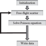
FIGURE 2.1 Typical flowchart of a particle-based device simulator.
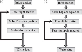
FIGURE 2.2 Philosophy behind the (a) corrected Coulomb approach, where correction force is used in the molecular dynamics routine, and (b) the fast multipole method, where the full Coulomb interaction is being considered to get the force on the electrons in the free-flight portion of the Monte Carlo transport kernel.
To avoid the problem with the k-space treatment of the Coulomb interaction, a real-space approach has been proposed by Lugli and Ferry [11] in which the electron–electron and the electron–ion interactions are accounted for via real-space molecular dynamics routine. It is important to note that direct application of the real-space molecular dynamics can be used for bulk systems only where it is not required to solve the Poisson equation. Hence, an approach is needed that correctly accounts for the full Coulomb interaction in particle-based device simulators. The group from Arizona State University (ASU) has, in that sense, been a pioneer in this field and in our simulation modules, we have currently implemented three approaches:
1. The corrected Coulomb approach—an approach that we have introduced [12].
2. The particle–particle–particle–mesh coupling method due to Hockney and Eastwood [13].
3. Fast multipole method [14].
The corrected Coulomb approach and the particle–particle–particle–mesh coupling method are similar in philosophy. Specifically, a correction force is calculated, given the mesh, and it is that correction force that is used in the molecular dynamics routine. The fast multipole method is completely different in philosophy because the Laplace equation is solved to account for the charges at the ohmic contacts, and later, only the fast multipole method is used to account for the full Coulomb interactions between the electrons and electrons and ions. The difference between these two ideologies is graphically shown in Figure 2.2.
2.3 DESCRIPTION OF THE ANALYTICAL MODELS
2.3.1 NUMBER FLUCTUATION-BASED MODEL
To PROPERLY ACCOUNT for the random number and position of the dopant ions in the depletion region of the channel, the model presented in ref. [4] accomplishes this in the following manner. The simulation domain is divided into small boxes by discretizing the channel length and width into small square cells of dimension l with a volume assisted by the depth of X that extends from the channel to ideally the maximum depletion width (depth). The random dopant ions are positioned in each of these cell volumes in random number and assortment that is based on the uniform nominal doping density. Thus, the number of dopant ions that can reside in a volume cell is dependent on the dimensions of the cell (square dimension l and depth dimension X). If this number is too small and close to unity, the calculated VT will be too small and almost invariant from cell to cell. Therefore, the volume of the cell of dimension l and X for this research is chosen so that a dopant number variation up to a maximum of 4 can be expected to reside in the cell for different random dopant distribution configurations. The required device parameters for the 45 nm physical gate length MOSFET are L (gate length) = 45 nm, W (gate width) = 50 nm, tox (oxide thickness) = 0.9 nm, and NA (substrate doping) = 8.9 × 1024 m–3. We have shown earlier that VT variation for a typical channel random dopant configuration correlates to a few nanometers in depth from the interface [15]. With the above information, the designed cell dimensions are computed to be l = 10 nm and X = 4.5 nm retrenched from the maximum possible depletion depth of Wmax = 12.34 nm. After calculating the local cell threshold voltage from its dopant number value, all the threshold voltage values from all the cells in a 2D array have been averaged to extract the final value of the threshold voltage for a particular random dopant configuration.
Once the reference VT values for different random dopant types and distributions are extracted using the procedure described in ref. [4], we have used the results from ref. [16] to calculate the threshold voltage VT fluctuation percentage for an interface trap positioned along the channel from source to drain of an effective 32 nm channel length nMOSFET. Since a single interface trap is taken to be at locations that are 2 nm apart, the length l of the cell is now reduced to 2 nm, whereas the width l is kept at 10 nm. This places a maximum of 2 atoms per cell for a particular trap to interact with. Since the random interface trap is located at the middle of the gate width, the cell left edge in the width direction is at 20 nm and the right edge is at 30 nm (where an interface trap can be found) to accommodate the required 25 nm gate width point with a margin of ±5 nm.
2.3.2 PERCOLATION-BASED ANALYTICAL MODEL
Percolation theory-based conduction through the channel of a MOSFET, as proposed by Keyes [5], takes into account the random position and distribution of channel dopants along with the interface trap underneath the active gate region, as well as the rapid surface potential fluctuations out of their local inversion conditions. In a cellular arrangement along the width, length, and depth distribution of the active channel volume, this leads to certain cells being nonconducting and certain cells being conducting. Percolation paths through conducting cells that are adjacent to one another determine the current conduction probability from source to drain along the length direction at threshold condition. The relevant set of equations as detailed in Ref. [5] is used to determine the conduction probability Q for a set of 20 random dopant-type configurations. The key term (dQ/dV) is evaluated for a particular random dopant configuration for each trap position along the source and drain (length direction) and at the middle of the gate width (width direction) of the MOSFET and at each trap position. An average is made over all 20 random dopants to arrive at the threshold voltage value for the percolation model. For the reference threshold voltage needed in the evaluation of the dV term, analytical number-based threshold voltage expressions are utilized. The percolation model threshold voltage values in the presence of random dopants and random interface traps do not deviate more than 3% from number fluctuation-based threshold voltage values. This is due to the fact that there are long arrays of cells from source to drain of a MOSFET. Thus, Q is very small (~10–4 – 10–5 range) and does not deviate appreciably as a result of the trap’s introduction and interaction with spatially inhomogeneous channel dopants and inversion carriers.
2.3.3 NEWLY PROPOSED MOBILITY FLUCTUATION-BASED ANALYTICAL MODEL WITH INHERENT NUMBER FLUCTUATION FROM DOPANTS
The models discussed in Sections 2.3.1 and 2.3.2 are inadequate in a proper replication of barrier-limited short-range interactions between a source-side trap and neighboring channel dopants and inversion carrier electrons that have been simulated by the ensemble Monte Carlo (EMC) device simulation method. From a knowledge of carrier mobility fluctuations resulting from surface potential barrier spikes at source-side trap interactions with carriers and depletion ions, the authors propose a new analytical model that incorporates low-field (threshold condition) channel mobility fluctuations in the presence of random dopants and random interface traps. In the new model, the governing equations are taken from ref. [17] with the key equation that extracts the mobility values being referenced below:
(2.1) |
From Equation 2.1, the threshold voltage VT can be determined from the known values of gds and μeff. For the calculation of gds, drain voltage bias is swept in 0.02 V increments from 0.25 to 0.45 V at a high enough gate bias of 0.8 V to cause sufficient inversion and maintain a linear region low-field approximation. The gds data are extracted from the EMC simulation for the above bias condition and the measurement of drain current. Also extracted from the EMC simulation is the surface-inverted charge Qn for the above gate voltage. The channel mobility is then calculated using ref. [18]:
(2.2) |
The value of μeff as calculated from Equation 2.2 is fed back into Equation 2.1 to calculate VT. The Vds term in Equation 2.1 is fixed at 0.4 V to reduce the DIBL (drain-induced barrier lowering) effect and excessive drain-induced charge sharing to roll off VT further.
In this section, we first present the extraction of VT for different random dopant configurations and its fluctuations induced by a single interface trap. Figure 2.3 depicts the extracted threshold voltage distribution for different random dopant configurations taking account of the two existing analytical model-based computations and EMC device simulation. Figure 2.4 shows the fluctuations in threshold voltage for different interface trap positions from source to drain of an effective 32 nm gate length MOSFET. The fluctuation trend of threshold voltage shown in this figure, for analytical model-based derivations, is compared with 3-D EMC device simulation. The results are presented in Figure 2.3. For the case of the EMC simulation method, a constant drain bias of 0.5 V is used for all threshold voltage extractions in the presence of random interface trap. Figure 2.4 illustrates the threshold voltage fluctuation extracted from an analytical model [4,6], adjusted for the trap’s interactions with channel electrons inverted at threshold conditions, and also for EMC device simulation where usual short-range interactions between the trap to an electron–electron and a trap–electron–ion are accounted for. Deviations in VT fluctuation values are noticed for the EMC simulation model in comparison with the analytical model due to the requirements of proper treatment of surface potential, mobility and inversion electron, and dopant number fluctuations through 3D short-range Coulomb force corrections. The analytical models thus exhibit inconsistencies in accurately replicating transport mechanisms existing in the vicinity of a nearby trap in the presence of random dopant ions and inversion electrons. Traps near the source end of the channel have the largest influence since they are major obstacles to the electrons because of the large input barrier experienced there. As the traps are positioned near the drain, due to the larger drift velocity and carrier excitation energy, the trap’s interaction with channel carriers is minimal and the fluctuation deviation trend is more or less within the tolerance limit.
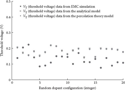
FIGURE 2.3 Threshold voltage as a function of different discrete random dopant configuration in the channel region when no interface random trap is present.
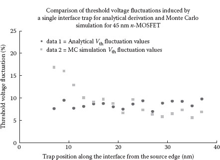
FIGURE 2.4 Threshold voltage fluctuations computed by the additional analytical model adjusted for the random interface trap’s interactions with channel electrons and the EMC simulation method.
Figure 2.5 shows the expected deviations from mean values (error-bar) for threshold voltage fluctuation percentage observed in the presence of a single interface trap positioned from source to drain for the cases of (i) an EMC-based device simulation model, (ii) an analytical number fluctuation-based model, and (iii) an EMC-based simulation method with no short-range electron–electron and an electron–ion–trap interaction force. The results presented in Figure 2.5 show the importance of consideration of a short-range electron–electron and an electron–ion–trap interaction force for a proper estimation of large fluctuation values of threshold voltage in the presence of source-side trap positions. These results highlight the importance of a short-range electron–electron and an electron–ion–trap Coulomb interaction correction to the conventional particle–mesh coupling (PM) long-range Coulomb interactions. In addition, it is evident that the traps near the source end of the channel can cause significant mobility fluctuations apart from surface potential fluctuations impeding the electron flow and enhancing the local threshold voltage variations. So, a significant mobility fluctuation needs to be added to the carrier number fluctuation for carrier electrons trapped near the source side by a random interface trap. The figure also demonstrates that as the traps are moved away from the source toward the drain end of the channel, the fluctuation pattern is within a few percentage tolerances between the analytical model and the EMC device simulation model.
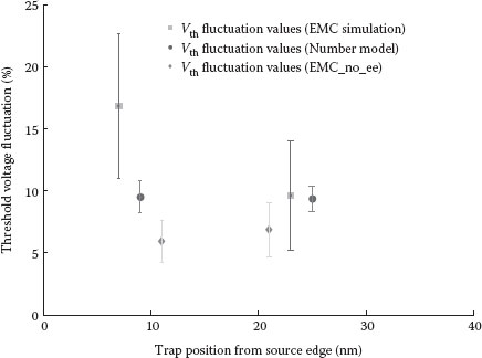
FIGURE 2.5 The error bar plot of threshold voltage fluctuation percentage for interface trap positions near the source and away from the source along the channel for the cases of (i) EMC simulation method, (ii) analytical model 1, and (iii) EMC simulation method with no short-range electron–electron and electron–ion–trap force consideration.
The newly proposed mobility fluctuation-based analytical model with its inherent incorporation of dopant number fluctuation in the channel underneath the depletion region addresses the deficiency of the number and percolation theory models, as shown in Figure 2.6. Figure 2.7 shows the statistical set of reference effective channel mobility values for the different designated types and distributions of random dopants in the channel and bulk region. Figure 2.8 shows the percentage average mobility fluctuations over a set of 20 random dopant types for the case of a single interface trap when the trap is moved from the source junction edge to the drain junction edge of the MOSFET. The variation and scatter in mobility values are due to spatially inhomogeneous channel thickness, dopant number variations (position and number in close proximity to a carrier electron), and short-range spatial electron–electron and electron–trap–ion interactions. Figure 2.9 shows the threshold voltage values for the random dopant types considered for all three analytical models and the EMC device simulation environment. Figure 2.10 shows the percentage threshold voltage fluctuations for analytical model 1 based on dopant number fluctuations in the channel [4,16], EMC device simulation method [6], and new analytical model 3 (newly proposed), respectively. The new analytical model [17,18] correctly computes channel mobility fluctuations added to dopant number fluctuations. The figure clearly reveals that model 3 (newly proposed) is more compliant to the EMC device simulation results of threshold voltage fluctuations in the vicinity of the source of an effective 32 nm channel length MOSFET. The figure also demonstrates one important observation that the dopant number fluctuations and mobility fluctuation effects cannot be considered as an additive to give rise to the actual VT fluctuation values predicted by a new analytical model. Figure 2.11 shows the error bar plot of extracted threshold voltage values for different random dopant configuration types for the cases of (i) an EMC simulation method, (ii) an analytical model 1, and (iii) a new mobility fluctuation-based model 3. Figure 2.12 further depicts the error bar plot for threshold voltage fluctuation percentage values in the presence of interface traps (source side, middle, and near drain) for all the above cases.
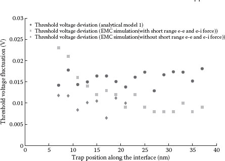
FIGURE 2.6 Threshold voltage fluctuation as a function of trap position at the interface in the channel region of the MOSFET for the first of the two analytical models and EMC simulation models with and without short-range Coulomb force corrections.
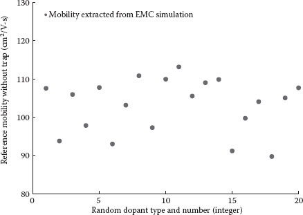
FIGURE 2.7 Effective channel mobility values for a different statistical set of random dopants. (N. Ashraf et al., Comparative analysis of mobility and dopant number fluctuations based models for the threshold voltage fluctuations estimation in 45 nm channel length MOSFET devices in the presence of random traps and random dopants, IEEE International Conference on Nanotechnology, Portland, OR, pp. 492–495, August 15–18, © (2011) IEEE. With permission.)
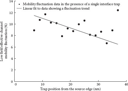
FIGURE 2.8 Effective channel mobility fluctuation as a function of trap position at the interface between source and drain junctions in the channel of the MOSFET. (N. Ashraf et al., Comparative analysis of mobility and dopant number fluctuations based models for the threshold voltage fluctuations estimation in 45 nm channel length MOSFET devices in the presence of random traps and random dopants, IEEE International Conference on Nanotechnology, Portland, OR, pp. 492–495, August 15–18, © (2011) IEEE. With permission.)
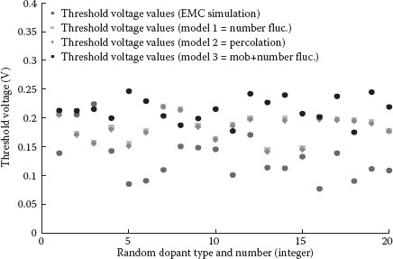
FIGURE 2.9 Threshold voltage values extracted for the two existing models in the literature along with the new analytical model and EMC device simulation for a statistical set of random dopant types designated as integer numbers. (N. Ashraf et al., Comparative analysis of mobility and dopant number fluctuations based models for the threshold voltage fluctuations estimation in 45 nm channel length MOSFET devices in the presence of random traps and random dopants, IEEE International Conference on Nanotechnology, Portland, OR, pp. 492–495, August 15–18, © (2011) IEEE. With permission.)
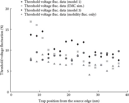
FIGURE 2.10 Percentage of averaged threshold voltage fluctuation values extracted for the two existing models in the literature along with the new analytical model and the EMC device simulation method for a single random interface trap positioned in the channel from source to drain of the MOSFET. (N. Ashraf et al., Comparative analysis of mobility and dopant number fluctuations based models for the threshold voltage fluctuations estimation in 45 nm channel length MOSFET devices in the presence of random traps and random dopants, IEEE International Conference on Nanotechnology, Portland, OR, pp. 492–495, August 15–18, © (2011) IEEE. With permission.)
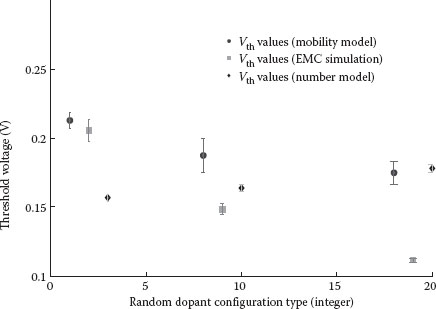
FIGURE 2.11 Threshold voltage distribution with expected deviations for different random dopant configuration types when the trap’s effect is considered.
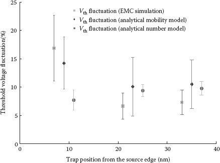
FIGURE 2.12 Threshold voltage fluctuation error bar plot considering different trap positions for the (i) EMC simulation method, (ii) analytical mobility fluctuation-based model, and (iii) analytical number fluctuation-based model.
1. K. A. Ralls, W. J. Skocpol, L. D. Jackel, R. E. Howard, L. A. Fetter, R. W. Epworth, and D. M. Tennant, Discrete resistance switching in submicron silicon inversion layers: Individual interface traps and low frequency (1/f) noise, Physical Review Letters, 52, 228–231, 1984.
2. L. Brusamarello, G. I. Wirth, and R. da Silva, Statistical RTS model for digital circuits, Microelectronics Reliability, 49(9–11), 1064–1069, 2009.
3. D. Vasileska, H. R. Khan, S. S. Ahmed, C. Ringhoffer, and C. Heitzinger, Quantum and Coulomb effects in nanodevices, International Journal of Nanoscience, 4(3), 305–361, 2005.
4. X. Tang, V. K. De, and J. D. Meindl, Intrinsic MOSFET parameter fluctuations due to random dopant placement, IEEE Transactions on Very Large Scale Integration (VLSI) Systems, 5(4), 369–376, 1997.
5. R. W. Keyes, The effect of randomness in the distribution of impurity atoms on FET thresholds, Appl. Phys. 8, 251–259, 1975.
6. W. J. Gross, D. Vasileska, and D. K. Ferry, A novel approach for introducing the electron–electron and electron–impurity interactions in particle-based simulations, IEEE Electron Device Letters 20(9), 463–465, 1999.
7. W. J. Gross, D. Vasileska, and D. K. Ferry, 3D simulations of ultra-small MOSFETs with real-space treatment of the electron–electron and electron–ion interactions, VLSI Design, 10, 437–452, 2000.
8. D. Vasileska, S. M. Goodnick, and G. Klimeck, Computational Electronics: Semiclassical and Quantum Transport Modeling, Boca Raton, FL: Taylor & Francis, June 2010.
9. M. V. Fischetti and S. E. Laux, Long-range Coulomb interactions in small Si devices, Part I: Performance and reliability, Journal of Applied Physics, 89, 1205–1231, 2001.
10. D. K. Ferry, Semiconductors, Macmillan, USA September 1, 1991.
11. P. Lugli and D. K. Ferry, Degeneracy in the ensemble Monte Carlo method for high-field transport in semiconductors, IEEE Transactions on Electron Devices, 32(11), 2431–2437, 1985.
12. W. J. Gross, D. Vasileska, and D. K. Ferry, Ultrasmall MOSFETs: The importance of the full Coulomb interaction on device characteristics, IEEE Transactions on Electron Devices, 47(10), 1831–1837, 2000.
13. R. W. Hockney and J. W. Eastwood, Computer Simulation Using Particles, New York, NY: McGraw-Hill, 1981.
14. L. Greengard and V. Rokhlin, A fast algorithm for particle simulations, Journal of Computational Physics, 135(2), 280–292, 1997.
15. W. J. Gross, D. Vasileska, and D. K. Ferry, Ultra-small MOSFETs: The importance of the full Coulomb interaction on device characteristics, 7th International Workshop IWCE, Glasgow, pp. 32–33, 2000.
16. K. Sonoda, K. Ishikawa, T. Eimori, and O. Tsuchiya, Discrete dopant effects on statistical variation of random telegraph signal magnitude, IEEE Trans. Electron Dev., 54(8), 1918–1925, 2007.
17. X. Zhou and K. Y. Lim, Unified MOSFET compact I–V model formulation through physics-based effective transformation, IEEE Trans. Electron Dev., 48(5), 887–896, 2001.
18. J. He, X. Zhang, Y. Wang, and R. Huang, New method for extraction of MOSFET parameters, IEEE Electron Dev. Lett., 22(12), 597–59 2001
19. N. Ashraf, D. Vasileska, G. Wirth, and S. Purushothaman, Comparative analysis of mobility and dopant number fluctuations based models for the threshold voltage fluctuations estimation in 45 nm channel length MOSFET devices in the presence of random traps and random dopants, IEEE International Conference on Nanotechnology, Portland, OR, pp. 492–495, August 15–18, 2011.