
Spike Timing-Dependent Plasticity Using Memristors and Nano-Crystalline Silicon TFT Memories |
CONTENTS
25.3 Synaptic Learning Mechanism
25.5.1 Spatio-Temporal Pattern Recognition
Interest in the possibility of using memristive devices as synapses in artificial neural circuits was sparked by the demonstration of TiO2 resistive switches by HP Labs in 2008 [1]. A great deal of the resulting research has been centered on implementing spike timing-dependent plasticity (STDP), which is a synaptic learning mechanism based on timing differences between action potentials [2,3]. However, time scales of biological inter-spike intervals (ISIs) are on the order of tens of milliseconds, much longer than the typical electronic phenomena. This makes STDP a difficult scheme to implement efficiently using electronics. Proposed solutions have involved pulse width or height modulation [4, 5 and 6] or pulse shaping [7] and would require somewhat extensive circuitry for each neuron. Additionally, the reports do not explain the learning characteristics beyond pair-based trials. Experiments on biological synapses indicate a much more complex reality, in that the exact mechanisms of synaptic learning cannot be explained by pair-based STDP alone [8,9]. Specifically, asymmetric temporal integration of the synaptic weight changes has been demonstrated in spike triplet and quadruplet, as well as frequency-dependent experiments [10, 11 and 12]. Progress continues on developing models that explain the observed effects more thoroughly [13,14].
Although the exact mechanisms of biological synaptic modification are not known, the consequences of STDP in large networks lead to many potential applications. For example, it is well known that STDP learning rules assist in the recognition of spatio-temporal spike patterns within a large population [15, 16 and 17]. Such behavior could be useful for recognizing recurring patterns in real-time data from large sensor streams. In addition, STDP has the ability to detect phase differences in spike patterns, which is useful for sound source localization. Finally, STDP can be used for complex visual pattern extraction. Section 25.5 discusses these examples in detail.
Other sections of this chapter describe circuits which realize a compact physical implementation of the STDP learning mechanism with biologically realistic action potentials. Simulation results of spike triplet and frequency dependence are also shown and compared to measured biological data. Complex synaptic behavior is a natural outcome of using ambipolar nano-crystalline silicon (nc-Si) thin-film transistor (TFT) memory devices in conjunction with memristive devices. As described in Section 25.2, the former can be fabricated using gold nanoparticles embedded in the gate dielectric, and the latter could be based on any number of material systems. Metal oxides such as TiO2 or HfO2 that can be deposited by atomic layer deposition (ALD) or sputtering would be preferable, however. The reason is that together with the low-temperature, large-area nc-Si deposition, these processes could enable the fabrication of a three-dimensional system with physical structure similar to the human neocortex, as illustrated in Figure 25.1. Distribution directly on top of a silicon CMOS core could be one possibility, or the rigid crystalline silicon could be completely eliminated in favor of flexible substrates.
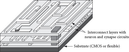
FIGURE 25.1 An illustration of arbitrarily connected neural circuits. The low-temperature processing would enable three-dimensional fabrication on top of a CMOS core, or over a large area on a flexible substrate.
Several reports of micron-scale ambipolar nc-Si TFTs exist [18,19], but the simulations in this chapter make use of the SPICE model provided in Ref. [20]. This is different from previous works [21,22] in that the model is more thoroughly vetted for submicron channel geometries. The spiking neuron circuit schematic used for the simulations is shown in Figure 25.2a, and is a heavily modified version of that originally proposed by Mead [23]. Additions of a transistor at the input and different charge leakage paths during resting or spiking (controlled by Vleak and Vreset, respectively) help to stabilize the action potential width. A more detailed description of neuron circuit operation is contained in Ref. [24]. In that work, each synapse consisted of one TFT and one memristive device, whereas here the synapses are comprised of only a single ideal memristor. The state variable w/D of the memristive device (definition provided in Ref. [1]) represents the synaptic weight. A path for potentiation current through the memristor is provided by a nanoparticle memory TFT (NP-TFT). One of these devices is placed at the output of each neuron circuit such that it would drive a large number of synapses.
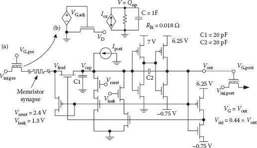
FIGURE 25.2 (a) Schematic diagram of the circuit used to investigate STDP learning. The NP-TFT for the postsynaptic neuron is actually left unconnected for these simulations. (b) The SPICE model subcircuit for the NP-TFT consists of two parts: the intrinsic transistor with adjusted gate voltage VG,adj to account for the nanoparticle charge Qnp, and an auxiliary circuit used for the trapped charge calculation.
Memory characteristics of the NP-TFT are modeled by adjusting the actual gate voltage of the intrinsic ambipolar nc-Si TFT using a dependent voltage source (VG,adj) to account for charge trapped in the nanoparticles. The total amount of trapped charge Qnp is calculated by integrating the oxide current Iox across a large capacitor. The magnitude of the oxide current is calculated based on the Poole–Frenkel equation [25] and has been closely matched to experimental data. Charge leaks off the capacitor through a small resistor, the value of which determines the time constant of retention. A schematic of the subcircuit is shown in Figure 25.2b. Testing the NP-TFT is performed via simulation as follows. The gate voltage is first quickly ramped up to the programming voltage of 4.5 V and back down, and the drain current is measured during this sweep (square symbol in Figure 25.3). Five milliseconds later, a 1 ms programming pulse (4.5 V) is applied (see Figure 25.3c), causing electrons to flow through the oxide and be trapped in the nanoparticles near the semiconductor surface. Another probing ramp 5 ms after that measures the total threshold voltage shift (circle in Figure 25.3), followed by a final probing ramp 40 ms after the programming pulse. Most of the charge has leaked off the nanoparticles by this time (triangle in Figure 25.3).
Transfer characteristics of the TFT device during each of the three ramps are shown in Figure 25.4, with symbols that correspond to those in Figure 25.3. The maximum threshold voltage shift for this device is slightly above 1 V, and charge constantly leaks off (via Rlk in Figure 25.2b) such that the retention time is in the 50–100 ms range (time constant is approximately 10 ms). The programming pulse used is similar in height and duration to the action potential output of the neuron circuit in Figure 25.2a. The SPICE model used here is based on the characteristics of recently fabricated NP-TFT devices. Depending on the gate dielectric thickness, the chosen material (SiO2 or HfO2), and the location of the nanoparticles within the dielectric, as well as the programming voltage and retention time, can be finely tuned. The intrinsic TFT used for the fabrication is the same as those of Ref. [20], though the model has a slight threshold voltage shift to generate more symmetric learning as described in the following sections. Other similar devices have also been demonstrated using organic materials [26] and amorphous silicon [27].
25.3 SYNAPTIC LEARNING MECHANISM
Changes in synaptic weight as a function of spike timing differences were measured using 100 ms transient simulations of the circuit shown in Figure 25.2a. The results of two individual simulations for pre–post and post–pre pairs are shown in Figure 25.5. The presynaptic action potential (Vgate,pre) was always applied at t = 50 ms, while the timing of the postsynaptic action potential was varied to obtain different Δt = tpost − tpre. A dependent voltage source provides the injection voltage Vinj, which is defined to be the output voltage times a multiplication factor of 0.44. Thus, Vinj will normally be near ground, but spike to ~2 V during an action potential. Timing of the postsynaptic action potential at Vout was varied using a very short 100 nA current pulse (Ipost) that was injected directly onto the node Vcap (see Figure 25.5a). Owing to the large magnitude of the current, the neuron reaches the threshold of 1.9 V almost immediately. However, it must be turned off at the instant Vfeed reaches 1.9 V to avoid inducing errors in the synaptic weight measurement, and the time at which it turns off is recorded as tpost. Also, the current source must be placed at Vcap and injected directly onto the “membrane” capacitor C1. If it is placed at the Vfeed node, too much reverse current will flow when the feed transistor starts to turn off, which will artificially increase potentiation, resulting in an erroneous STDP curve. Careful observation of the circuit operation is therefore necessary when evaluating the performance of the system and subsequent synaptic weight changes.
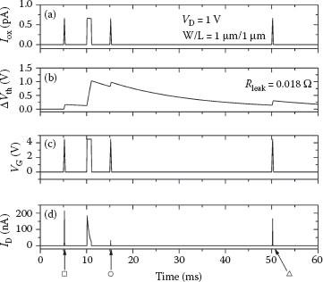
FIGURE 25.3 Traces of (a) current through the gate dielectric Iox, (b) the threshold voltage shift as a function of time, (c) applied gate voltage VG, and (d) drain current ID through the NP-TFT. A fast gate voltage sweep is used to probe ID–VG immediately before and after the programming pulse (which occurs at t = 10 ms) then again at 40 ms later after the charge has leaked from the nanoparticles. The three labeled probing regions correspond to the symbols in Figure 25.4.
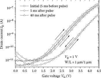
FIGURE 25.4 Transfer characteristics of the NP-TFT immediately prior to, 5 ms after, and 40 ms after the programming pulse (presynaptic action potential VG). These curves correspond to the drain current measured during the three gate voltage probing sweeps shown in Figure 25.3.
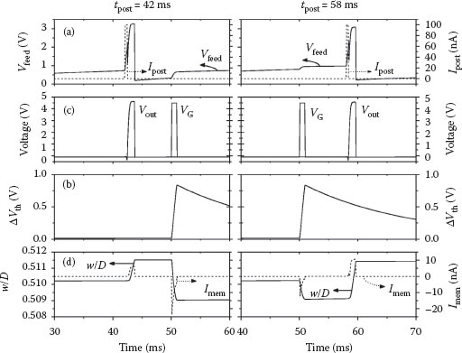
FIGURE 25.5 Pair-based STDP testing procedure. The left column is a post–pre pair resulting in overall synaptic depression, whereas the right-hand column is a potentiating pre–post pair. (a) The voltage at the input node of the postsynaptic neuron Vfeed, along with the injection current Ipost required to generate an action potential. (b) The output voltage Vout of the postsynaptic neuron (see Figure 25.2a along with the gate voltage applied to the NP-TFT. This voltage VG induces trapped charge in the nanoparticles, resulting in the threshold voltage shifts shown in (c). (d) The current through the memristive device Imem, the magnitude of which relates to the change in the state variable w/D, and thus the synaptic weight.
In addition to the current pulse injected into the postsynaptic neuron to initiate spikes at precise times, a constant DC current Ipost,DC was added to imitate the excitation of the neuron by many other afferents. This current causes the voltage Vfeed to build up and be greater than zero, but is set less than the leakage current so it does not cause the neuron to fire. Under realistic operating conditions, the summation of many different excitatory postsynaptic potentials (EPSPs) will generate approximately the same effect [24]. During a presynaptic action potential, the memory TFT is on and forward current flows through the memristor to the postsynaptic neuron, decreasing the synaptic weight. The magnitude of the decrease depends not only on the magnitude of the injection voltage (Vinj ≈ 2 V) but also on the instantaneous value of Vfeed. If the postsynaptic neuron is nearly at threshold (~1.9 V), there is almost no voltage drop across the memristor and thus very little depression. Dependence of the weight change on the postsynaptic voltage is also a characteristic of biological synapses [13,28].
Upon termination of the presynaptic action potential, the memory transistor channel remains on for an extended period while the trapped charge leaks away. The length of time between the initial presynaptic pulse and the postsynaptic neuron action potential controls the reverse current through the memristor, and thus the potentiation (Figure 25.5d). In other words, the magnitude of the weight increase varies with the instantaneous conductance of the TFT channel at the time of the postsynaptic spike. Although somewhat difficult to see in Figure 25.3b, a continuous application of presynaptic pulses will shift the threshold voltage beyond 1 V. Therefore, the potentiation is not necessarily dependent only on the nearest-neighbor spike interaction, but will in fact be stronger if several presynaptic action potentials occur immediately prior to a post spike [29].
The results of performing many trials of post–pre (left column of Figure 25.5) and pre–post (right column of Figure 25.5) are shown in Figure 25.6. Different DC injection currents of 0.5, 1, and 1.5 nA are shown in Figure 25.6a, b, and c, respectively, each with different values of the initial synaptic weight (w/D = 0.2, 0.5, and 0.8). The similarity to biological measurements such as those reported in Ref. [2] is striking, especially for the case that Ipost,DC = 1 nA. Dependence of the weight change on the initial weight is also observed in biology, but a more detailed analysis is required to determine if the trends are the same in these circuits [30]. The value of Vfeed in these simulations varies depending on how long the postsynaptic action potential occurred before that of the presynaptic neuron because Vfeed is reset after the spike. It then slowly builds up to different levels at tpre = 50 ms. In simulations of the pre–post pair, Vfeed is always the same value at the tpost because it is not reset until that point (see the right-hand column of Figure 25.5a).
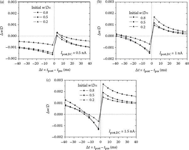
FIGURE 25.6 Pair-based STDP curves for various initial synaptic weight values (w/D) and DC postsynaptic injection currents Ipost,DC. The different values of (a) 0.5 nA, (b) 1 nA, and (c) 1.5 nA vary the voltage Vfeed at the time of the first spike. Each data point is obtained from individual simulations like those shown in Figure 25.5.
In a manner similar to the previous section with action potential pairs, the synaptic weight changes resulting from spike triplets were obtained. Temporal plots of the main circuit variables analogous to Figure 25.5 are shown in Figure 25.7. In all of the cases, a 1 nA DC injection current was used. Data for a full set of triplets are shown in Figure 25.8, with a direct comparison to biological measurements [11] and the model of Clopath and Gerstner [13]. Although there is some difference in the actual levels of potentiation, the overall trend for potentiation and depression is very well-matched.
A final experiment involves testing the changes in synaptic weight as a function of the frequency of applied action potentials. With Δt set to specific positive values, the pairs are repeated 10 times at different frequencies. The periods are kept larger than Δt so that the spike train is always pre–post alternating. Depending on the frequency, the postsynaptic spike may occur at varying times during the duty cycle of tpre, as shown in the insets of Figure 25.9. Specifically, in the upper inset, the majority of the pairs look like post–pre sequences, whereas at a lower frequency for the same Δt, they are clearly pre–post (lower inset). The weight change is positive in the former case because the NP-TFT channel essentially stays on for the duration of the stimulus, resulting in synaptic potentiation. In the latter case, depression dominates because the DC injection current is set to 0 nA in this simulation. If it is larger, potentiation occurs for all frequencies when the pairs are pre–post alternating.
Simulations using trains of post–pre pairs were also performed (not shown). The curves generated were similar in shape to those of Figure 25.9, but with more dominant depression at low frequencies. At high frequencies, however, there is still strong potentiation. From a Hebbian perspective, the relationship makes sense because concurrent high-frequency activity should strengthen the neuronal connection regardless of the exact timing. Very similar behavior and curve shapes have been widely reported in biological measurements [10,31,32].
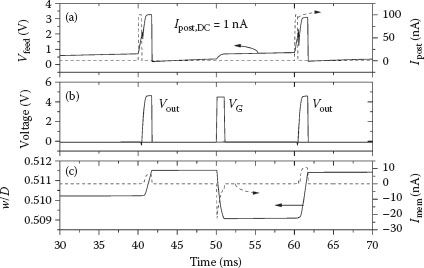
FIGURE 25.7 Plots of different circuit variables as a function of time during a (10,−10) post–pre–post triplet test. (a) The injection current pulses Ipost quickly increase Vfeed to the threshold, causing the postsynaptic neuron to fire at t = 40 and 60 ms. These action potentials are shown together with the presynaptic spike VG in (b). (c) Current through the memristive device Imem alters the synaptic weight w/D as a function of time by an amount proportional to the polarity and the magnitude. This triplet results in overall synaptic potentiation.
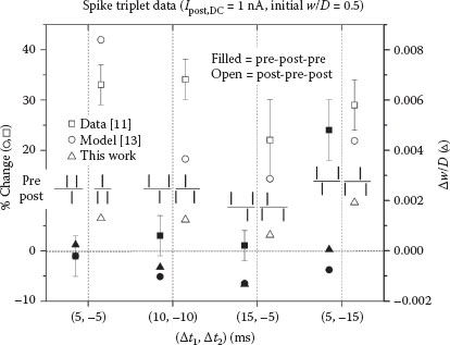
FIGURE 25.8 A direct comparison of synaptic weight changes in spike triplet experiments between Refs. [11] and [13] and this work. The biological data taken in the hippocampus cells indicate dominance of synaptic potentiation.
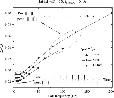
FIGURE 25.9 Frequency dependence of the synaptic weight change for different Δt values. Ten action potential pairs were applied at different frequencies with the given pre–post offset, and the total weight change was measured. The insets show approximately what the pre- and postsynaptic firing looks like for different regions of the graph.
Further analysis is warranted regarding some issues related to the devices and circuits described in this work. The first calculates the approximate power dissipation of the individual components and the system, and compares that to the human brain. It can be seen in Figure 25.7c that the current flow through the memristor during any action potential (pre- or postsynaptic) is on the order of 10 nA given the voltages used. Also, the memristor state variable in this case was w/D = 0.5, which corresponds to Rmem = 25 MΩ. At this value, the average energy per synapse per spike (with 1 ms duration) is ~2.5 pJ. There is no power dissipation of the synapse when neither the pre- nor postsynaptic neurons are in the nonfiring state. Measurements made on a fabricated neuron circuit indicate that the total power consumption, including in standby mode (nonfiring), is ~12 nW at 100 Hz. Now imagine a system with the same scale as that of the human neocortex (1010 neurons [33] and 1014 synapses [34]). Assuming that all the synapses are at the same weight of w/D = 0.5 and an overall average firing rate of 100 Hz, the total power consumption approaches 25 kW, most of which is in the synapses. This value is clearly far too large for any realistic electronic system, but could easily be reduced by a factor of 100 or more with some simple design alterations. This would put the total power requirement at approximately the same magnitude as the human brain [35].
Reduction of the injection voltage Vinj would be the main factor that significantly diminishes the amount of current flowing through the memristive devices. It is currently set to approximately 2 V (0.44 × Vout) because the value must be greater than the threshold of the input inverter (~1.9 V) in order for the postsynaptic neuron to fire. In other words, the maximum value that Vcap could ever obtain is the same as Vinj (see Figure 25.2a). Reducing the value of Vinj to 0.2 V or less would be ideal from the power reduction perspective as well as a fan-in and density viewpoint. With reduced Vinj, a much smaller input capacitor C1 could be used to obtain the same voltage at Vcap. One possible method to obtain such low-voltage operation could be the addition of a front-end amplifier to translate ~100 mV at Vcap into the ~1.9 V necessary to trip the inverter. Along the same lines, reducing the device threshold voltage [36] and optimizing the inverter transfer curve would allow much lower power supply voltages and switching currents. Another point to be made is that even after significant improvements, the required power may still be too much for a small chip, but could easily be dissipated over larger areas.
Bias degradation of the nc-Si silicon TFT devices is an additional matter of concern [37]. There is some research that addresses the circuit-level impact of TFT degradation [38], but none specifically targeting neuromorphic circuits and systems. However, increased deposition temperatures will produce more stable nc-Si films, leading to reduced threshold voltage shift over time [39]. In turn, the neuron circuit operation should remain relatively stable, and an advantage of this architecture would be the ability to adapt to changes in the firing rate, pulse width, and so on. Future measurements should confirm the expectation that device degradation will not significantly impact on the overall operation of these systems.
Although pair-based STDP fails to explain all the effects observed in biology, it remains a fundamental first-order approximation of true learning rules. Potential applications for a hardware implementation of the STDP learning rule are outlined in this section. Fundamental system-level consequences of STDP are explained first, followed by the applications. In the first case, a methodology for performing spatio-temporal pattern recognition is shown, having potential use for real-time processing of large amounts of input data. Described next is sound source localization via detection of interaural time differences, which is a capability of animals that can be attributed to STDP learning rules. Finally, the extraction of features such as edges from visual scenes is discussed. Other applications that have been investigated previously but are not explicitly included here are pattern recall [40] and dataset classification [41].
25.5.1 SPATIO-TEMPORAL PATTERN RECOGNITION
It has been recognized for some time that when implemented as single layer perceptron networks, STDP learning rules enable the identification of recurring spike patterns [15, 16 and 17]. Because the patterns are time-resolved and distributed within a subset of the afferent neurons located in space, this is generally referred to as spatio-temporal pattern recognition. Theoretical studies consist of randomly generated afferent spike trains with Poisson-distributed ISI. At specific times, a fraction of the population of input neurons simultaneously produces unique patterns, and the output neuron learns over time to respond only to these presentations. The recurring patterns are the same each time they occur for a particular neuron, but different between neurons. They are also generated such that the firing rate remains approximately constant so as not to be distinguished in this way. At first, the output neuron responds randomly to the input spike trains and is not selective to the recurring patterns. After some time (or a certain number of pattern presentations), the synaptic weights are altered such that the output responds quickly to the start of the pattern. The STDP learning rule controls the weight change and there is no supervision or training of the network. Successful identification of the simultaneous patterns increases with the frequency of their presentation, the proportion of afferents involved, and the high precision firing times within the pattern (low jitter) [17].
In a single layer, the spatio-temporal pattern recognition is interesting but not particularly useful. Connected with multiple layers in a hierarchical structure, far more complex patterns, or even the absence of patterns, could be detected. These systems would be useful for any application involving the real-time processing of large amounts of data that contain recurring temporal patterns. Examples might include large sensor networks connected to electronic systems or networks to detect errors or intrusions, power grids to proactively prevent faults, or to traffic monitoring systems to efficiently route cars or emergency vehicles.
The ability to identify the spatial position of a sound source is an important aspect of animal perception. At frequencies in which the wavelength is shorter than the spacing of the ears, interaural intensity difference is typically used to locate sounds. When the wavelength is longer, the interaural time difference (ITD) is detected to precisely locate the source on the azimuthal plane. Coincidence detection properties of neurons and the STDP learning rule are both utilized in the auditory system to perform sound localization [42, 43 and 44]. The neuron circuits in this work function as integrators or coincidence detectors depending on the action potential frequency [24,45].
In owls, the ability to detect ITDs of down to a few microseconds corresponds to angular precision of a few degrees, helping these nocturnal birds locate prey by sound alone. Other animals such as bats and dolphins use echolocation for navigation and to detect and avoid nearby objects. Essentially the same mechanisms can be used in engineered systems such as robots and autonomous vehicles to assist in navigation. A distinct advantage to using neural networks to perform this task is not only the efficiency, but also the possibility of integrating these data with that from other sensor systems (for instance, an artificial visual cortex as described in Section 25.5.3) to more fully comprehend the contents of the surrounding environment. In addition, one could imagine modules for various electronic systems that incorporate this localization technology, helping microphones to pick out the location of a voice when there is a noisy background. Again, the potential to efficiently integrate this system directly with another capability such as speech recognition is a distinct advantage of these networks.
The visual cortex is the most densely connected area of the human cortex [46]. It performs many complex processing operations. One known function is orientation sensitivity, and the ability to detect edges of objects within the visual field. The emergence of this capability is a consequence of STDP [47, 48 and 49], and several studies have been devoted to emulating it using electronic devices [50, 51 and 52]. Toward the overall goal of building an artificial visual cortex that can process complete visual scenes and return information in real time, interim applications could include the recognition and classification of specific images. Recognizing handwriting [52], faces [51], and the locations of nearby cars traveling down a highway [50] are examples of tasks that digital systems have difficulty in performing successfully. Artificial neural networks promise to provide the ability to efficiently differentiate between similar letters or distinguish faces with subtle variations in the shapes of noses or eyes. They will also be able to classify cars, trucks, and motorcycles into distinct categories. And perhaps the most important feature inherent in these systems will be no requirement for programming or explicitly training the network to perform such a wide variety of functions.
Neuron circuits comprising of ambipolar nc-TFTs and NP-TFTs are simulated using SPICE. Single memristive devices are used for the synapses, and are driven by the NP-TFTs connected to the presynaptic neuron outputs. Using this compact configuration, the circuits exhibit timing-dependent synaptic learning with biologically realistic action potentials (no changes in the height or width, and no pulse shaping is required). The striking similarity to biological synapses is demonstrated through pair- and triplet-based experiments, as well as in the frequency dependence of the weight changes. The significance of these results is highlighted by the use of materials and devices which could conceivably be used to build dense, large-scale systems with 3-D physical structure similar to the neocortex.
Beyond the investigation of the learning mechanisms, considerable discussion was devoted to other important issues. These include improving the circuit performance for use in large networks, reducing power consumption, and mitigating concerns about device and circuit reliability. Three potential applications of these circuits were also presented in detail. One consequence of STDP, the ability of the network to respond to recurring spatio-temporal patterns, may be very useful for systems that must process large amounts of input data streaming in real time. Sound localization can also be accomplished by taking advantage of the timing-dependence of the learning to detect phase differences in aural signals. An artificial visual cortex capable of extracting and processing visual information such as edges in multiple receptive fields is the last of the applications discussed. With such a rich set of capabilities and applications, it should be clear that artificial neural networks employing STDP learning have great potential for future electronic systems that could help provide humans with more detailed and useful information about the complex environment around them.
1. D. B. Strukov, G. S. Snider, D. R. Stewart, and R. S. Williams, The missing memristor found, Nature, 453(7191), 80–83, 2008.
2. G.-Q. Bi and M.-M. Poo, Synaptic modification by correlated activity: Hebb’s postulate revisited, Annual Review of Neuroscience, 24, 139–166, 2001.
3. S. Song, K. D. Miller, and L. F. Abbott, Competitive Hebbian learning through spike-timing-dependent synaptic plasticity, Nature Neuroscience, 3(9), 919–926, 2000.
4. G. S. Snider, Spike-timing-dependent learning in memristive nanodevices, in IEEE International Symposium on Nanoscale Architectures (NANOARCH) Anaheim, CA, 2008, pp. 85–92.
5. S. H. Jo, T. Chang, I. Ebong, B. B. Bhadviya, P. Mazumder, and W. Lu, Nanoscale memristor device as synapse in neuromorphic systems, Nano Letters, 10(4), 1297–1301, 2010.
6. D. Kuzum, R. G. D. Jeyasingh, B. Lee, and H. S. P. Wong, Nanoelectronic programmable synapses based on phase change materials for brain-inspired computing, Nano Letters, 12(5), 2179–2186, 2011.
7. B. Linares-Barranco and T. Serrano-Gotarredona, Exploiting memristance in adaptive asynchronous spiking neuromorphic nanotechnology systems, in 9th IEEE Conference on Nanotechnology (IEEE NANO), Genoa, Italy, 2009, pp. 601–604.
8. J. Lisman and N. Spruston, Questions about STDP as a general model of synaptic plasticity, Frontiers in Synaptic Neuroscience, 2(140), 2010. DOI: 10.3389/fnsyn.2010.00140.
9. H. Z. Shouval, S. S. H. Wang, and G. M. Wittenberg, Spike timing dependent plasticity: A consequence of more fundamental learning rules, Frontiers in Computational Neuroscience, 4(19), 2010. DOI: 10.3389/fncom.2010.00019.
10. H. Markram, J. Lubke, M. Frotscher, and B. Sakmann, Regulation of synaptic efficacy by coincidence of postsynaptic APs and EPSPs, Science, 275(5297), 213–215, 1997.
11. H.-X. Wang, R. C. Gerkin, D. W. Nauen, and G.-Q. Bi, Coactivation and timing-dependent integration of synaptic potentiation and depression, Nature Neuroscience, 8, 187–193, 2005.
12. R. C. Froemke and Y. Dan, Spike-timing-dependent synaptic modification induced by natural spike trains, Nature, 416, 433–438, 2002.
13. C. Clopath and W. Gerstner, Voltage and spike timing interact in STDP—A unified model, Frontiers in Synaptic Neuroscience, 3(25), 2010. DOI: 10.3389/fnsyn.2010.00025.
14. C. G. Mayr and J. Partzsch, Rate and pulse based plasticity governed by local synaptic state variables, Frontiers in Synaptic Neuroscience, 2(33), 2010. DOI: 10.3389/fnsyn.2010.00033.
15. W. Gerstner, R. Ritz, and J. van Hemmen, Why spikes? Hebbian learning and retrieval of time-resolved excitation patterns, Biological Cybernetics, 69(5), 503–515, 1993.
16. R. Guyonneau, R. VanRullen, and S. J. Thorpe, Neurons tune to the earliest spikes through STDP, Neural Computation, 17(4), 859–879, 2005.
17. T. Masquelier, R. Guyonneau, and S. J. Thorpe, Spike timing dependent plasticity finds the start of repeating patterns in continuous spike trains, PLoS ONE, 3(1), e1377, 2008. DOI:10.1371/journal. pone.0001377.
18. C.-H. Lee, A. Sazonov, M. R. E. Rad, G. R. Chaji, and A. Nathan, Ambiploar thin-film transistors fabricated by PECVD nanocrystalline silicon, in Materials Research Society Spring Meeting Proceedings, San Francisco, CA, 2006.
19. K.-Y. Chan, J. Kirchhoff, A. Gordijn, D. Knipp, and H. Stiebig, Ambipolar microcrystalline silicon thinfilm transistors, Thin Solid Films, 517(23), 6383–6385, 2009.
20. A. Subramaniam, K. D. Cantley, H. J. Stiegler, R. A. Chapman, and E. M. Vogel, Submicron ambipolar nanocrystalline silicon thin-film transistors and inverters, IEEE Transactions on Electron Devices, 59(2), 359–366, 2011.
21. K. D. Cantley, A. Subramaniam, H. J. Stiegler, R. A. Chapman, and E. M. Vogel, SPICE simulation of nanoscale non-crystalline silicon TFTs in spiking neuron circuits, in 53rd IEEE International Midwest Symposium on Circuits and Systems (MWSCAS), Seattle, WA, 2010, pp. 1202–1205.
22. K. D. Cantley, A. Subramaniam, H. J. Stiegler, R. A. Chapman, and E. M. Vogel, Hebbian learning in spiking neural networks with nano-crystalline silicon TFTs and memristive synapses, IEEE Transactions on Nanotechnology, 10(5), 1066–1073, 2011.
23. C. Mead, Analog VLSI and Neural Systems. New York: Addison-Wesley, 1989.
24. K. D. Cantley, A. Subramaniam, H. J. Stiegler, R. A. Chapman, and E. M. Vogel, Neural learning circuits utilizing nano-crystalline silicon transistors and memristors, IEEE Transactions on Neural Networks and Learning Systems, 23(4), 565–573, 2012.
25. S. M. Sze, Physics of Semiconductor Devices, 3rd Ed. Hoboken, NJ: John Wiley and Sons, 2007.
26. F. Alibart, S. Pleutin, D. Guérin, C. Novembre, S. Lenfant, K. Lmimouni, C. Gamrat, and D. Vuillaume, An organic nanoparticle transistor behaving as a biological spiking synapse, Advanced Functional Materials, 20(2), 330–337, 2010.
27. Y. Kuo and H. Nominanda, Nonvolatile hydrogenated-amorphous-silicon thin-film-transistor memory devices, Applied Physics Letters, 89(173503), 2006. DOI: 10.1063/1.2356313.
28. J. M. Brader, W. Senn, and S. Fusi, Learning real-world stimuli in a neural network with spike-driven synaptic dynamics, Neural Computation, 19(11), 2881–2912, 2007.
29. A. Morrison, M. Diesmann, and W. Gerstner, Phenomenological models of synaptic plasticity based on spike timing, Biological Cybernetics, 98(6), 459–478, 2008.
30. M. C. W. van Rossum, G. Q. Bi, and G. G. Turrigiano, Stable Hebbian learning from spike timing-dependent plasticity, The Journal of Neuroscience, 20(23), 8812–8821, 2000.
31. J.-P. Pfister and W. Gerstner, Triplets of spikes in a model of spike timing-dependent plasticity, The Journal of Neuroscience, 26(38), 9673–9682, 2006.
32. P. J. Sjostrom, G. G. Turrigiano, and S. B. Nelson, Rate, timing, and cooperativity jointly determine cortical synaptic plasticity, Neuron, 32(6), 1149–1164, 2001.
33. B. Pakkenberg and H. J. G. Gundersen, Neocortical neuron number in humans: Effect of sex and age, The Journal of Comparative Neurology, 384(2), 312–320, 1997.
34. Y. Tang, J. R. Nyengaard, D. M. G. DeGroot, and H. J. G. Gundersen, Total regional and global number of synapses in the human brain neocortex, Synapse, 41(3), 258–273, 2001.
35. D. Attwell and S. B. Laughlin, An energy budget for signaling in the grey matter of the brain, Journal of Cerebral Blood Flow and Metabolism, 21(10), 1133–1145, 2001.
36. A. Subramaniam, K. D. Cantley, R. A. Chapman, H. J. Stiegler, and E. M. Vogel, Submicron ambipolar nanocrystalline-silicon TFTs with high-κ gate dielectrics, in International Semiconductor Device Research Symposium (ISDRS), College Park, MD, 2011.
37. M. J. Powell, S. C. Deane, and W. I. Milne, Bias-stress-induced creation and removal of dangling-bond states in amorphous silicon thin-film transistors, Applied Physics Letters, 60(2), 207–209, 1992.
38. D. R. Allee, L. T. Clark, B. D. Vogt, R. Shringarpure, S. M. Venugopal, S. G. Uppili, K. Kaftanoglu, H. Shivalingaiah, Z. P. Li, J. J. Ravindra Fernando, E. J. Bawolek, and S. M. O’Rourke, Circuit-level impact of a-Si:H thin-film-transistor degradation effects, IEEE Transactions on Electron Devices, 56(6), 1166–1176, 2009.
39. A. Subramaniam, K. D. Cantley, R. A. Chapman, B. Chakrabarti, and E. M. Vogel, Ambipolar nanocrystalline-silicon TFTs with submicron dimensions and reduced threshold voltage shift, in 69th Annual Device Research Conference (DRC) Digest, Santa Barbara, CA, 2011.
40. J. Arthur and K. Boahen, Learning in silicon: Timing is everything, Advances in Neural Information Processing Systems, 18, 75–82, 2006.
41. L. Bako, Real-time classification of datasets with hardware embedded neuromorphic neural networks, Briefings in Bioinformatics, 11(3), 348–363, 2010.
42. C. E. Carr and M. Konishi, A circuit for detection of interaural time differences in the brain stem of the barn owl, The Journal of Neuroscience, 10(10), 3227–3246, 1990.
43. B. Glackin, J. A. Wall, T. M. McGinnity, L. P. Maguire, and L. J. McDaid, A spiking neural network model of the medial superior olive using spike timing dependent plasticity for sound localization, Frontiers in Computational Neuroscience, 4(18), 2010. DOI: 10.3389/fncom.2010.00018.
44. W. Maass and C. M. Bishop, Pulsed Neural Networks. Cambridge, MA: The MIT Press, 1999.
45. P. König, A. K. Engel, and W. Singer, Integrator or coincidence detector? The role of the cortical neuron revisited, Trends in Neurosciences, 19(4), 130–137, 1996.
46. E. R. Kandel, J. H. Schwartz, and T. M. Jessell, Principles of Neural Science, Fourth ed. New York: McGraw-Hill, 2000.
47. A. Delorme, L. Perrinet, and S. J. Thorpe, Networks of integrate-and-fire neurons using Rank Order Coding B: Spike timing dependent plasticity and emergence of orientation selectivity, Neurocomputing, 38(40), 539–545, 2001.
48. T. Masquelier and S. J. Thorpe, Unsupervised learning of visual features through spike timing dependent plasticity, PLoS Computational Biology, 3(2), e31, 2007.
49. S. Thorpe, A. Delorme, and R. Van Rullen, Spike-based strategies for rapid processing, Neural Networks, 14(6–7), 715–725, 2001.
50. M. Suri, O. Bichler, D. Querlioz, O. Cueto, L. Perniola, V. Sousa, D. Vuillaume, C. Gamrat, and B. DeSalvo, Phase change memory as synapse for ultra-dense neuromorphic systems: Application to complex visual pattern extraction, in International Electron Devices Meeting (IEDM), Washington, DC, 2011, pp. 11–79–11–82.
51. B. Linares-Barranco, T. Serrano-Gotarredona, L. A. Camuas-Mesa, J. A. Perez-Carrasco, C. Zamarreo-Ramos, and T. Masquelier, On spike-timing-dependent-plasticity, memristive devices, and building a self-learning visual cortex, Frontiers in Neuroscience, 5(26), 2011. DOI: 10.3389/fnins.2011.00026.
52. G. S. Snider, Self-organized computation with unreliable, memristive nanodevices, Nanotechnology, 18(365202), 2007.