
Analysis of Yield Improvement Techniques for CNFET-Based Logic Gates |
CONTENTS
43.3.2 Metallic CNTs Are Present
43.3.3 Metallic CNTs Are Being Removed
Carbon nanotubes are hollow cylinders in which carbon atoms are arranged in the honeycomb lattice [1]. They were first demonstrated by Bethune [2] and Iijima [3] in 1993. Carbon nanotubes have found numerous applications in nanoelectronics because of their superior electronic properties.
Single-walled carbon nanotube field-effect transistors (CNFETs) are promising candidates for future integrated circuits [1,4] because of their excellent properties, like the long scattering mean free path (MFP) >1 μm [5], resulting in near ballistic transport [6], high carrier mobilities (103 ~ 104 cm2/Vs) in semiconducting carbon nanotubes (CNTs) [7], and the easy integration of high-k dielectric material such as HfO2 [8], or ZrO2 [9], that improve gate electrostatics. Owing to the aforementioned properties, CNFETs have the potential to deliver higher performance and lower power as compared to FETs built in silicon technology [10,11].
The 1-D structure of metallic carbon nanotubes allows the electrons to travel without scattering for long distances. The mean free path of metallic CNTs is estimated to be 1000 nm [1], 25 times longer than the mean free path of copper interconnects that is equal to 40 nm at room temperature. Moreover, the current carrying capacity of metallic carbon nanotubes is almost 1010 (A/cm2) [12] and is several orders of magnitude larger than the current carrying capacity of copper interconnects. These potential advantages of metallic carbon nanotubes make them a suitable candidate for future interconnects as well as vertical vias.
On-chip capacitors are required in certain analog circuits and for decoupling purposes in digital circuits. Current integrated circuit technology uses metal–insulator–metal (MIM) and metal oxide semiconductor (MOS) capacitors as decoupling capacitors. However, the major problem with this approach is the small capacitance per unit area. Owing to of their low resistivity at nanoscale dimensions, carbon nanotubes have a great potential to be used as integrated capacitors in future integrated circuits [13]. Researchers have shown that the use of CNT-based integrated capacitors significantly increases the capacitance per unit area as well as the quality factors as compared to the capacitors fabricated with MIM and MOS technology [14,15].
Carbon nanotubes can also be used as on-chip inductors [16,17] because of their smaller footprint, higher drive current, and smaller curvatures. Recent research works have shown promising results for the use of CNTs as passive inductors in low-noise amplifiers (LNA) [18].
In addition to the excellent electronics properties, carbon nanotubes have excellent mechanical properties. Their mechanical strength makes them potential candidates for being used in flexible electronics. Various groups have reported the fabrication of individual CNFETs [19] and CNFET-based circuits [20] on flexible substrates with performance ranging from 40 MHz to 6 GHz.
The focus of this chapter is on the application of carbon nanotubes as a channel material for building CNFETs because of their potential of providing large performance advantage over Si complementary metal oxide semiconductor (CMOS) devices. Figure 43.1 shows a cross section and top view of a CNFET with an array of four single-wall (SW) CNTs used as a channel material. Carbon nanotubes are grown by chemical synthesis, and therefore it is very difficult to obtain the precise control on the exact positioning and chirality of CNTs during their growth. In this work, we have analyzed the impact of the unwanted growth of metallic tubes on the performance, power, and yield of CNFET-based circuits. Moreover, we propose solutions to build robust CNFET-based circuits with reduced variability in the performance and power in the presence of fabrication imperfections. It was reported that under ideal conditions, CNFETs are 13 times faster than a p-channel metal oxide semiconductor (PMOS) transistor and 6 times faster than an n-channel metal oxide semiconductor (NMOS) transistor [21] built in 32 nm technology node. To harness these performance advantages, the challenges listed below need to be overcome:
1. Variation in the diameter of tubes
2. Misalignment of CNTs during the fabrication of CNTs
3. The unwanted growth of metallic tubes
These carbon nanotube fabrication imperfections adversely impact the performance, power, and yield of circuits designed with carbon nanotube-based transistors. The variation in the diameter of tubes results in a variation in the drive current of CNFET, and therefore impacts the performance of CNFET-based circuits. The lack of precise control on the positioning of CNTs during the fabrication of CNFETs can result in a misalignment of the tubes [22]. Significant progress has been made in the fabrication of aligned CNTs, and less than 0.5% of CNTs fabricated on the single-crystal quartz substrate are misaligned [23]. The misaligned tubes can cause either a short between the output and the supply rail, or an incorrect logic function. Recently, efficient layout techniques have been proposed to tackle this problem [24]. The presence of metallic tubes creates an ohmic short between the source and drain of a CNFET and thus has a detrimental impact on the delay, static power, and functional yield of logic gates. Current CNT synthesis techniques produce between 4% and 40% [25,26] metallic tubes.
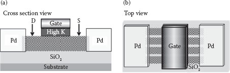
FIGURE 43.1 (a) Cross section of CNFET. (b) Top view of CNFET with an array of four CNTs. (R. Ashraf et al., Analysis of yield improvement techniques for CNFET-based logic gates, 2011 11th IEEE Conference on Nanotechnology (IEEE-NANO), August 15–18, pp. 724–729. © (2011) IEEE. With permission.)
In this chapter, our focus is on analyzing the impact of diameter variation and the presence of metallic tubes on the functional yield of CNFET-based logic gates. The percentage of metallic tubes falls roughly into two ranges: a range for which robust CNT-based circuits can be implemented with circuit-level techniques, and a range for which extra processing techniques are required to remove the metallic tubes. We will analyze and identify these ranges.
As mentioned in the previous section, the major challenges faced by the CNFET technology are variation in the diameter of tubes, misalignment of CNTs during the fabrication of CNFETs, and the unwanted growth of metallic tubes. The diameters of typically fabricated CNTs show a Gaussian distribution [27] and vary between 1 and 2 nm [28]. The diameter of the tubes impacts the bandgap of CNTs, which then impacts the drive current of CNFETs. Tubes with a smaller diameter have a large bandgap and therefore smaller ON and OFF currents, whereas tubes with a larger diameter have higher ON and OFF currents. Therefore, a variation in the diameter of tubes leads to a variation in the performance (delay) of CNFETs. To reduce this variation and increase the drive current, researchers have proposed to create multiple parallel transport paths [23] by using an array of densely packed CNTs as a channel material.
Monte Carlo simulations are performed to obtain the sigma-to-mean ION and IOFF currents as a function of the number of parallel CNTs (Ntur) in a transistor with the assumption that all the tubes are present and semiconducting. A sample size (n) of 10,000 transistors is used for Monte Carlo simulations. Simulation results showed that the σ/μ variation in the ON and OFF currents decreases by increasing the number of tubes in the transistor. The maximum variation obtained in the ON and OFF currents is almost 10%, and 3.5 times and this is obtained for Ntur = 1. Similarly, the minimum variation obtained in the ON and OFF currents is almost 2% and 0.5 times and this is obtained for Ntur = 32. This decrease in variations while increasing the number of parallel CNTs is due to the statistical averaging of currents among the multiple tubes of the transistors [29].
Although the grown CNTs are well aligned, a small percentage of CNTs can still end up being misaligned. The misalignment of tubes can cause incorrect logic functionality of gates. Recently, new layout techniques to design circuits such that misaligned tubes can be easily etched out have been proposed [24,30]. These techniques ensure the correct functionality of logic gates in the presence of misaligned tubes. The proposed layouts introduce small overheads of the area and delay. In this work, we assume that the misalignment of tubes is corrected by proper layout designs of CNFET-based gates, and therefore the tube misalignment problem is eliminated and the array of CNTs is perfectly aligned.
To use CNTs as the channel material, only semiconducting CNTs are required. However, as was mentioned earlier, depending on the chirality, an SW-CNT can be either metallic or semiconducting. At present, there is no CNT synthesis technique that can produce 100% semiconducting tubes. Various existing metallic tube removal techniques were proposed but none of them can eliminate metallic tubes completely. Therefore, we have to consider the presence of metallic tubes in tube arrays used as channels. In the case of a metallic tube being present, the gate terminal has no control over the channel due to an ohmic short between the source and drain. Therefore, the presence of metallic tubes in complementary CNFETs circuits has a detrimental impact on yield, static current, and, delay, and yield of CNT-based circuits. In the next section, we develop the methodology to analyze the impact of diameter variation and the presence of metallic tubes on the CNT-based circuits.
The variations in diameter and spacing between tubes that result from the synthesis of CNTs mainly impact the performance and power consumption of CNT-based circuits. The presence of metallic tubes, however, creates shorts between the source and drain of transistors and reduces yield as well as leading to increased delay and static power of CNFET-based gates. To develop modeling solutions for analyzing the delay and power of logic gates implemented with CNFETs, we first assume that all tubes used as CNFET channels are semiconducting. Next, we relax that assumption and develop a methodology to statistically analyze the impact of the presence of metallic tubes on the delay and power through Monte Carlo simulation.
We analyze the delay and power of logic gates implemented with CNFETs by assuming all the CNTs are semiconducting and are of a fixed diameter of 1.5 nm. For simulation purposes, a 32 nm technology node and supply voltage of 0.9 V, projected by International Technology Roadmap for Semiconductors (ITRS) guidelines [31], are used. The energy and delay of CNFET-based logic gates are compared with the energy and delay of logic gates implemented in 32 nm Si-CMOS. To simulate the behavior of CNFET-based circuits, we used an HSpice-compatible model developed in Stanford [32]. For the computation of current versus voltages of CNFET-based circuits, the model considers the practical device nonidealities, such as quantum confinement effects, acoustic/optical phonon scattering, elastic scattering, resistance of the source and drain, the resistance of Schottky barrier, and parasitic gate capacitance. The circuit-compatible model allows simulating CNFET-based circuits with multiple parallel tubes as transistor channels and with a large range of tube diameters. The current versus voltage characteristics obtained from the circuit-compatible model [32] are in close agreement with the experimental CNFET data [33]. For Si-CMOS devices, we used the Spicecompatible model of 32 nm CMOS using BSIM4 predictive technology models [34]. The results show that logic gates implemented with CNFETs have a delay almost 5 times lower and an energy 5.5 times lower as compared to gates implemented in 32 nm silicon CMOS.
43.3.2 METALLIC CNTS ARE PRESENT
Currently, there is no CNT synthesis technique that can guarantee 100% semiconducting tubes. The presence of metallic tubes has a significant impact on the static current and the delay of CNT-based circuits. The complementary CNFET-based gates have pull-up and pull-down networks and the delay of the gate depends upon the current flowing in the ON network as well as the OFF network. The consequence of the presence of metallic tubes results is a large increase in the OFF current, which in turn increases the delay of the gate as shown in Equation 43.1:
(43.1) |
Here, Dg is the delay of the logic gate, ION and IOFF are the currents flowing in the ON and OFF networks, respectively, and CL is the load capacitance of the gate. We use Monte Carlo simulations to generate and study the statistical distribution of ION and IOFF. We assumed Gaussian distribution of the tube diameter variation [27] represented by distribution μ and 3σ of 1.5 and 0.5 nm, respectively. We obtain the ON and OFF currents for semiconducting tubes in a CNFET using the circuit-compatible model developed in Ref. [32].
The ON current (Ionm) of a metallic CNT in a CNFET is obtained from Equation 43.2 in which xm is the ratio of ON currents of a metallic to a semiconducting tube. Since the metallic tube is always conducting, we can assume that the Ioffm (OFF current of a metallic tube would be equal to Ionm. The increase in the OFF current due to the presence of metallic tubes also results in an increase in the static power.
(43.2) |
(43.3) |
43.3.3 METALLIC CNTS ARE BEING REMOVED
When a large percentage of metallic tubes is present, extra processing techniques must be used to remove these unwanted metallic tubes. The removal of tubes, however, increases the delay of CNFET-based gates, and results in large variability in the performance and power of CNFET-based devices. Furthermore, in the worst case, all tubes, if all are metallic, can be removed from a single transistor and an open-circuit gate is created. Two scalable processing techniques to remove unwanted metallic tubes from CNFET transistors were proposed in the literature: selective chemical etching (SCE) [35] and VLSI-compatible metallic carbon nanotube removal (VMR) [36]. Both these extra processing techniques remove almost all the metallic tubes, but at the same time, they also remove some of the needed semiconducting tubes. The removal of tubes produces a large variation in the performance of CNT-based circuits and in the worst case, as was mentioned earlier, it can create open-circuit gates. Moreover, a large static power can be expected if the removal process is not perfect and some metallic tubes remain.
We consider a gate/circuit, in the presence of fabrication imperfection, to be functional if its delay and power are smaller than the maximum allowable delay and static power constraints we have defined. In this chapter, fabrication imperfections, include the presence of metallic tubes, and variations of tube diameters. The functional yield (Yf) of logic gates is obtained as a function of the drive strength of the gates, percentage of metallic tubes, and percentage of tubes removed if the tube removal process is applied. The functional yield is then defined as the ratio of a number of functional gates to the total number of gates.
Monte Carlo simulations are used to generate the functional yield of CNFET-based logic gates, that is, INV and NAND, in the presence of CNT diameter variations, and for different percentages of metallic tubes initially present. It has been noticed that the correlation among CNTs used as transistor channels has a strong impact on the functional yield when metallic tubes are present, and when tubes are being removed. In this chapter, we analyze the impact of correlation among tubes on the functional yield of CNFET-based gates/circuits.
The normalized delay versus normalized static power distribution for the parallel tube (PT) NAND gate generated by Monte Carlo simulations is shown in Figure 43.2. The delay and power data are normalized with respect to only the semiconducting tube results. The number of tubes in the gate (Ntug) is 48. All CNFETs in the NAND gate transistors are implemented with uncorrelated tubes. A sample size (n) of 10,000 gates is used for Monte Carlo simulations. From the figure, it can be observed that for 10% metallic tubes, an extremely low functional yield is obtained. To increase the yield in the presence of metallic tubes, two new CNFET transistor configurations are proposed, that is, transistor stacking (TrS) and tube stacking (TuS). These configurations exploit the correlation among CNTs to increase the functional yield of logic gates in the presence of metallic tubes. Figure 43.3a shows the TrS configuration where two transistors with uncorrelated (different) parallel tubes are stacked through a common intermediate node that connects all paths between the power and the output. In Figure 43.3b, TuS configuration is shown in which each stacked parallel path from the output to the power is isolated from each other by not having a shared intermediate node. These stacking configurations, especially TuS, help to reduce the probability of an ohmic short between the power and the output. The main objective is to reduce the statistical probability of an ohmic short between the power and the output. In a TrS configuration, two transistors implemented with uncorrelated tubes are stacked on top of each other, and in a TuS configuration, each pair of uncorrelated tubes is stacked on top of each other without shared intermediate contact. To maintain iso-input capacitance, the total number of tubes is kept the same in both stacking configurations as it is in the PT configuration. The stacking configurations can result in up to 4 times performance penalty because the number of parallel channels in the stacking configurations is half of the PT configuration and there is also a decrease in drive strength due to the stacking of tubes or the stacking of transistors. However, the probability of an ohmic short between the drain and source of a transistor in the TuS configuration is lower than for the TrS configuration. The fabrication of TuS configuration, however, requires more precise control in terms of tube alignment and positioning of contacts. The probability of stack effect-based leakage reduction is higher in TuS since there is no node sharing as in TrS.
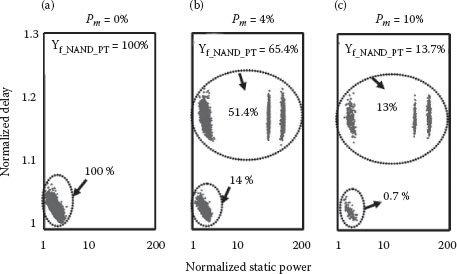
FIGURE 43.2 Monte Carlo simulation for a Parallel Tube (PT) NAND gate with Ntug = 48, showing normalized delay vs. static power for (a) absence of metallic tubes − Pm = 0%, (b) Pm = 4% metallic tubes, and (c) Pm = 10% metallic tubes with the delay constraint of 1.3× and the static power constraint of 200×. (R. Ashraf et al., Analysis of yield improvement techniques for CNFET-based logic gates, 2011 11th IEEE Conference on Nanotechnology (IEEE-NANO), August 15–18, pp. 724–729. © (2011) IEEE. With permission.)
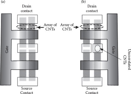
FIGURE 43.3 Tube configurations for (a) Transistor Stacking (TrS) and (b) Tube Stacking (TuS) CNFET. Both the configurations have the same number of channels to preserve the iso-input capacitance. (R. Ashraf et al., Analysis of yield improvement techniques for CNFET-based logic gates, 2011 11th IEEE Conference on Nanotechnology (IEEE-NANO), August 15–18, pp. 724–729. © (2011) IEEE. With permission)
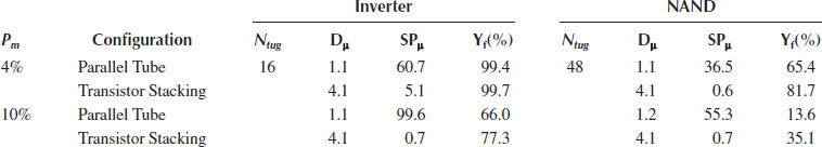
Table 43.1 summarizes the normalized mean delay, static power, and yield results generated by Monte Carlo simulations for an inverter and a two-input NAND gate with different transistor configurations. The percentage of metallic tubes, Pm, is assumed to be 4% and 10%. From the table, it can be observed that circuit-level techniques can be used to obtain acceptable functional yield if the percentage of metallic tubes is less than 5%. When the percentage of metallic tubes is relatively small below 5%, hybrid CNFET circuits built with mixtures of PT and TrS transistors achieve an acceptable yield.
When the percentage of metallic tubes is larger than 5%, the proposed circuit-level techniques are not sufficient. Extra processing steps to remove the metallic tubes are necessary. Both SCE and VMR techniques have trade-offs, as the removal process is not perfect and removes semiconducting tubes in addition to removing unwanted metallic tubes. Therefore, stochastic removal of tubes results in a large variation in the performance of CNFET-based gates, and in the worst case, it can create open-circuit gates. We have developed a Monte Carlo simulation engine to estimate the impact of the removal of tubes from driving gates on the performance and power of CNFET-based logic circuits.
In the analysis presented in Ref. [37], the authors assumed the fanout of the logic gates to be constant. However, this scenario is only applicable while driving the internal or external interconnect buses. In most other cases, gates will be driving other gates through local interconnects, and tubes removed from both the driving gates and fanout gates will impact the performance of the gates. If we consider the fanout to be constant, then it will result in the underestimation of the functional yield of logic gates. Therefore, in this chapter, we also discuss the effect of gate fanout on the functional yield of logic gates. It will be shown that fanout influence is especially important when extra processing steps are used to remove the finite numbers of tubes.
It has been shown previously that when metallic tubes are present, the use of highly uncorrelated (different) tubes among different transistors reduces the probability of an ohmic short, and increases the functional yield of logic gates. Now, if the extra processing steps such as SCE and VMR are used to remove the metallic tubes, the Monte Carlo results show that either of these techniques removes more than 99.9% of metallic tubes. The trade-off of using these removal techniques is large performance variation due to removal of the metallic tubes and also due to a side effect of undesired removal of semiconducting tubes. It is observed that when the tubes are removed, the use of highly uncorrelated tubes (different tubes) among different CNFETs results in a large variation in performance, and hence low functional yield. On the other hand, when the tube removal process removes almost all the metallic tubes, then use of highly correlated tubes results in less variation in performance and higher functional yields of CNFET-based gates. Therefore, when a large fraction of tubes needs to be removed, we expect transistors to be implemented with highly correlated tubes.
TABLE 43.1
Normalized Mean Delay, Normalized Static Power and Yield Comparisons for Inverter and 2-Input NAND Gate When Percentage of Metallic Tubes is 4% and 10%
Source: R. Ashraf et al., Analysis of yield improvement techniques for CNFET-based logic gates, 2011 11th IEEE Conference on Nanotechnology (IEEE-NANO), 15–18 August, pp. 724–729. © (2011) IEEE. With permission.
Note: Ntug is the number of tubes in the gate.
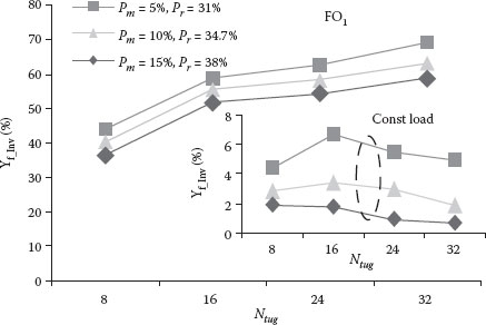
FIGURE 43.4 Summary of Monte Carlo yield simulation for inverters with a delay constraint of 1.3×, and a static power constraint of 10×. The yield is shown as a function of Ntug, Pm and Pr assuming a fanout of one (FO1) and when tubes are removed from both the driving and fanout gates (realistic scenario). The inset graph shows the MC yield simulation for inverters with the same delay and static power constraints and with the constant load. (R. Ashraf et al., Analysis of yield improvement techniques for CNFET-based logic gates, 2011 11th IEEE Conference on Nanotechnology (IEEE-NANO), August 15–18, pp. 724–729. © (2011) IEEE. With permission.)
Figure 43.4 shows a summary of the Monte Carlo yield simulation for inverters (with a delay constraint of 1.3 times and a static power constraint of 10 times) as a function of the number of tubes in the gate (Ntug), the percentage of metallic tubes (Pm) prior to the application of the tube removal process, and the percentage of metallic and semiconducting tubes removed (Pr). We consider the fanout of one, FO1, and assume that tubes are removed from both the driving gate and the fanout (realistic scenario as discussed in the previous paragraph). A sample size (n) of 10,000 gates was used for all Monte Carlo simulations. The inset graph in Figure 43.4 shows the Monte Carlo yield simulated for inverters when no tubes are removed from the fanout gates. Please observe that extremely low yields are obtained when we consider the fanout to be constant.
From the data discussion in the previous paragraph, it can be concluded that the removal of tubes creates two main problems: (1) open-circuit transistors/gates when all tubes are removed from a transistor and (2) low functional yields because of the finite number of tubes removed from the drive and fanout gates. To design robust circuits when finite numbers of tubes are removed from the gates by extra processing steps, we propose tube-level redundancy (TLR) to reduce the probability of open-circuit gates and to improve a functional yield of logic gates.
Our first objective is to find the minimum number of tubes (Nturmin) required in a transistor prior to the tube removal process for less than a 0.001% probability of open-circuit CNFETs being created after the tube removal step. Nturmin can be calculated as shown in Equation 43.4.
(43.4) |
Table 43.2 shows the Nturmin required for a negligible probability of open-circuit transistors for different percentages of metallic tubes. Numbers in Table 43.2 are calculated by assuming that the SCE technique is applied to remove metallic tubes and the cutoff diameters for metallic and semiconducting tubes are DCS = 1.4 nm and DCM = 2 nm, respectively. The same methodology can also be applied to the VMR technique.
TABLE 43.2
Minimum Number of CNTs Required in a CNFET to Produce 0.001% Probability of Open Circuit Transistors
![]()
Source: R. Ashraf et al., Analysis of yield improvement techniques for CNFET-based logic gates, 2011 11th IEEE Conference on Nanotechnology (IEEE-NANO), August 15–18, pp. 724–729. © (2011) IEEE. With permission.
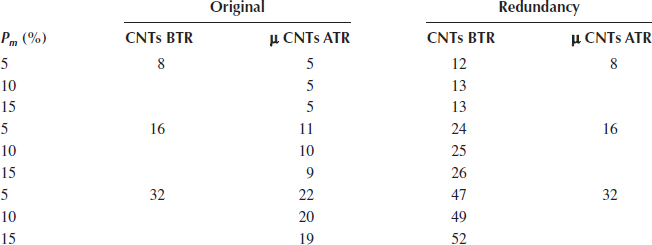
An efficient TLR technique that allows us to obtain acceptable levels of yield without sacrificing too much area and power is proposed in this chapter. It is based on adding the redundant tubes with the objective of obtaining the same mean number of tubes in the CNFET after tube removal as are required by the design prior to the tube removal process. Table 43.3 shows the efficient redundancy estimation technique to increase the functional yield of gates (when finite numbers of tubes are removed) with a minimal impact on the area and energy. For example, as can be noticed in Table 43.3, if for Pm = 10% the number of tubes required in a CNFET, prior to tube removal, is 8, then after the tube removal process the mean number of tubes remaining is 5. However, if 13 tubes are present in the CNFET prior to the tube removal process, then the mean number of tubes after the tube removal process is 8 and is equal to the required number of tubes.
Figure 43.5 shows the Monte Carlo simulation results for NAND gates with the number of tubes, Ntug = 48. Figure 43.5b shows the functional yield results for Pm = 10% and Pr = 35% of the tubes removed by the tube removal process. In such a case, only 66% of the gates are functional. By the redundancy-based methodology explained in the previous paragraph, 72 tubes, Ntugr = 72, are required in the gate to yield the mean number of 48 tubes after the tube removal process. This added redundancy of 50% increased the functional yield from 66% to 74%. By using this redundancy technique, the increase in area is 50% and the mean energy of the gate is increased by 17%.
TABLE 43.3
Original CNTs in a CNFET before Tube Removal (BTR) and after Tube Removal (ATR) for Different Percentage of Metallic Tubes
Source: R. Ashraf et al., Analysis of yield improvement techniques for CNFET-based logic gates, 2011 11th IEEE Conference on Nanotechnology (IEEE-NANO), August 15–18, pp. 724–729. © (2011) IEEE. With permission.
Note: Number of CNTs required in a CNFET BTR that will produce the same mean CNTs in a CNFET after tube removal as are initially required by design BTR.
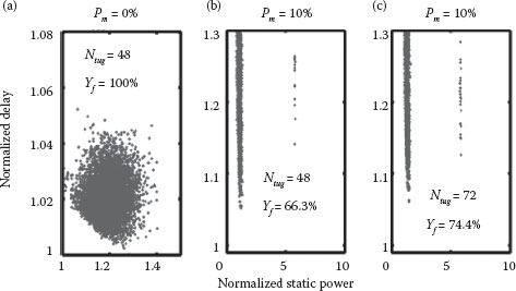
FIGURE 43.5 Monte Carlo simulation for NAND gates showing normalized delay vs. static power for (a) Ntug = 48, 0% metallic and no tube removal, (b) Ntug = 48, 10% metallic and 35% tubes are removed, (c) Ntugr = 72, 10% metallic and 35% tubes are removed. The yields are 100%, 66%, and 74%, respectively. (R. Ashraf et al., Analysis of yield improvement techniques for CNFET-based logic gates, 2011 11th IEEE Conference on Nanotechnology (IEEE-NANO), August 15–18, pp. 724–729. © (2011) IEEE. With permission.)
Notice that the yield of 72% is still considered low, but it is anticipated that it would improve in large circuits, where we should consider multiple gates that are cascaded to form multistage logic networks. Depending on the logic depth of a logic network, a certain amount of statistical averaging in delay variation is expected and observed. Thus, less than 100% yield at the gate level might be sufficient to obtain an acceptable yield at the system level.
In this chapter, we explored the potential of CNTs to be used as a channel material in the future field-effect transistors for application in integrated circuits. We also showed that despite the detrimental impact of the unwanted metallic tubes on the performance, power, and yield of CNFET-based circuits, possible solutions to build robust CNFET-based circuits with an acceptable performance and a reasonable functional yield can be found. For small percentages of metallic tubes, circuit-level techniques such as TrS and TuS configurations can be used to build robust CNT-based circuits. For larger percentages of metallic tubes, robust CNT-based circuits, with acceptable functional yield, can be designed using the proposed TLR approach and fabrication by using extra processing techniques for metallic tube removal.
1. P. L. McEuen, M. S. Fuhrer, and P. Hongkun, Single-walled carbon nanotube electronics, IEEE Trans. Nanotechnol., 1(1), 78–85, Mar. 2002.
2. D. S. Bethune, C. H. Klang, M. S. de Vries, G. Gorman, R. Savoy, J. Vazquez, and R. Beyers, Cobaltcatalysed growth of carbon nanotubes with single-atomic-layer walls, Nature, 363(6430), 605–607, Jun. 1993.
3. S. Iijima and T. Ichihashi, Single-shell carbon nanotubes of 1-nm diameter, Nature, 363(6430), 603–605, Jun. 1993.
4. A. Raychowdhury, A. Keshavarzi, J. Kurtin, V. De, and K. Roy, Carbon Nanotube field-effect transistors for high-performance digital circuits-DC analysis and modeling toward optimum transistor structure, IEEE Trans. Electron Devices, 53(11), 2711–2717, Nov. 2006.
5. A. Javey, J. Guo, D. B. Farmer, Q. Wang, E. Yenilmez, R. G. Gordon, M. Lundstrom, and H. Dai, Self-aligned ballistic molecular transistors and electrically parallel nanotube arrays, Nano Lett., 4(7), 1319–1322, Jul. 2004.
6. Z. Yao, C. L. Kane, and C. Dekker, High-field electrical transport in single-wall carbon nanotubes, Phys. Rev. Lett., 84(13), 2941–2944, Mar. 2000.
7. T. Durkop, S. A. Getty, E. Cobas, and M. S. Fuhrer, Extraordinary mobility in semiconducting carbon nanotubes, Nano Lett., 4(1), 35–39, 2004.
8. A. Javey, J. Guo, D. B. Farmer, Q. Wang, D. Wang, R. G. Gordon, M. Lundstrom, and H. Dai, Carbon nanotube field-effect transistors with integrated ohmic contacts and high-k gate dielectrics, Nano Lett., 4(3), 447–450, Mar. 2004.
9. A. Javey, H. Kim, M. Brink, Q. Wang, A. Ural, J. Guo, P. McIntyre, P. McEuen, M. Lundstrom, and H. Dai, High-K dielectrics for advanced carbon-nanotube transistors and logic gates, Nat. Mater., 1(4), 241–246, Dec. 2002.
10. J. Guo, S. Datta, M. Lundstrom, M. Brink, P. McEuen, A. Javey, H. Dai, H. Kim, and P. McIntyre, Assessment of silicon MOS and carbon nanotube FET performance limits using a general theory of Ballistic transistors, in Proc. Int. Electron Devices Meet., 2002, pp. 711–714.
11. J. Guo, A. Javey, H. Dai, and M. Lundstrom, Performance analysis and design optimization of near Ballistic carbon nanotube field-effect transistors, in Proc. Int. Electron Devices Meet., 2004, pp. 703–706.
12. B. Q. Wei, R. Vajtai, and P. M. Ajayan, Reliability and current carrying capacity of carbon nanotubes, Appl. Phys. Lett., 79(8), 1172–1174, 2001.
13. A. Nieuwoudt and Y. Massoud, Evaluating the impact of resistance in carbon nanotube bundles for VLSI interconnect using diameter-dependent modeling techniques, IEEE Trans. Electron Devices, 53(10), 2460–2466, 2006.
14. M. Budnik, A. Raychowdhury, A. Bansal, and K. Roy, A high density, carbon nanotube capacitor for decoupling applications, in Proc. ACM/IEEE Design Automat. Conf., 2006, pp. 935–938.
15. A. Nieuwoudt and Y. Massoud, High density integrated capacitors using multi-walled carbon nanotubes, in IEEE Conf. Nanotechnol., 2007, pp. 387–390.
16. K. Tsubaki, H. Shioya, J. Ono, Y. Nakajima, T. Hanajiri, and H. Yamaguchi, Large magnetic field induced by carbon nanotube current proposal of carbon nanotube inductors, in Device Res. Conf. Digest, 2005, vol. 1, pp. 119–120.
17. K. Tsubaki, Y. Nakajima, T. Hanajiri, and H. Yamaguchi, Proposal of carbon nanotube inductors, J. Phys. Conf. Ser., 38, 49–52, May 2006.
18. A. Nieuwoudt and Y. Massoud, Carbon nanotube bundle-based low loss integrated inductors, in IEEE Conf. Nanotechnol., 2007, pp. 714–718.
19. N. Chimot, V. Derycke, M. F. Goffman, J. P. Bourgoin, H. Happy, and G. Dambrine, Gigahertz frequency flexible carbon nanotube transistors, Appl. Phys. Lett., 91(15), 153111–153113, Oct. 2007.
20. Q. Cao, H. Kim, N. Pimparkar, J. P. Kulkarni, C. Wang, M. Shim, K. Roy, M. A. Alam, and J. A. Rogers, Medium-scale carbon nanotube thin-film integrated circuits on flexible plastic substrates, Nature, 454(7203), 495–500, Jul. 2008.
21. J. Deng, N. Patil, K. Ryu, A. Badmaev, C. Zhou, S. Mitra, and H.-S. P. Wong, Carbon nanotube transistor circuits: Circuit-level performance benchmarking and design options for living with imperfections, in Proc. Int. Solid State Circuits Conf., 2007, pp. 70–588.
22. C. Kocabas, M. Shim, and J. A. Rogers, Spatially selective guided growth of high-coverage arrays and random networks of single-walled carbon nanotubes and their integration into electronic devices, J. Am. Chem. Soc., 128(14), 4540–4541, Apr. 2006.
23. S. J. Kang, C. Kocabas, T. Ozel, M. Shim, N. Pimparkar, M. A. Alam, S. V. Rotkin, and J. A. Rogers, High-performance electronics using dense, perfectly aligned arrays of single-walled carbon nanotubes, Nat. Nanotechnol., 2(4), 230–236, Apr. 2007.
24. Y. Li, D. Mann, M. Rolandi, W. Kim, A. Ural, S. Hung, A. Javey et al., Preferential growth of semiconducting single-walled carbon nanotubes by a plasma enhanced CVD method, Nano Lett., 4(2), 317–321, 2004.
25. L. Qu, F. Du, and L. Dai, Preferential syntheses of semiconducting vertically aligned single-walled carbon nanotubes for direct use in FETs, Nano Lett., 8(9), 2682–2687, Sep. 2008.
26. Y. C. Tseng, K. Phoa, D. Carlton, and J. Bokor, Effect of diameter variation in a large set of carbon nanotube transistors, Nano Lett., 6(7), 1364–1368, Jul. 2006.
27. P. Avouris, J. Appenzeller, R. Martel, and S. J. Wind, Carbon nanotube electronics, Proc. IEEE, 91(11), 1772–1783, Nov. 2003.
28. A. Raychowdhury, V. K. De, J. Kurtin, S. Y. Borkar, K. Roy, and A. Keshavarzi, Variation tolerance in a multichannel carbon-nanotube transistor for high-speed digital circuits, IEEE Trans. Electron Devices, 56(3), 383–392, Mar. 2009.
29. N. Patil, J. Deng, H.-S. P. Wong, and S. Mitra, Automated design of Misaligned-carbon-nanotube-immune circuits, in Proc. ACM/IEEE Design Automat. Conf., San Diego, CA, 2007, pp. 958–961.
30. S. Bobba, J. Zhang, A. Pullini, D. Atienza, H.-S.P. Wong, and G. De Micheli, Design of compact imperfection-immune CNFET layouts for standard-cell-based logic synthesis, in Proc. Design, Automat. Test Eur., 2009.
31. http://www.itrs.net/Links/2009ITRS/Home2009.htm/, Emerging Research Devices.
32. J. Deng and H.-S. P. Wong, A circuit-compatible SPICE model for enhancement mode carbon nanotube field effect transistors, in Int. Conf. Simulation Semiconductor Processes Devices, SISPAD, 2006, pp. 166–169.
33. I. Amlani, J. Lewis, K. Lee, R. Zhang, J. Deng, and H.-S. P. Wong, First demonstration of AC gain from a single-walled carbon nanotube common-source amplifier, in Proc. Int. Electron Devices Meet, 2006, pp. 1–4.
34. W. Zhao and Y. Cao, New generation of predictive technology model for sub-45 nm design exploration, in IEEE Trans. Electron Devices, 2006, pp. 585–590.
35. G. Zhang, P. Qi, X. Wang, Y. Lu, X. Li, R. Tu, S. Bangsaruntip, D. Mann, L. Zhang, and H. Dai, Selective etching of metallic carbon nanotubes by gas-phase reaction, Science, 314(5801), 974–977, Nov. 2006.
36. N. Patil, A. Lin, J. Zhang, Hai Wei, K. Anderson, H.-S. P. Wong, and S. Mitra, VMR: VLSI-compatible metallic carbon nanotube removal for imperfection-immune cascaded multi-stage digital logic circuits using carbon nanotube FETs, in Proc. Int. Electron Devices Meet, Baltimore, MD, USA, 2009, pp. 1–4.
37. R. Ashraf, N. Rajeev, C. Malgorzata, and N. Siva G., Yield enhancement by tube redundancy in CNFET-based circuits, in IEEE Int. Conf. Electron. Circuits Syst., 2010.
38. R. Ashraf, M. Chrzanowska-Jeske, and S.G. Narendra, Analysis of yield improvement techniques for CNFET-based logic gates, 2011 11th IEEE Conference on Nanotechnology (IEEE-NANO), August 15–18, 2011, pp. 724–729.