
Nonvolatile Logic-in-Memory Architecture An Integration between Nanomagnetic Logic and Magnetoresistive RAM |
|
CONTENTS
60.2 Operating Principles of Logic Inside the Architecture
60.3 Specifications of the Logic-in-Memory Architecture
60.3.1 Salient Features of the Architecture
60.3.2 Cell Types in the Architecture
60.4 Basic Operations for Logic Computation
60.5 Performance Analysis of the Architecture
60.5.1 Comparison with Existing Logic-in-Memory Architectures
The use of magnetism for data storage dates back to the early days of computers when magnetic core memories were popular. Magnetic core memories were built of tiny magnetic toroids (commonly called cores). The memories exhibited hysteresis characteristics that enabled them to store 1 and 0 along two stable states of magnetization [1, 2 and 3]. The magnetic core memories were rewritable, non-volatile, and radiation hard. However, they were bulky and slow. On the other hand, the semiconductor memories, static RAM (SRAM), and dynamic RAM (DRAM) that replaced the magnetic core memories are fast, rewritable, and compact. However, they are volatile [4] and require constant voltage supply. In addition, the DRAM requires periodic refreshing to retain data. With the introduction of semiconductor memories, both data storage and logic computation became electronic in nature. But the storage and computation continued to remain in separate regions inside a computer. Any logic operations inside the central processing unit (CPU) required data to be fetched from memory, which in turn posed a bottleneck to high-speed computing. To resolve this issue, researchers started focusing on ways to embed logic and memory into a single plane and various logic-in-memory architectures were developed. Various devices were also studied as potential candidates for logic-in-memory applications. Further discussion on these previous studies in logic-in-memory is scheduled for Section 60.5.1.
The latest trend in data storage has moved back to the magnetic domain. The modern magnetoresistive memories, called magnetoresistive RAMs (MRAMs), use magnetization to store binary information. MRAMs are nonvolatile and radiation hard, and can sustain high temperatures. They are built using magnetic tunnel junctions (MTJs) that have correlated electric and magnetic properties. MTJs are primarily composed of two single-domain ferromagnetic layers that are vertically stacked and separated by a nonmagnetic barrier layer. One of the layers has a fixed magnetization while the other is free to rotate in a plane. The layers are called the fixed and free layers respectively, in accordance with their magnetic properties. In MTJs, a logic 1 or a logic 0 is represented with the help of relative magnetization between the free and fixed layers (see Figure 60.1). The 1 or 0 in an MTJ is written with the help of external magnetic fields or a spin-transfer torque (STT) current. In Toggle MRAMs [5], external magnetic fields generated by current-carrying wires are used for writing. In the more recent STT-MRAMs, STT current is used to write 1 or 0 into MTJs. The STT current-induced writing is low power in comparison to external field-driven writing and will be the only writing mechanism considered in this chapter. The value once written into MTJ remains stored through magnetic remanence and there is no leakage of magnetism with time. This makes the MRAMs truly nonvolatile memories.
Apart from STT current-induced magnetization switching, the electrical resistance of MTJs is also closely interlinked to their magnetic state. The electrical resistances (R0 and R1) of the logic 0 and 1 states of MTJs are well distinguished from each other and their difference is used to define the tunnel magnetoresistance (TMR) of MTJs (see Equation 60.1).
(60.1) |
The electrical resistance of MTJs is used to read the bits in MRAM. MTJs are also integrable to CMOS. In MRAM, every single MTJ is integrated to an NMOS access transistor [6] (see Figure 60.2). The combined MTJ-CMOS unit is then used to define a bit in memory. In MRAM, three layers of metal are used to define the source, bit, and word lines. The bit and source lines are used to apply the desired potential across MTJs, whereas the word line is used to select the access transistors of the MTJs. Together, the three metal lines are used to select a bit in memory for read or write.
The placement of MTJs inside MRAM is like a regular 2D array with a separation d between any two MTJs (see Figure 60.3). The bit and source lines are parallel to the rows of MTJs while the word lines are parallel to the columns of MTJs. For example, to select a bit in the (i,j)th location in MRAM, i and j being the row and column numbers, respectively, the jth word line is first raised high. An appropriate potential is next applied across the ith bit and source line pair. The separation d determines the density of the memory. The lower the d, the denser is the memory. However, lowering d beyond a limit dm increases the tendency of the interaction between the free layers of MTJs. This interaction is undesirable in memory where the bits are independent of each other. The interaction would however play a decisive role if used in logic. Designed at this junction of logic and memory behavior of MTJs is the logic-in-memory architecture [7] that is described in this chapter.
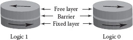
FIGURE 60.1 Logic states in MRAM.
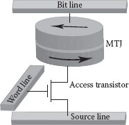
FIGURE 60.2 MTJ with an access transistor. (From G. Sun et al., A novel architecture of the 3D stacked MRAM l2 cache for cmps, in IEEE 15th International Symposium on High Performance Computer Architecture, 2009, HPCA 2009, pp. 239–249, Feb. 2009.)
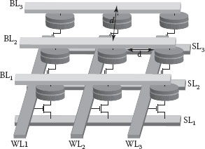
FIGURE 60.3 MRAM layout.
The main motivation behind the logic-in-memory design has remained the same: to reduce data traffic between memory and the CPU. The goal of the architecture described in this chapter is to compute some simplistic logic within memory while performing the complex operations in the CPU. The architecture is regular like MRAM in its MTJ placements. However, it remains unique from MRAM in its CMOS integration and layout of metal lines. In this architecture, the clock signal acts as a classifier between logic and memory operations. With a clock, the MTJs interact among their free layers and compute logic. Without a clock, the MTJs retain their contents and behave as memory. In the next few sections, we will closely focus on the operating principles and the key specifications of the architecture.
60.2 OPERATING PRINCIPLES OF LOGIC INSIDE THE ARCHITECTURE
The working principles of nanomagnetic logic (NML) [8] govern the logic execution inside the architecture. In NML, single-domain single-layer nanomagnets are used to build logic. The magnetizations in the nanomagnets are used to represent 1 and 0 in logic (see Figure 60.4). Both the logic states are along the easy axes of the nanomagnets, which are also the energy minimum states for the nanomagnets (see Figure 60.5). The magnetic interaction between the nanomagnets, together with a clocking signal, is used to compute logic. External magnetic fields generated by current carrying wires are used as a clock in NML [9, 10 and 11]. When clocked, the magnetization in the nanomagnets orient along the saddle points or the energy maximum state (see Figure 60.6). This state is unstable and once the clock is released, the nanomagnets settle in accordance with the net magnetic fields acting on them. The magnetic interaction or coupling between the nanomagnets are of two different types: ferromagnetic and antiferromagnetic. When ferromagnetically coupled, the nanomagnets have the same magnetization. When antiferromagnetically coupled, the nanomagnets have opposite magnetizations (see Figure 60.7).
FIGURE 60.4 Bit representation in single-layer nanomagnets.
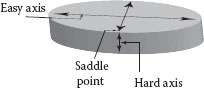
FIGURE 60.5 Easy axis, hard axis, and saddle point in a nanomagnet.
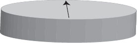
FIGURE 60.6 A clocked single-layer nanomagnet in NML.
In this architecture, the logic computation takes place in the free layers of MTJs. The free layers behave like the single-domain nanomagnets in NML. The dipolar magnetic coupling between the free layers of MTJs takes responsibility for logic computation. Two ferromagnetically coupled MTJs will have their free layers magnetized in the same direction while two antiferromagnetically coupled MTJs will have their free layers magnetized in opposite directions (see Figure 60.8). However, like NML, these couplings play an active role in logic computation only when they are accompanied by a suitable clock signal.
Like NML [12], the clock in this architecture has dual functions: (i) to synchronize events during the course of logic execution and (ii) to help the magnetization of the free layer overcome the potential barrier separating the logic 0 from the logic 1 state and vice versa. When clocked, the MTJs are in an energy maximum state [13]. When the clock is released, the MTJs settle into one of their energy minimum states (i.e., logic 0 or logic 1), depending on the resultant coupling force acting from neighboring MTJs. However, the implementation of the clock in this architecture is uniquely different from that of NML. It uses a train of STT current pulses to clock the MTJs [14]. The STT current-driven clock used in this architecture is low-power compared to the external field-driven clock practiced in NML. The STT clock also requires the fixed layers of MTJs to have a 45° magnetization polarization (see bottom layer in Figure 60.8). The magnetization of the free layer of MTJs remains in plane. The other two major operations in logic are writing inputs and reading outputs. In this architecture, both the operations are carried out electrically using current. Further details of the clocking, writing, and reading techniques followed in the architecture are discussed under Section 60.4.
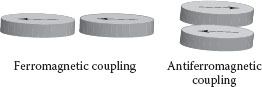
FIGURE 60.7 Dipolar magnetic coupling between single-layer nanomagnets.
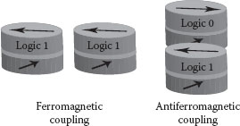
FIGURE 60.8 Dipolar magnetic coupling between free layers of MTJs.
60.3 SPECIFICATIONS OF THE LOGIC-IN-MEMORY ARCHITECTURE
A section of the architecture is shown in Figure 60.9. The MTJs rest above a CMOS plane that houses access transistors for selected MTJs in the architecture. Ideally, a designer would prefer to have an access transistor with every MTJ in the architecture to gain user control over every logic cell. However, certain technology constraints have prohibited this ideal integration between access transistors and MTJs in this architecture as we will discuss below.
For successful logic computation, MTJs need to be 20 nm apart [15]. The planar surface area chosen for this architecture is 100 × 50 nm2. The values are derived from the single-domain behavior of MTJs and stability at room temperature. On the other hand, the metal pitch of the CMOS technology to be used determines the minimum separation between the two access transistors. With the latest available 22 nm CMOS technology node, the metal pitch requirement for the layer 1 is 64 nm [16]. This is again the minimum metal pitch available from any present CMOS technology. This contention between the CMOS access transistor spacing and the MTJ spacing puts a restriction over CMOS integration with every MTJ in the architecture. The integration between CMOS and MTJs therefore needs to be optimized. As an optimum solution to this problem, in this architecture, an access transistor is integrated with every alternate MTJ that is located either in a column or in a row (see Figure 60.9). The outcome is that we now have two sets of MTJs in the architecture: one with an access transistor (Figure 60.9: X11, X13, X31, X33) and the other without an access transistor (Figure 60.9: X12, X21, X22, X23, X32). The rule of their placements in the architecture sets the salient features for the architecture [14].
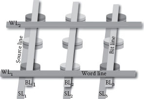
FIGURE 60.9 Regular placement of MTJs in the logic-in-memory architecture. Only the dark gray MTJs have an access transistor integrated underneath. For simplicity, access transistors are not shown in this figure.
60.3.1 SALIENT FEATURES OF the ARCHITECTURE
1. An access transistor for every 2 × 2 MTJ array: Figure 60.9 shows the integration of access transistors with MTJs in the architecture. All the access transistors in the architecture are NMOS without any exception.
2. A source and bit line for every row and a word line for every alternate column: A source and bit line pair, housed in metal layers 1 and 2, run parallel to the rows of cells in the architecture. The purpose of the source and bit lines in the architecture is to supply a suitable potential across MTJs during writing, clocking, and reading. The bit lines are always aligned with the row axes of the architecture. They are connected to the free layers of the MTJs through vias (see Figure 60.10). The connection between the source lines and MTJs vary depending on the presence or absence of access transistors. For MTJs without access transistors, the source lines are directly connected to the fixed layers of the MTJs through vias. For MTJs with access transistors, the source lines are connected to either the source or drain terminals of the access transistors. The second terminal (drain or source) of the access transistor then connects to the fixed layer of the MTJ, thereby completing the electrical path between the source and bit line through the MTJ (see Figures 60.10 and 60.11).
The word line is housed in metal layer 3 and runs orthogonal to the first two metal layers. The word line is used to connect the gates of access transistors that are all integrated to MTJs in a single column (see Figure 60.10). Since the access transistors are present with MTJs that lie in alternate columns, the word lines are also present along alternate columns of MTJs (see Figure 60.9). The metal pitch calculated from the layout (Figure 60.11) for the source, bit, and word lines are 70, 120, and 140 nm, respectively. The metal 1 pitch in 22 nm CMOS technology is 64 nm [16], while the metal 2 and 3 pitches are each >64 nm. The architecture therefore satisfies 22 nm CMOS pitch requirements.
60.3.2 CELL TYPES IN the ARCHITECTURE
Depending on their assigned functions inside a logic, the MTJs (alternately addressed as cells) in the architecture are classified into three broad categories:
1. Input cells: These cells only participate as inputs of logic. Only those MTJs that have access transistors are selected as input cells. During the entire course of the logic operation, these cells are written only once. Their values remain unchanged throughout the course of logic execution. These cells are therefore never clocked.
2. Output cells: The final output of logic is produced in these MTJs. Again, only those MTJs that have access transistors are selected. These cells participate in logic and are therefore always clocked. In addition, their contents are also read whenever the output of the logic needs to be known.
3. Logic cells: These cells form the body of the logic and are present in between the input and output cells. MTJs with and without access transistors belong to this group of cells. These cells are always clocked whenever logic is computed.
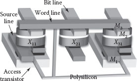
FIGURE 60.10 A column of MTJs inside the architecture. (J. Das, S.M. Alam, and S. Bhanja, Ultra-low power hybrid CMOS-magnetic logic architecture, IEEE Transactions on Circuits and Systems I: Regular Papers, 59(9), pp. 2008–2016 © (2012) IEEE.)
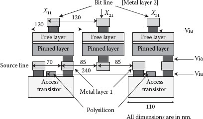
FIGURE 60.11 Cross section of the column of MTJs shown in Figure 60.10. (J. Das, S. M. Alam, and S. Bhanja, Low power CMOS-magnetic nano-logic with increased bit controllability, in 11th IEEE Conference on Nanotechnology IEEE-NANO, pp. 1261–1266 © (2012) IEEE.)
Figure 60.12 shows an example layout of a two-input AND gate built in this architecture. Inputs A and B are written into input cells X1 and X2. The result A ∙ B is produced in X3. The cell on the left of X3 has a fixed magnetization of 1. However, with the given architecture specifications, X3 cannot have an access transistor; neither can any MTJ (X4 and X5) in its row. Therefore, none of X3, X4, and X5 can qualify as an output cell. X3 now becomes a logic cell and its value needs to be propagated to the nearest MTJ that fulfills the criteria of an output cell. An MTJ in the row of X1 or X2 can be a possible candidate. A second condition of the output cell is that it should be located at least one cell apart from the input cells X1 or X2. This ensures that the inputs do not have any direct influence on the output. X6 fulfills the requirement for an output cell. X4 and X5 are then used to propagate the value from X3 to X6. X4 and X5 also become logic cells.
60.4 BASIC OPERATIONS FOR LOGIC COMPUTATION
The three basic operations to be carried out in any logic are
1. Writing inputs
2. Clocking cells
3. Reading outputs
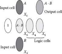
FIGURE 60.12 Two-input AND.
In the architecture described in this chapter, all these three operations are current driven and vary in magnitude and the duration of the current. We will now focus on how each of these operations is carried out in the architecture.
Every input cell in the architecture has an access transistor. Whenever an input, 1 or 0, needs to be written into an input cell, its access transistor needs to be turned on to complete the path for the current through the MTJ. By applying an active high voltage on the word line corresponding to the column of the input cell, its access transistor is turned on. Depending on the input value to be written, the current direction and magnitude through the MTJ also change. For example, to write logic 1, current needs to flow from the bit to the source line. Current from a source to a bit line is required to write a logic 0. During writing 1 and 0, the terminals of the access transistor switch roles between the source and the drain, depending on the direction of the current. The typical current magnitudes calculated for writing 1 and 0 into the input cells are 280 and 216 µA, respectively, with approximate durations of 20 ps [17]. Once all the inputs are written, the next step in logic is to compute. The most important operation during logic computation is clocking, which is discussed in the next section.
As mentioned in Section 60.2, the logic cells are clocked using a train of STT current pulses. Whenever an MTJ is clocked, the magnetization of its free layer is held in a stationary state along the direction of the saddle points (see Figure 60.13, Phase III). To gain a deeper insight into the STT clock, we need to focus on the modified Landau–Lifshitz–Gilbert (LLG) equation (Equation 60.2) that describes the magnetodynamics behavior of an MTJ free layer with STT current.
(60.2) |
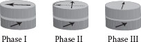
FIGURE 60.13 Different phases of STT-clocking in MTJ.
In the above equation, m and ep are unit vectors along the magnetization of the free and fixed layers, respectively. Ms is the saturation magnetization of the free layer. heff is the effective normalized magnetization field on the free layer that is a sum of the crystalline and shape anisotropic fields, the demagnetization field, the exchange field, and the coupling from the underlying fixed layer. γ is the gyromagnetic ratio and α is the damping coefficient. Parameters G and Jp are defined in Equation 60.3. The other parameters in Equation 60.3 are P—the spin-polarizing factor; —the unit vectors along the global spin orientation of the fixed and free layers of MTJ; e—the electron charge; ħ—the reduced Planck’s constant; and d—the thickness of the free layer. Je is the applied STT current. When an MTJ is STT clocked, the current magnitude |Je| (Equation 60.4, [13]) cancels the magnetic precession of the free layer, reducing the left-hand side of Equation 60.2 to zero. In Equation 60.4, Hd is the coupling between the fixed and the free layers. It is also worth mentioning here that the MTJ fixed layer polarization of 45° that is mentioned in Section 60.2 is imposed by this STT clocking.
(60.3) |
(60.4) |
The STT clocking in the logic takes place in three phases: (i) an initial writing of 1 into the MTJs, (ii) an intermediate half precession sweep to the saddle point, and (iii) the final stationary magnetization state along the saddle point (see Figure 60.13). Each of the three phases requires three different currents. The current magnitudes for the first and second phases remain the same as the STT writing of logic 1 and 0 into the MTJs. The current estimate for the final phase is 170 µA [13].
Once a logic is computed, its output needs to be read. The TMR of MTJs described by Equation 60.1 provides an electrical base for determining the logic output. By reading the electrical resistance of an output cell, its values can be determined. In our logic-in-memory architecture, the output is determined through a differential read approach using complementary output values [14]. In logic, there exists a dependency among bits. The dependency between two adjacent logic bits Xi−1 and Xi in a row can be probabilistically expressed in the ideal case as p(Xi = 1|Xi−1 = 0) = p(Xi = 0|Xi−1 = 1) = 1. Here, Xi is influenced by only its left neighbor Xi−1 through antiferromagnetic coupling. The differential read discussed in this section is developed on this property of logic. Figure 60.14 shows the read circuit. Sa and are the complementary output cells from the logic that are placed in the two arms of the sense amplifier. M1a and M2a are their respective access transistors. (At this point, ignore cells Sb, and their access transistors M1b, M2b in Figure 60.14. Their functions will be explained later in the section.)
Brief description of the circuit operation: The read circuit operates in two consecutive phases: the precharge phase followed by the sense phase. In the precharge phase, signals ϕ2 and ϕ3 are pulled low to (i) turn off transistors M3 and M4 and (ii) simultaneously precharge nodes X and Y to VDD. The potential at nodes X and Y are equalized by setting Eq to an active high potential. In the sense phase, a low voltage signal Vread is applied on ϕ2. This is used to provide an equal bias on the output MTJs Sa and . Simultaneously, ϕ3 is raised high and Eq is pulled low to turn off transistors M7, M8, and M9. The difference in electrical resistances between Sa and starts to develop a differential voltage across X and Y that is finally read by the comparator. A high or low at the comparator output decides in favor of Sa = 1 or Sa = 0.
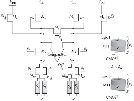
FIGURE 60.14 Nondestructive variability tolerant differential read for logic-in-memory architecture. (J. Das, S.M. Alam, and S. Bhanja, Ultra-low power hybrid CMOS-magnetic logic architecture, IEEE Transactions on Circuits and Systems I: Regular Papers, 59(9), pp. 2008–2016. © (2012) IEEE.)
The read operation described above is low-power. It requires an average current of 31 µA to read a 0 and 28 µA to read a 1 from an output cell. It is nondestructive and provides a near 50% improvement in sense margin over the conventional MRAM read using reference values.
The bit dependency in logic also produces equal values among alternate cells in a row of logic. This inherent property of logic is used to further modify the read circuit to make it variability tolerant. Instead of comparing a single bit (Sa) against its complement , the sense amplifier now compares a pair of similar-valued bits (Sa, Sb) against their complements (see Figure 60.14). Bit dependency in logic makes these bits readily available for read. Apart from an increased tolerance to variability, the modification also increases the sense margin of the read circuit [18].
60.5 PERFORMANCE ANALYSIS OF THE ARCHITECTURE
Before we conclude our discussion on our logic-in-memory architecture, we would present before our readers two brief comparative studies with our present architecture: (a) comparison with operating principles of existing logic-in-memory architectures and (b) comparison of logic principles and their performance with traditional NML.
60.5.1 COMPARISON WITH EXISTING LOGIC-in-MEMORY ARCHITECTURES
The motivation behind all logic-in-memory architectures is to reduce the communication bottleneck between memory and CPU. Research has evolved over different devices for logic-in-memory architectures. One of the early works in logic-in-memory uses cellular arrays, a two-dimensional iterative configuration of identical cells that contain both logic and memory elements [19]. The logic and memory elements are both fabricated in CMOS technology. Each cell in the array is a combination of gates and flip-flops. Computation and storage location inside a cell, however, remain distinct, thereby increasing the hardware complexity and associated costs. Additional costs involve invoking special design techniques to map a logic design onto the cellular arrays [20]. The multiple-valued floating gate MOS transistor used for logic-in-memory VLSI [21] compiles storage and switching functions in a multiple-valued input and binary output combinational logic. In this design concept, the stored data are distributed in word-parallel and digit-parallel manners throughout the logic plane. A third logic-in-memory design uses ferroelectric capacitors [22]. Ferroelectric capacitors in combination with MOS transistors are used to develop a complementary ferroelectriccapacitor (CFC) logic gate with both logic and memory functions. However, within a gate, the logic and memory elements still remain separate. A stored input vector is distributed into CFC logic gates and a series parallel combination of CFC logic gates is used to realize any logic. The final logic-in-memory architecture that we would discuss here is TMR based. In the TMR-based logic-in-memory [23], a literal generator, a wired sum circuit, and a threshold detector are combined together. The TMR-based devices are distributed in a logic circuit plane along with CMOS transistors. The devices are used for storing primary inputs, in particular those inputs that change least frequently. The resistances of these devices are then used to compute logic.
From the above, we can observe the following trends in all of the previous logic-in-memory architectures:
• Embedding memory elements within the logic plane
• Selective storing of inputs from an entire logic operation
• Keeping the logic and memory elements separate inside a logic-in-memory cell
The principle of our logic-in-memory architecture is different from the above-mentioned trend. In our architecture, the logic elements themselves behave as memory. The clock acts as a classifier between their participation in logic and behavior as memory. The logic operations are carried to the memory plane to perform some simplistic operations within the memory. The more complex logic operations will however remain with the CPU. The entire operation is nonvolatile. Information from various stages of operation can be retrieved as and when required without reexecuting any logic. It is worth mentioning at this point about the zero standby power from our logic-in-memory design.
Table 60.1 compiles a comparison between logic operations in traditional NML and our logic-in-memory architecture. The following are evident from the table.
Logic built with multilayer STT-MTJs are more favorable in terms of
1. Overall power consumption, which is the sum of the power consumed from writing inputs, clocking cells, and reading outputs
2. User control over cells in the logic
3. CMOS compatibility
4. Electrical interface of input and output signals
Other benefits of the logic-in-memory architecture include provision for logic decomposition that significantly reduces the cell count and overall power consumption of the logic. Further details of it are available in Ref. [24] and are beyond the scope of this chapter. A layout constraint in NML that arises whenever a bit and its complement are required in a single column of cells can be solved in this architecture. This would further optimize the cell count and power in logic [25]. In this chapter, we have only considered Boolean logic computations using dipolar magnetic coupling. Non-Boolean computing using magnetic logic is also an active research area and is discussed in Chapter 62. One of its major applications is in computer vision.
TABLE 60.1
Comparison of Logic Behavior and Logic Performance between Traditional NML and Discussed Logic-in-Memory Architecture
Nanomagnetic Logic |
Logic-in-Memory Architecture |
|
Logic Characteristics |
||
Cell types |
Single layer nanomagnets |
Multilayer magnetic tunnel junctions [14] |
Cell dimensions and spacing |
100 × 50 nm2, 20 nm [26] |
100 × 50 nm2, 20 nm [15] |
Computation style |
Dipolar magnetic coupling: ferro and antiferro [8] |
Dipolar magnetic coupling: ferro and antiferro |
CMOS compatibility |
None |
Yes, access transistor with MTJs |
User control |
Restricted to entire rows and columns, not to individual cells |
Up to one in 2 × 2 cells [14] |
Signal Types and Operating Styles |
||
Inputs |
Magnetic, external fields or through explicit neighbor magnets [27] |
Electric, STT current [14] |
Clock |
Magnetic, external fields [28] |
Electric, STT current [13] |
Outputs |
Magnetic, magnetic force microscopy [27] |
Electric, TMR based [14] |
Current and Timing |
||
Input current (writing 1) |
280 µA, 20 ps [14] |
|
Input current (writing 0) |
216 µA, 20 ps [14] |
|
Clocking current |
2.29 mA, 3 ns [28] |
170 µA, 20 ps [13] |
Output current |
— |
30 µA, 4 ns [14] |
Overall Performance |
||
Standby power |
0 |
0 |
Logic volatility |
Nonvolatile [30] |
Nonvolatile [31] |
1. H. Ringler and B. Homburg von der Hohe, Magnetic Core Memories, Jun. 15 1965. US Patent 3188721.
2. R. Dadamo J., D. Hill, and W. Henessey M., Magnetic Core Memories, Oct. 5 1965. US Patent 3210745.
3. W. Bartik J. and K. Gruensfelder, Magnetic Core Memory, Feb. 16 1965. US Patent 3170147.
4. R. J. Baker, CMOS Circuit Design, Layout, and Simulation. John Wiley & Sons, Inc., Hoboken, NJ, 3rd ed., 2010.
5. J. Nahas, T. Andre, B. Garni, C. Subramanian, H. Lin, S. Alam, K. Papworth, and W. Martino, A 180 kbit embeddable MRAM memory module, IEEE Journal of Solid-State Circuits, 43, 1826–1834, 2008.
6. G. Sun, X. Dong, Y. Xie, J. Li, and Y. Chen, A novel architecture of the 3D stacked MRAM l2 cache for cmps, in IEEE 15th International Symposium on High Performance Computer Architecture, 2009. HPCA 2009, pp. 239–249, Feb. 2009.
7. J. Das, S. M. Alam, and S. Bhanja, Low power CMOS-magnetic nano-logic with increased bit controllability, in 11th IEEE Conference on Nanotechnology, IEEE-NANO, pp. 1261–1266, Aug. 2011.
8. A. Imre, G. Csaba, L. Ji, A. Orlov, G. H. Bernstein, and W. Porod, Majority logic gate for magnetic quantum-dot cellular automata, Science, 311(5758), 205–208, 2006.
9. M. Niemier, M. Alam, X. Hu, G. Bernstein, W. Porod, M. Putney, and J. DeAngelis, Clocking structures and power analysis for nanomagnet-based logic devices, in Proceedings of the 2007 ISLPED, pp. 26–31, ACM, New York, USA, 2007.
10. A. Kumari and S. Bhanja, Magnetic cellular automata MCA arrays under spatially varying field, in Nanotechnology Materials and Devices Conference, 2009. NMDC ’09. IEEE, pp. 50–53, Jun. 2009.
11. A. Kumari and S. Bhanja, Landauer clocking for magnetic cellular automata MCA arrays, IEEE Transactions on Very Large Scale Integration Systems, 19, 714–717, 2011.
12. M. Alam, M. Siddiq, G. Bernstein, M. Niemier, W. Porod, and X. Hu, On-chip clocking for nanomagnet logic devices, IEEE Transactions on Nanotechnology, 9(3), 348–351, 2010.
13. J. Das, S. Alam, and S. Bhanja, Low power magnetic quantum cellular automata realization using magnetic multi-layer structures, IEEE JETCAS, 1, 267–276, 2011.
14. J. Das, S. Alam, and S. Bhanja, Ultra-low power hybrid CMOS-magnetic logic architecture, IEEE Transactions on Circuits and Systems I: Regular Papers, 59(9), 2008–2016, September 2012.
15. D. K. Karunaratne and S. Bhanja, Study of single layer and multilayer nano-magnetic logic architectures, Journal of Applied Physics, 111, 07A928–07A928–3, 2012.
16. International technology roadmap for semiconductor, 2009. Available at: http://www.itrs.net/Links/2009ITRS/Home2009.htm
17. A. D. Kent, B. Ozyilmaz, and E. del Barco, Spin-transfer-induced precessional magnetization reversal, Applied Physics Letters, 84, 3897–3899, 2004.
18. J. Das, S. M. Alam, and S. Bhanja, Non-destructive variability tolerant differential read for non-volatile logic, 2012 IEEE 55th International Midwest Symposium on Circuits and Systems (MWSCAS), 5–8 August 2012, pp.178–181
19. W. Kautz, Cellular logic-in-memory arrays, IEEE Transactions on Computers, C-18, 719–727, 1969.
20. R. C. Minnick, Cutpoint cellular logic, IEEE Transactions on Electronic Computers, EC-13(6), 685–698, 1964.
21. T. Hanyu, K. Teranihi, and M. Kameyama, Multiple-valued floating-gate-MOS pass logic and its application to logic-in-memory VLSI, in Proceedings of the 1998 28th IEEE International Symposium on Multiple-Valued Logic, pp. 270–275, May 1998.
22. H. Kimura, T. Hanyu, M. Kameyama, Y. Fujimori, T. Nakamura, and H. Takasu, Complementary ferro-electric-capacitor logic for low-power logic-in-memory VLSI, IEEE Journal of Solid-State Circuits, 39, 919–926, 2004.
23. A. Mochizuki, H. Kimura, M. Ibuki, and T. Hanyu, TMR-based logic-in-memory circuit for low-power VLSI, IEICE Transactions on Fundamentals of Electronics, Communications and Computer Sciences, E88-A, 1408–1415, 2005.
24. J. Das, S. M. Alam, and S. Bhanja, A novel design concept for high density hybrid CMOS-nanomagnetic circuits, 2012 12th IEEE Conference on Nanotechnology (IEEE-NANO), 20–23 August 2012, pp. 1–6.
25. J. Das, S. M. Alam, and S. Bhanja, Addressing the layout constraint problem when cascading logic gates in nanomagnetic logic, 2012 12th IEEE Conference on Nanotechnology (IEEE-NANO), 20–23 August 2012, pp. 1–4.
26. J. Pulecio, P. Pendru, A. Kumari, and S. Bhanja, Magnetic cellular automata wire architectures, IEEE Transactions on Nanotechnology, 10, 1243–1248, 2011.
27. S. Bhanja and J. Pulecio, A review of magnetic cellular automata systems, in 2011 IEEE International Symposium on Circuits and Systems ISCAS, pp. 2373–2376, 2011.
28. A. Dingler, M. T. Niemier, X. S. Hu, and E. Lent, Performance and energy impact of locally controlled NML circuits, Journal of Emerging Technologies in Computing Systems, 7, 2:1–2:24, 2011.
29. R. P. Cowburn and M. E. Welland, Room temperature magnetic quantum cellular automata, Science, 287(5457), 1466–1468, 2000.
30. G. Csaba, Computing with Field-Coupled Nanomagnets. PhD thesis, University of Notre Dame, 2003.
31. W. Zhao, E. Belhaire, C. Chappert, and P. Mazoyer, Spin transfer torque STT-MRAM–based runtime reconfiguration FPGA circuit, ACM Transactions on Embedded Computing Systems, 9, 14:1–14:16, 2009.